行政院國家科學委員會專題研究計畫 成果報告
針對 3D 整合之電子設計自動化技術開發--子計畫三:針對
三維規則型邏輯結構之架構探索及穩健合成系統開發(2/2)
研究成果報告(完整版)
計 畫 類 別 : 整合型 計 畫 編 號 : NSC 99-2220-E-009-037- 執 行 期 間 : 99 年 08 月 01 日至 100 年 07 月 31 日 執 行 單 位 : 國立交通大學電子工程學系及電子研究所 計 畫 主 持 人 : 黃俊達 計畫參與人員: 碩士班研究生-兼任助理人員:劉廣正 碩士班研究生-兼任助理人員:許晉維 碩士班研究生-兼任助理人員:陳怡廷 碩士班研究生-兼任助理人員:謝明廷 碩士班研究生-兼任助理人員:賴鵬先 碩士班研究生-兼任助理人員:林惠珊 碩士班研究生-兼任助理人員:劉揚翔 博士班研究生-兼任助理人員:劉家宏 博士班研究生-兼任助理人員:陳詣航 博士班研究生-兼任助理人員:陳嘉怡 公 開 資 訊 : 本計畫可公開查詢中 華 民 國 100 年 10 月 31 日
中文摘要: 隨著製程的進步,導線延遲取代了元件的延遲,逐漸主宰著系 統的效率,並且在設計上成為一個非常關鍵的因素。三維電路 架構在垂直方向的可行性提供了電路設計更多的彈性,當然也 同時提高了設計和分析的複雜度。但無可否認的,三維電路架 構在電路設計的領域開啟了新的風貌。不論是從理論分析的角 度或是實驗的角度,三維電路在 VLSI 電路設計上,於導線長 度的緊縮(wire length reduction)、功率消耗的減少(power
reduction)、晶片面積的減少(chip area reduction)及電路元件密度 上升(increased device density)等各項指標都有顯著的改善。然 而,導線的延遲很難在早期的系統設計中預知,必須要等到佈 局完成才可以有初步的分析。因此,在本計劃中,我們會先探 討導線延遲所造成的潛在因素是如何影響系統的效能,並且重 新評估一些具有同成果品質(Quality of Result) 目標的舊有佈局 方法,並在往後的階段中,利用其特性推廣至三維規則型邏輯 架構探索中。 三維規則型邏輯架構之推廣與應用所面臨的眾多挑戰之一是缺 乏量身訂做的設計自動化工具(design automation tools)。本計劃 將針對三維規則型邏輯結構(3D regular logic structure)發展相對 應之自動化設計演算法,並利用這些新開發的工具來進行三維 規則型邏輯結構之架構探索(architecture exploration),以期在硬 體資源的使用與系統效能之間取得最佳平衡。
英文摘要: The wire delay is gradually dominating the system performance and becoming one of the most critical design issues. Three-dimensional integrated circuit (3D IC) technologies enable to stack multiple dies on a single chip and provide several unique advantages compared to conventional 2D approaches such as wire length reduction, power reduction, chip area reduction, and increasing device density. However, it is hard to precisely estimate the wire delay in early design stages until floorplan/placement is actually done. In this project, we first show how the latency incurred by wire delay dominates system throughput and re-evaluate several exiting floorplanning strategies which are considered providing the same quality of result (QoR) in the past. Then we propose new
throughput-aware floorplanning/placement strategies which dynamically optimizes a set of most critical performance cycles in the system. These methodologies will be extended into the
architecture exploration in 3D regular structures.
One of the tough challenges for the broad applications of 3D regular structure is the lack of Electronic Design Automation (EDA) tools. In this project, we intend to develop the advanced algorithms targeting 3D regular logic structures. Furthermore, by utilizing the newly developed dedicated algorithms, we can explore more
advanced architectures for 3D logic structures to achieve the perfect balance among hardware utilization, fault-tolerance capability and
1
行政院國家科學委員會補助專題研究計畫
■ 成 果 報 告
□期中進度報告
針對三維規則型邏輯結構之架構探索及穩健合成系統開發
(2/2)
計畫類別:□ 個別型計畫 ▓ 整合型計畫
計畫編號:NSC 99- 2220 - E - 009 - 037 -
執行期間: 99 年 8 月 1 日至 100 年 7 月 31 日
計畫主持人:黃俊達 副教授 國立交通大學電子系
共同主持人:
計畫參與人員:劉家宏、陳詣航、陳嘉怡、劉揚翔、劉廣正、許晉維、
陳怡廷、謝明廷、賴鵬先、林惠珊
成果報告類型(依經費核定清單規定繳交):□精簡報告 ▓完整報告
本成果報告包括以下應繳交之附件:
□赴國外出差或研習心得報告一份
□赴大陸地區出差或研習心得報告一份
□出席國際學術會議心得報告及發表之論文各一份
□國際合作研究計畫國外研究報告書一份
處理方式:除產學合作研究計畫、提升產業技術及人才培育研究計畫、
列管計畫及下列情形者外,得立即公開查詢
□涉及專利或其他智慧財產權,□一年▓二年後可公開查詢
執行單位:
中 華 民 國 100 年 10 月 30 日
2 針對三維規則型邏輯結構之架構探索及穩健合成系統開發 (2/2) 計劃編號:NSC99
-
2220-
E-
009-
037-
執行期間:98 年 8 月 1 日至 100 年 7 月 31 日 主持人:黃俊達 副教授 國立交通大學電子所 一、 摘要 中文摘要 隨著製程的進步,導線延遲取代了元件的延遲,逐漸主宰著系統的效率,並且在設計 上成為一個非常關鍵的因素。三維電路架構在垂直方向的可行性提供了電路設計更多的彈 性,當然也同時提高了設計和分析的複雜度。但無可否認的,三維電路架構在電路設計的 領域開啟了新的風貌。不論是從理論分析的角度或是實驗的角度,三維電路在 VLSI 電路設計上,於導線長度的緊縮(wire length reduction)、功率消耗的減少(power reduction)、晶片 面積的減少(chip area reduction)及電路元件密度上升(increased device density)等各項指標都 有顯著的改善。然而,導線的延遲很難在早期的系統設計中預知,必須要等到佈局完成才 可以有初步的分析。因此,在本計劃中,我們會先探討導線延遲所造成的潛在因素是如何 影響系統的效能,並且重新評估一些具有同成果品質(Quality of Result) 目標的舊有佈局方 法,並在往後的階段中,利用其特性推廣至三維規則型邏輯架構探索中。
三維規則型邏輯架構之推廣與應用所面臨的眾多挑戰之一是缺乏量身訂做的設計自動 化工具(design automation tools)。本計劃將針對三維規則型邏輯結構(3D regular logic structure)發展相對應之自動化設計演算法,並利用這些新開發的工具來進行三維規則型邏 輯結構之架構探索(architecture exploration),以期在硬體資源的使用與系統效能之間取得最 佳平衡。 關鍵字 規則型邏輯結構、架構探索、產能最佳化、多時脈溝通、高階合成、設計方法論、設計自 動化。
3
Abstract
The wire delay is gradually dominating the system performance and becoming one of the most critical design issues. Three-dimensional integrated circuit (3D IC) technologies enable to stack multiple dies on a single chip and provide several unique advantages compared to conventional 2D approaches such as wire length reduction, power reduction, chip area reduction, and increasing device density. However, it is hard to precisely estimate the wire delay in early design stages until floorplan/placement is actually done. In this project, we first show how the latency incurred by wire delay dominates system throughput and re-evaluate several exiting floorplanning strategies which are considered providing the same quality of result (QoR) in the past. Then we propose new throughput-aware floorplanning/placement strategies which dynamically optimizes a set of most critical performance cycles in the system. These methodologies will be extended into the architecture exploration in 3D regular structures.
One of the tough challenges for the broad applications of 3D regular structure is the lack of Electronic Design Automation (EDA) tools. In this project, we intend to develop the advanced algorithms targeting 3D regular logic structures. Furthermore, by utilizing the newly developed dedicated algorithms, we can explore more advanced architectures for 3D logic structures to achieve the perfect balance among hardware utilization, fault-tolerance capability and system performance.
Keyword
Regular logic architecture, architecture exploration, throughput optimization, multicycle communication, high-level synthesis, design methodology, and design automation.
二、 計劃緣由及目的 Introduction
With the advance of semiconductor manufacturing process technology, ever-shrinking feature size and exponentially growing number of transistors on a single die are raising numerous tough challenges such as signal integrity, power integrity and dissipation, leakage power, clock distribution and yield issues [1]. In addition, the global interconnect delay fails to scale as the device delay does and is gradually dominating the system performance [1]. Therefore, a solution that can both alleviate the global interconnect delay bottleneck as well as provide new avenues to enable even advanced device and architecture innovations is eagerly demanded. While approaching the physical limitations, traditional scaling is no longer the best way for advancing manufacturing process technology, and hence three-dimensional (3D) technologies have been emerging in recent years [2]–[5]. 3D integrated circuit technologies enable stacking multiple dies on a single chip [6][7] and provide several unique advantages compared to those conventional two-dimensional (2D) ones, such as higher system integration, better heterogeneous integration
4
capability, and shorter global wirelength (i.e., better performance).
However, stacking chips or dies is not a whole new idea. SiPs (system-in-package) and PoPs (package-on-package), which have been available in industry for several years, can also be regarded as 3D techniques in the broad sense [8]–[10]. SiPs and PoPs stack multiple chips and use wire-bonding for vertical signal links while packaging. However, the locations for wire-bonding are restricted on the periphery of a chip layer and the package substrate. Thus these kinds of 3D techniques are facing the problems such as limited number of pins for vertical connections, long and slow vertical signal paths, and chip-package codesign. Among those
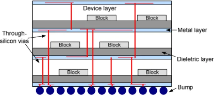
state-of-the-art 3D integration technologies, through-silicon via (TSV) is one of the most promising methods to accomplish vertical interconnects between different layers [4]. Fig. 1 illustrates a typical TSV-based 3D IC structure. By utilizing the wafer/die bonding techniques, TSVs cut across thinned silicon substrates to make inter-die connections, which results in high compatibility with the present typical CMOS processes. All external I/O signals must pass through those metal bumps located at the bottom of the 3D structure to bridge the internal logic and the external system [11]–[13].
Observation and Motivation
Compared with a typical 2D design, though a TSV-based 3D design can generally reduce the global interconnect delay, currently available TSV fabrication processes still suffer from relatively low yield as well as large TSV pitch size [14]. It is reported that in 22nm technology a TSV with 8μm pitch occupies roughly the same area as 1k SRAM cells (0.061μm2)[1], and TSV yield drops to about 80% in a 3D design with 2k TSVs [15]. Therefore, using less number of TSVs to complete a 3D design is highly desirable in terms of both yield and area cost. As a consequence, the issue of TSV minimization must be properly addressed in a design flow as stepping into the 3D IC era.
In general, 3D IC backend flows can be roughly classified into two categories. The first one is to combine TSV minimization into later design processes such as floorplanning [16] and placement [17][18], which aims at both objectives at the same time. However, the above mix-in-one problem is likely to become too complicated to be well handled. Alternatively, the authors in [19]–[21] all suggest that it is crucial to make 3D partitioning an independent stage in the backend flow as shown in Fig. 2. The suggested flow first partitions a given design into different layers and then solves the remaining problem by classical 2D techniques or their simple extensions. Hence, this methodology efficiently reduces the problem complexity while keeping the quality of results nearly at the same level [19][20]. Since the outcome of 3D partitioning mainly determines the number of required TSVs, several previous studies have been proposed to
5
tackle the problem of 3D partitioning for TSV minimization. One solution is to solve the problem using integer linear programming (ILP) [22]. However, it can only solve small-size problem since its runtime grows exponentially as problem size increases. In [23][24], each of them develops a modified FM-based [25] partitioning method to obtain the resultant layer assignment. However, all these methods only focus on minimizing the total amount of TSVs or die area, and do nothing about evenly distributing TSVs among layers. Meanwhile, the authors of 3D FPGA synthesis frameworks TPR [26] and 3D MEANDER [27] alternatively use a two-step approach – first applying the well-known partitioning algorithm hMetis [28] to divide a design into a set of layer-unaware partitions, and then associating each partition with a layer (i.e., layer assignment) – to accomplish 3D design partitioning. Though hMetis is an efficient and effective multi-way min-cut partitioning tool, it lacks for the notion of layer. In general, a typical 2D partitioning algorithm basically gives a similar weight to a cut between any two partitions, whereas those weights can vary a lot in 3D partitioning and highly depend on whether two partitions (i.e., layers) are close or far away from each other.
Indeed, 3D designs can help minimize long interconnects through the extensive use of TSVs. However, utilizing too few TSVs may limit this benefit and even increase the total wirelength, while allocating too many TSVs surely enlarges design area size [14]. Though only focusing on TSV reduction cannot guarantee decrease of wirelength after placement and routing, a TSV-minimized (also area-minimized) partitioning technique should still be incorporated as a
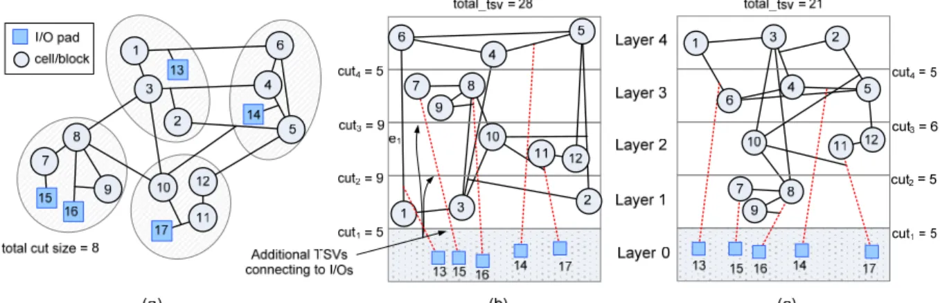
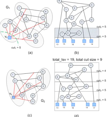
Figure 3 (a) A 4-way min-cut partitioned design, (b) the worst possible, and (c) the best possible 3D layering outcomes based on the partitioning in (a).
6
preprocessing stage in a 3D design flow, which provides a good starting point for further tradeoff between area and wirelength in the following stages.
Fig. 3 demonstrates a simple 4-layer 3D partitioning example. A given design with its 4-way min-cut partitioning result is presented in Fig. 3(a). Based on the same initial partitioning result given in Fig. 3(a), Fig. 3(b) and 3(c) respectively illustrate the worst possible and the best possible 3D layering outcomes in terms of the number of TSVs. From the observations on Fig. 3, here we would like to highlight two key ideas.
Firstly, all external I/O terminals must be located in the bottom-most layer. It implies those square vertices representing I/O pads must always be located in Layer 0. As a result, extra TSVs are required to properly relocate those I/O pads. As shown in Fig. 3(b), five additional signal paths (in dotted lines) suggest that 13 more TSVs are further required. Those extra signal paths are generally unconsidered in conventional multi-way min-cut partitioning algorithms. It also explains why there is a big difference between the total cut size (=8) in Fig. 3(a) and the number of total TSVs (=28) in Fig. 3(b).
Secondly, different layer assignments usually result in different TSV requirements even the given initial partitioning result is identical. For instance, given the partitioning result shown in Fig. 3(a), the total number of TSVs can range from 21 to 28 after examining all possible layer assignments. Nevertheless, the best layering result with the minimum number of TSVs shown in Fig. 6(d) cannot be derived from the initial partitioning outcome shown in Fig. 3(a), which is obtained from hMetis.
According to the aforementioned discussions, it should be evident that conventional multi-way min-cut partitioning algorithms virtually have no chances to perform 3D partitioning well in their original forms due to their unawareness about the fundamentals of vertical die-stacking structure. Therefore, a layer-aware partitioning algorithm specifically dedicated to 3D structures is strongly demanded for advanced 3D IC design methodologies.
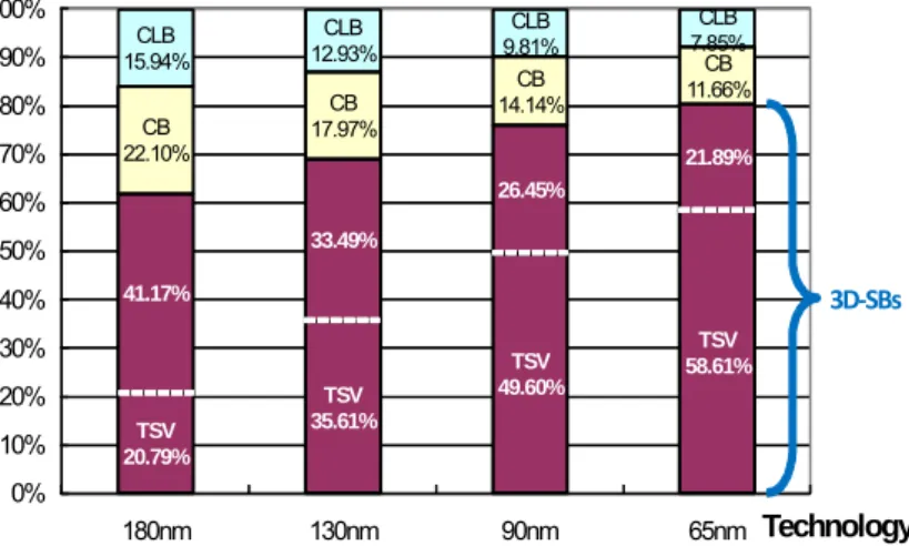
Meanwhile, according to [1][26][29], the SB has already been the most area-consuming unit compared to the other elements in 2D FPGAs for a long time. The situation is becoming even worse in 3D FPGAs because the 3D-SB is exactly where those TSVs locate. As shown in Fig. 4, as manufacturing technology keeps scaling down, the area share of the 3D-SB is getting more dominant, which is mainly because TSVs are not scaled well. Moreover, it is found that the TSV utilization is actually quite low if the 3D-SB with full vertical connectivity is in use. As depicted
TSV 20.79% TSV 35.61% TSV 49.60% TSV 58.61% 41.17% 33.49% 26.45% 21.89% CB 22.10% CB 17.97% CB 14.14% CB 11.66% CLB 15.94% CLB 12.93% CLB 9.81% CLB 7.85% 0% 10% 20% 30% 40% 50% 60% 70% 80% 90% 100% 180nm 130nm 90nm 65nm Technology 3D‐SBs
7
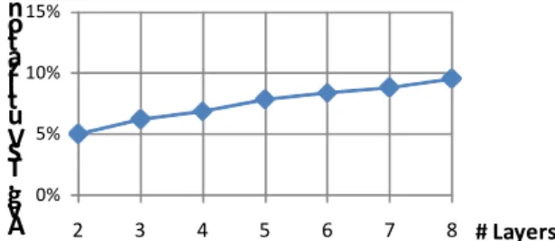
in Fig. 5, the TSV utilization is still less than 10% even in the 8-layer 3D FPGA. Therefore, there is a strong motive to optimize the 3D-SB structure and the 3D-SB deployment strategy for area saving.
3D MEANDER is another design framework for 3D FPGAs. In addition, it also studies the impact of different deployment strategies for 3D-SBs. It proposes a family of 3D FPGA architectures in which 2D-SBs and 3D-SBs are mixed up in certain regular spatial patterns. However, the number of available TSVs within a 3D-SB is assumed fixed in 3D MEANDER. That is, it does not investigate what the impact of the different number of TSVs in a 3D-SB is.
In this project, we first point out that the utilization of TSVs is actually very low in a 3D FPGA architecture with full vertical connectivity, which inspires us to discover new architectures that can achieve a better balance between area and delay. There are basically two ways for area reduction: reducing the number of TSVs in a 3D-SB, and reducing the number of 3D-SBs. In combination of above two ideas, we propose two major families of architectures and extensively evaluate numerous instances through thorough and systematic comparisons to pick out the better ones. Note that minimizing area only is one thing, but minimizing area without sacrificing delay is completely another thing.
三、 研究方法與成果
This project indicates the design issues when integrating 3D stacking technology into regular architectures. This emerging technology allows stacking multiple layers of dies and typically resolves the vertical inter-layer connection issue by TSVs. However, TSVs also occupy significant silicon estate as well as incur reliability problems. The deployment of TSVs must be very judicious in 3D designs. An iterative layer-aware partitioning algorithm, named iLap, for TSV minimization in 3D structures is proposed. On the other hand, a generic 2D FPGA architecture can evolve into a 3D one by extending its signal switching scheme from 2D to 3D by means of TSVs. However, replacing all 2D switch boxes (SBs) by 3D ones with full vertical connectivity is found both area-consuming and resource-squandering. Therefore, it is possible to greatly reduce the footprint with only minor delay increase by properly tailoring the structure and deployment strategy of 3D SB. In this project, we also perform a comprehensive architectural exploration of 3D FPGAs. Various architectural alternatives are proposed and then evaluated thoroughly to pick out the most appropriate ones with a better area/delay balance.
0% 5% 10% 15% 2 3 4 5 6 7 8 A vg . T SV u ti liz at io n # Layers
8
Layer-Aware Iterative Partitioning A. Problem formulation
A design is modeled as a hypergraph G = (V, E), where V is a set of vertices including a set of functional cells (or blocks) C and a set of I/O pads I (i.e., V = C ∪ I, C ∩ I = ); and E is a set of hyperedges. For each vertex v V, area(v) denotes the area cost of v. Each hyperedge is a subset of V, i.e., e V e E. A k-layer disjoint partition set of G with all the I/O terminals
residing in the bottom-most layer is represented as L = {L0=I, L1, L2 … Lk}, where Li is the partition assigned to the i-th layer and is a subset of C; i.e., Li C 1 i k; Li ∩ Lj = i
j, 1 i, j k; and L1 ∪ L2 ∪…∪Lk = C.
For a vertex v, layer(v) indicates which layer v actually resides in. That is, layer(v) = i, v
Li. The range pair of a hyperedge e is defined as rp(e) = (b, t) if e connects vertices from the lower b-th layer to the upper t-th layer; i.e., v e, b layer(v) t. Then the number of TSVs required to complete e can be calculated as tsv(e) = t – b. The layer junction jcti is defined as the junction between the two adjacent layers Li–1 and Li, 1 i k. The number of TSVs passing through jcti is further defined as cuti. Hence, the total number of TSVs, total_tsv, needed for a 3D partitioning solution L can be determined either by summing the required TSVs for all hyperedges ( ) or by summing TSVs passing through all junctions ( ). Consider the example shown in Fig. 3(b), rp(e1) = (1, 4) and thus tsv(e1) = 3. Similarly, the total
number of TSVs in Fig. 3(b) is total_tsv = = 5 + 9 + 9 + 5 = 28, including 15 TSVs connecting between cells, and 13 TSVs connecting cells and I/O pads. We would like to emphasize again that classical partitioning algorithms usually have no idea about the I/O pad connection constraint and always underestimate the real TSV demand even excluding those TSVs for connecting cells and I/O pads (8 vs. 15 in the case shown in Fig. 3(a) and 3(b)) due to their layer-unawareness. Those are the major reasons why the classical min-cut-based partitioning solutions are generally not well optimized in 3D cases (shown later).
In this paper, we model the 3D partitioning problem as a layer-aware multi-way partitioning problem. Given a target 3D structure consisting of k layers stacking vertically, a design G, and the I/O pad constraint, our proposed algorithm partitions G into k sub-designs and each sub-design is explicitly associated with a vertical layer so that the total number of TSVs is minimized. That is, given G = (V = C ∪ I, E) with layer(v) = 0 v I, our algorithm directly finds the mapping, 1
layer(v) k v C, such that total_tsv is minimizeds.
B. Proposed algorithm
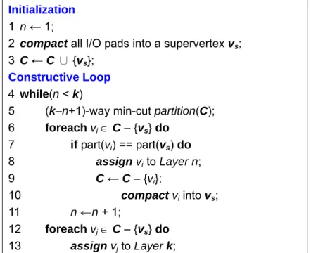
Here we propose our iterative partitioning framework that gradually constructs the solution from the bottom-most layer all the way to the topmost one. Consider that all I/O pads must reside in L0 by definition and then the number of TSVs through jct1 (i.e., cut1,) is always fixed to |I| no
matter how other cells (or L1~Lk) get partitioned eventually. As a result, if we define G1 by
compacting all the I/O pads into a supervertex vs and keeping all the connected hyperedges unchanged as shown in Fig. 6(a), it is evident that jct1 and cut1 should still remain unchanged in G1. Next, an arbitrary conventional k-way area-balanced min-cut partitioning algorithm is applied
on G1 to get k partitions, where area(vs) is set to zero to avoid disturbing area balancing during partitioning. Among those k disjoint partitions, exactly one partition ps can contain vs, which
9
further suggests that the cells residing in ps should be located as close to the I/O pads as possible for cut minimization and thus should be assigned to L1. For example, the four dashed circles in
Fig. 6(a) indicate the 4-way area-balanced min-cut partitioning result, and hence L1 is ultimately set to {7, 8, 9} as Fig. 6(b) depicts.
Similarly, once the elements of L1 are determined, cut2 is therefore fixed. The next task then
becomes how to decide which vertices should reside in L2. Again, since L0 and L1 are fixed at this
point, jct2 and cut2 are both fixed no matter how other remaining cells (or L2~Lk) get partitioned
later. As one can easily discover that the situation here is very similar to that of identifying L1
previously. Hence, if we further derive G2 from G1 by compacting L1 into vs and apply (k–1)-way min-cut partitioning on G2, L2 can then be identified in the same fashion (as shown in Fig. 6(c)).
That is, at each iteration our proposed algorithm always derives Gn+1 from Gn by further compacting Ln into vs, then applies (k–n)-way area-balanced min-cut partitioning to get Ln+1. This iterative process is not terminated until Lk–1 is identified. Fig. 6(d) illustrates the final result generated by the proposed algorithm, and the total TSV count is merely 19, which is smaller than those in Fig. 3(b) and 3(c) (28 and 21, respectively).
The proposed framework possesses following four unique features:
It invokes multi-way min-cut partitioning at every iteration. The major reason is to find the set of cells closest to the previously identified junctions, which potentially minimizes the TSVs of the current junction. To better mimic the final solution, min-cut partitioning helps distribute TSVs more evenly among all layers and hence potentially results in a more stable outcome.
Figure 6. (a) Compact I/O pads into vs then apply 4-way partitioning, (b) assign {7, 8 ,9} to L1, (c) compact L1 into vs then apply 3-way partitioning, and (d) show the final layering result
10
Once a junction (and thus a cut) is fixed at some iteration, it is never altered at the following iterations. This ensures that good decisions made previously are never overthrown later. At each iteration, only one partition is accepted and decisions for other partitions are
actually discarded. Later, the updated graph topology is reexamined and better decisions are thus dynamically reacquired at the following iterations. For instance, L2 = {1, 3, 10} in Fig.
6(d) is not identical to any partition shown in Fig. 6(a). As a consequence, applying any one of conventional multi-way min-cut partitioning algorithms just once cannot get this kind of result.
From the traditional partitioning perspective, the result in Fig. 6(d) has a larger total cut size than the result given in Fig. 3(a) (9 vs. 8). However, we already show that the former one is actually a better 3D partitioning solution. Hence, it is obvious that the total cut size, which is layer-unaware, is apparently not an appropriate metric in 3D partitioning. Again, this is another evidence that classical multi-way min-cut partitioning algorithms can hardly compete with the proposed iterative framework.
In this work, we adopt the well-known hMetis as the internal partitioning engine since it is one of the best partitioning engines we can find today. However, our proposed framework can obviously co-work with any multi-way min-cut partitioning engines. It implies that a better engine (if any) may be adopted for better 3D partitioning results in the future.
The pseudo code of the complete algorithm is given in Fig. 7. All I/O pads are first compacted into a supervertex vs during initialization. Each iteration starts with (k–n+1)-way min-cut partitioning. Once partitioning is done, the vertices residing in the partition where vs is present are assigned to the current layer, i.e., Layer n. The number n always increases by one at every iteration end. At the final iteration, where n = k–1, the elements of Layer k–1 are identified after 2-way partitioning. Finally, the remaining cells are then automatically assigned to the topmost Layer k and the algorithm ends. That is, exact k–1 invocations of multi-way min-cut partitioning are required for getting one k-layer 3D partitioning result here.
Initialization
1 n ← 1;
2 compact all I/O pads into a supervertex vs; 3 C ← C ∪ {vs};
Constructive Loop
4 while(n < k)
5 (k–n+1)-way min-cut partition(C); 6 foreach vi C – {vs} do 7 if part(vi) == part(vs) do 8 assign vi to Layer n; 9 C ← C – {vi}; 10 compact vi into vs; 11 n ←n + 1; 12 foreach vj C – {vs} do 13 assign vj to Layer k;
11
C. Experiments
1. Benchmarks and Experiment Setup
iLap has been implemented in C++/Linux environment. We demonstrate the effectiveness of iLap through a series of comparisons with three hMetis-based methods: 1) hMetis: partitions are further layered according to their original sequential tags (i.e., in random order basically); 2) EX-hMetis: partitions are best layered through exhaustively examining all possible layer permutations; 3) EV-matrix: partitions are layered by the method described in [26]. Note that the three hMetis-based methods all start with the same set of partitions and thus the variances among their final results solely come from different layer assignments. We evaluate the performance of iLap and other three methods over a set of 14 test cases, consisting of 10 cases from the MCNC benchmark set [30], three large cases (cfft, aqua, and video) from Altera [31], and one in-house 128-point FFT design (fft128). They are intended to mimic complicated system designs integrating a large number of functional blocks. The number of blocks ranges from 1,047 to 53,491. Since the test cases selected in our experiments are all far larger than those used in [22], comparisons between iLap and the ILP-based approach proposed in [22] are therefore omitted in this paper. We perform ten experiment runs on every test case with different random seeds and take the average as the final result.
2. Results and Analyses
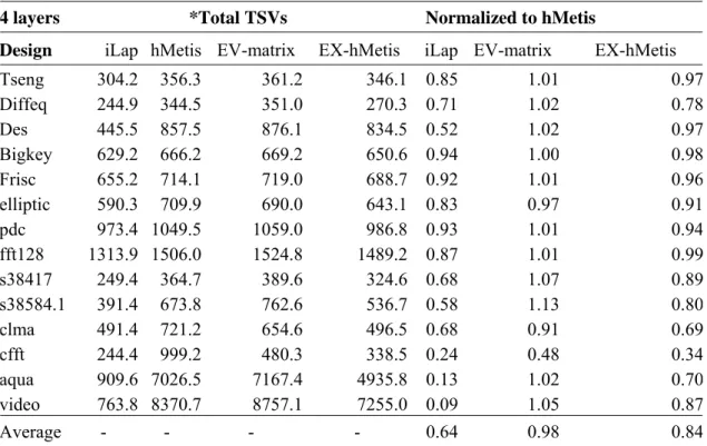
A set of experiments are conducted with various number of layers ranging from two to ten. Table I reports the TSV demands as the number of layers is set to 4. It seems EV-matrix just performs equally well as plain hMetis. Meanwhile, given a set of 4 partitions generated by hMetis, EX-hMetis always picks the one with the lowest TSV count out of 4! = 24 different layer permutations and consequently EX-hMetis on average attains 16% TSV reduction as compared with hMetis. Nevertheless, iLap can reduce TSV count by 36% and 24% on average as compared to hMetis and EX-hMetis, respectively. Moreover, for the largest three test cases (cfft, aqua, and video), iLap even outperforms hMetis by more than 75%. Though hMetis is an excellent multi-way min-cut partitioning algorithm, unfortunately it fails to be a good 3D partitioner due to its layer-unawareness. Even EX-hMetis, with exhaustive layer permutations, still cannot
0 1000 2000 3000 4000 5000 2 3 4 5 6 7 8 9 10 Layers (a) TSV count iLap hMetis EV-matrix EX-hMetis 0.5 0.7 0.9 1.1 1.3 1.5 1.7 2 3 4 5 6 7 8 9 10 Layers (b) Normalized TSV count iLap hMetis EV-matrix EX-hMetis
12
defeat iLap. Therefore, it concludes that a dedicated layer-aware 3D partitioning algorithm, like iLap, should be regarded as one of the essential components while constructing a sophisticated 3D IC design environment.
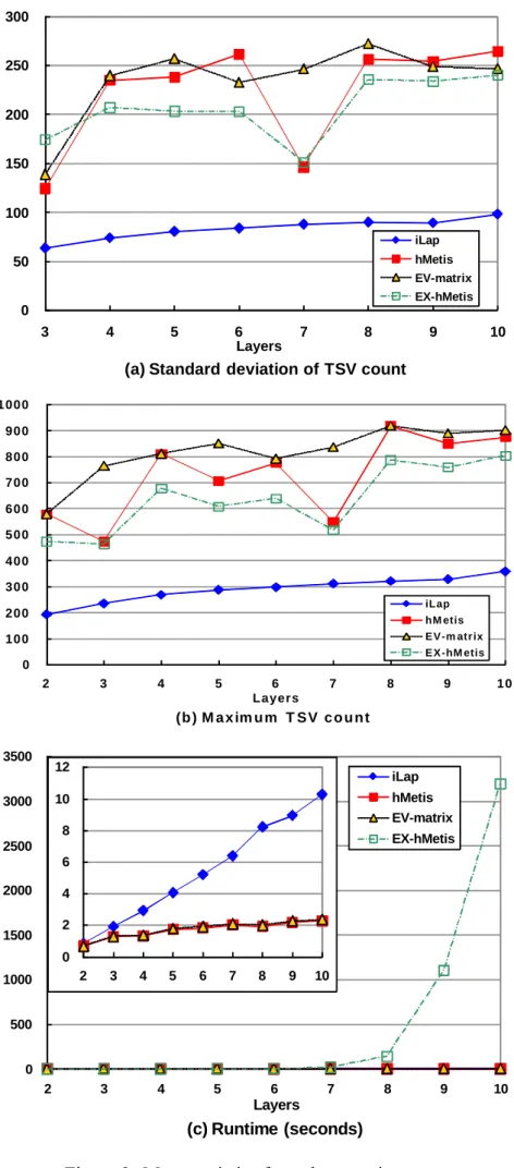
Next, Fig. 8(a) depicts the average TSV count over 14 test cases as a function of the number of layers; and three points are worth pointing out. Firstly, the more layers a design gets partitioned into, the more TSVs it generally requires. Secondly, iLap is the all-time winner from 2 layers to 10 layers among four methods. Thirdly, unlike the other three methods, the number of TSVs required by iLap raises very smoothly as the number of layers increases. Taking hMetis as the baseline, Fig. 8(b) reveals the average ratios of TSV count over the number of layers; and two points are worth mentioning here. Firstly, iLap constantly and steadily outperforms hMetis by about 35% in TSV count regardless of the number of layers. Secondly, EX-hMetis always outperforms hMetis, as expected. Meanwhile, Fig. 9(a) presents the average standard deviations of TSV count over a different number of layers. Through constructing its outcome layer by layer, iLap can better balance the TSV count among junctions. From Fig. 9(a), it is evident that the standard deviation of TSV count associated with iLap is far better than those of the other three. As previously mentioned, a TSV occupies significant silicon estate so that high standard deviation of TSV count potentially worsens area imbalance among individual layers and even lowers the yield of a design. Fig. 9(b) reports the average maximum TSV count at some junction of a design over a different number of layers; and iLap always possesses the lowest values regardless of the number of layers. In other words, a lower TSV count implies a smaller total area (including TSV area) after partitioning, and a smaller standard deviation of TSV count results in a more area-balanced partitioning outcome. The above two facts suggest that iLap tends to generate a smaller overall footprint of a 3D chip implementation. From another perspective, for some 3D logic
TABLEI. TOTAL NUMBER OF TSVS WITH K =4
4 layers *Total TSVs Normalized to hMetis
Design iLap hMetis EV-matrix EX-hMetis iLap EV-matrix EX-hMetis
Tseng 304.2 356.3 361.2 346.1 0.85 1.01 0.97 Diffeq 244.9 344.5 351.0 270.3 0.71 1.02 0.78 Des 445.5 857.5 876.1 834.5 0.52 1.02 0.97 Bigkey 629.2 666.2 669.2 650.6 0.94 1.00 0.98 Frisc 655.2 714.1 719.0 688.7 0.92 1.01 0.96 elliptic 590.3 709.9 690.0 643.1 0.83 0.97 0.91 pdc 973.4 1049.5 1059.0 986.8 0.93 1.01 0.94 fft128 1313.9 1506.0 1524.8 1489.2 0.87 1.01 0.99 s38417 249.4 364.7 389.6 324.6 0.68 1.07 0.89 s38584.1 391.4 673.8 762.6 536.7 0.58 1.13 0.80 clma 491.4 721.2 654.6 496.5 0.68 0.91 0.69 cfft 244.4 999.2 480.3 338.5 0.24 0.48 0.34 aqua 909.6 7026.5 7167.4 4935.8 0.13 1.02 0.70 video 763.8 8370.7 8757.1 7255.0 0.09 1.05 0.87 Average - - - - 0.64 0.98 0.84
13
structures, like 3D FPGAs, the number of pre-fabricated inter-layer TSVs is fixed. Hence a design mapping attempt is considered a failure as long as the required TSVs exceed the available ones only at one junction; and a high maximum TSV count definitely increases such chances. Lower maximum TSV count is considered a big plus especially in design flows for 3D regular logic structures such as 3D FPGAs.
Regarding the runtime efficiency issue, Fig. 9(c) gives the average runtime of 14 test cases in second over a different number of layers. It is evident that both hMetis and EV-matrix are very time-efficient. The runtime required by iLap grows linearly as the number of layers increases. It is mainly because the number of invocations for multi-way partitioning inside iLap also grows linearly as the number of layers increases. However, given the tremendous performance in TSV minimization, the time complexity of iLap should be acceptable. For example, it only takes about fifty seconds for iLap to partition the largest test case video into ten layers. As for EX-hMetis, since it has to check all possible layer permutations to find out the best one, the required runtime is thus exponential to the number of layers. Even if EX-hMetis can be further improved (e.g., by pruning) so that not all permutations need to be examined, the improvement is limited to runtime efficiency only, while other TSV-related performance would still remain the same.
14 0 50 100 150 200 250 300 3 4 5 6 7 8 9 10 Layers
(a) Standard deviation of TSV count iLap hMetis EV-matrix EX-hMetis 0 100 200 300 400 500 600 700 800 900 1000 2 3 4 5 6 7 8 9 10 Layers (b ) M a x im u m T S V c o u n t iLap hM etis E V -m atr ix E X -hM etis 0 500 1000 1500 2000 2500 3000 3500 2 3 4 5 6 7 8 9 10 Layers (c) Runtime (seconds) iLap hMetis EV-matrix EX-hMetis 0 2 4 6 8 10 12 2 3 4 5 6 7 8 9 10
15
Architectural Exploration of 3D FPGAs towards a Better Balance between Area and Delay A. Architectures and synthesis framework for 3D FPGAs
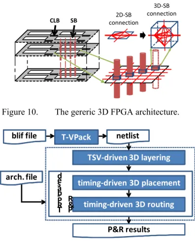
A classic 2D FPGA is composed of logic elements (configurable logic blocks, CLBs) and routing resources (switch boxes, SBs; connection boxes, CBs). The basic unit is called a tile, which consists of a CLB, an SB, and associated CBs. As shown in Fig.10, the generic 3D FGPA architecture in this work is similar to the one used in TPR and 3D MEANDER, which basically stacks multiple identical 2D FPGA layers and then extends the structure of 2D-SB to provide inter-layer connectivity. Fs is set to 3 in a 2D-SB and 5 in a 3D-SB, where Fs is the maximum allowable fan-outs of a channel in an SB.
The reference synthesis flow used in this work is shown in Fig. 11. A given design (in blif format) is first packed into a netlist file composed of CLBs by T-VPack, which is a part of the 2D FPGA synthesis framework VPR [32][33]. The netlist file is then fed into a 3D FPGA synthesizer, which includes three steps: initial layering, timing-driven 3D placement and 3D routing. The initial layering partitions the netlist into different layers with the objective of TSV minimization [34]. The 3D placement and routing processes, which are adapted from TPR, are then conducted on the layered netlist. The framework also takes an input file, setting the architectural parameters of the target 3D FPGA, and generates the placement and routing results in the end.
B. Evaluation environment 1. Architectural Settings
The basic architectural settings are shown in TABLE II. Most of the parameters are set according to existing commercial FPGAs, well-known FPGA synthesizers, and related
CLB SB connection2D‐SB
3D‐SB connection
Figure 10. The gereric 3D FPGA architecture.
timing‐driven 3D routing TR P ‐b as e d P & R TSV‐driven 3D layering P&R results timing‐driven 3D placement netlist T‐VPack blif file arch. file
16
research works [26][27][29], [35]–[38]. The number of LUTs (lookup tables) in an CLB (N) is set to 2 instead of 1 in the previous works [26][29], which is considered more realistic. The channel widths in the X-Y directions are both set to 32; the multi-segment routing structure is adopted: the possible wire lengths are L1, L2, L4 and L8; and the numbers of channels are 12, 12, 4 and 4, respectively. In the vertical direction (Z), only L1 is available to maximize the routability. Finally, I/O pads are located only around the bottom-most layer.
2. Benchmark Set
There are 24 test cases in our benchmark set – 14 are from MCNC and the other 10 larger ones are from IWLS2005, ITC99 and Altera [30][31]. The basic information for a
TABLEII. THE ARCHITECTURAL SETTINGS
Architectural Parameters Value
CLB
(Altera Stratix IV)
# of LUTs in a CLB (N) 2 # of inputs of a CLB (I) 8 # of inputs of a LUT (K) 6 SB
(Xilinx Spartan) Connection type Subset
Channel width
(Xilinx) Both WX and WY 32
# of wire segments X-Y direction (L1, L2, L4, L8) (12, 12, 4, 4) Z direction L1 only -
Delay model L1Z : L1X-Y 1 : 10
TSV Pitch 10 um
Process Technology 65 nm
TABLEIII. THE BENCHMARK INFORMATION (PARTIAL) Design # CLBs # Nets # I/Os
s38584.11 3224 5419 342 clma1 4192 6869 144 mem_ctrl_0mv_b2 7344 10865 265 usb_funct_0mv_b2 7440 11372 234 tv80_0abc_ch2 8809 12987 46 b203 9844 15557 55 b213 10016 15713 55 aes_core2 10400 16706 386 oc_des_perf_opt_opt_abc_resyn4 10641 17150 185 systemcaes_0abc_ch2 13480 19634 388 b223 14585 23114 55 b173 15390 24986 135
17
partial set of test cases is shown in TABLE III; the numbers of CLBs and nets are derived from T-VPack with the parameters (N, I, K) = (2, 8, 6), which is specified in TABLE II.
In our evaluation environment, the X-Y dimension (D) of a 3D FPGA architecture varies according to the number of layers (L) and the overall capacity of CLBs (C), as given in (1):
(1)
During every evaluation run, the capacity of CLBs (C) is dynamically adjusted to ensure that the value is around 80%.
3. Baseline Architecture (BSL)
In the baseline architecture, every SB is a 3D-SB; and every 3D-SB is with full vertical connectivity, which means there are 32 TSVs (identical to the number of channels in the X-Y direction) within a 3D-SB. In the BSL, though the vertical routability is maximized (which is best to delay), the utilization of TSVs is extremely low (< 10%) as indicated in Fig. 5. This fact also suggests there is still a big room for further architecture improvements. Hereafter in this paper, the BSL would serve as a baseline for comparisons with the proposed architectures in the next two sections.
C. Proposed sparse architectures
Basically there are two ways to reduce the area occupied by 3D-SBs in a 3D FPGA. The first one is to decrease the number of TSVs in a 3D-SB. Such kind of 3D-SBs are called partially
(a)
(b)
(c)
fully connected 3D‐SB partially connected 3D‐SB 2D‐SB18
connected 3D-SBs. The other one, also used in 3D MEANDER, is to reduce the number of 3D-SBs in a 3D FPGA. That is, some SBs become 3D ones, and others are still 2D ones. The internally-spare (IS) architectures are those utilizing the former method, while the externally-sparse (ES) ones are those utilizing the latter method. Different configurations of SBs, also referred as patterns in this paper, are shown in Fig. 12. In the BSL, as shown in Fig. 12(a), all SBs are fully connected 3D-SBs. An IS architecture adopts the same type of partially connected 3D-SBs for all SBs instead, as in Fig. 12(b). In an ES architecture as shown in Fig. 12(c), fully connected 3D-SBs are partially distributed in a regular fashion. Note that the patterns are set identical for all layers in all proposed architectures. In addition to IS and ES architectures, the sparse architecture (SP), which is a hybrid of the above two, is proposed to further reduce the area. More details and evaluations are available in the following sub-sections.
1. Internally-Sparse Architecture (IS)
IS# represents an instance of the IS architecture, where the postfix # specifies the number of TSVs available in a 3D-SB. For example, every 3D-SB in IS16 has only 16 TSVs inside, while IS32 is actually equivalent to the BSL. As mentioned in Section III, the multi-segment routing structure is adopted and there are four different wire lengths with different amount of channels in the X-Y direction. In the BSL, it makes no differences since each X-Y channel has its own vertical connection. However, in an IS
89.99% 79.98% 69.98% 59.97% 49.96% 39.95% 90.89% 81.78% 72.67% 63.57% 54.46% 45.35% 0% 10% 20% 30% 40% 50% 60% 70% 80% 90% 100%
IS28 IS24 IS20 IS16 IS12 IS8 N o rm a liz e d a re a SB Tile
Figure 13. The normalized area of different IS architectures.
100% 103% 106% 109% 112% 115% 118% 2 3 4 5 6 7 8
A
vg
. n
o
rm
a
li
ze
d
d
e
la
y
# Layers IS8 IS12 IS16 IS2019
architecture, some of TSVs in a 3D-SB are removed. Be precisely, the vertical connections (TSVs) are taken out from each type of X-Y channels proportionally whenever possible. For example, the numbers of channels with vertical (Z) connectivity for ( L1, L2, L4, L8) are (9, 9, 3, 3) in IS24, while the remaining 8 channels merely provide 2D (X-Y) connectivity.
Fig. 13 reports the area of different IS architectures, in which all values are normalized to that of the BSL. It shows that both the sizes of an SB and a tile basically decrease linearly as the number of TSVs in a 3D-SB decreases. However, though reducing the number of TSVs in an 3D-SB can save area, it is very likely to harm delay at the same time. To realize what the exact impact on delay is, the benchmark circuits are mapped onto different IS architectures and the BSL through the reference synthesis framework. Fig. 14 illustrates the delay of different IS architectures, in which every value represents the average of normalized-to-the-BSL delay over the entire benchmark set. Since the curves of IS28, IS24, and IS20 are almost overlapped therefore only the one of IS20 is depicted. Note that some test cases fail to be mapped onto IS12 due to insufficient vertical routing channels. Most of the test cases fail in IS8; one even succeeds, the delay increases significantly. Finally, since IS20 achieves about 30% overall area reduction only with a delay penalty less than 1.5% as compared to the BSL, it should be the one with a better area/delay balance among all IS architectures.
2. Externally-Sparse Architecture (ES)
An ES architecture replaces a part of fully connected 3D-SBs with 2D-SBs for area saving. There are various ways, or patterns, for mixing 2D-SBs and 3D-SBs. The pattern used in the ES architecture is oblique stripes, which is the same as the one used in 3D MEANDER. ES# represents an instance of the ES architecture, where the postfix # specifies the maximum distance between two adjacent 3D-SBs in either X or Y direction. Therefore, ES1 is actually equivalent to the BSL, and ES2 is the one shown in Fig. 15(a). Different from the vertical or horizontal stripes patterns, it is guaranteed that each 3D-SB in the oblique stripes pattern can reach some other 3D-SBs within a fixed distance in any directions, which surely provides much better routability. From the perspective of a 2D-SB, the shaded region covers the area where a 2D-SB can access vertical links in the
(a) (b)
fully connected 3D‐SB
2D‐SB
Figure 15. The ES architecture with
20
shortest distance as shown in Fig. 15(a). However, with the same shaded region, only two 3D-SBs can be reached for a 2D-SB in an architecture with vertical stripes patterns, as shown in Fig. 15(b). The analyses and conclusions are also similar also from the perspective of a 3D-SB.
Fig. 16 reports the area of different ES architectures. As the distance increases, the area reduction is significant at first and then becomes flat gradually. The curve appears like a harmonic sequence. Fig. 17 illustrates the delay of different ES architectures. As the distance increases, the delay is increased badly. As a result, ES2, ES3 and ES4 are all regarded as good instances since they can achieve around 35%~55% area reduction only with a delay penalty less than 5%. Moreover, if the delay penalty is constrained below 3%, ES2 becomes the best choice because it achieves an area reduction of 35% with a delay penalty less than 1.5%.
3. Sparse Architecture (SP)
For IS and ES architectures, we try to reduce the area with just a single strategy – either purely reducing the number of TSVs in each 3D-SB or purely reducing the number of 3D-SBs. Here we present the sparse architecture, which takes above two strategies simultaneously. SP(#1, #2) is used to name an specific instance of this hybrid architecture,
which is the combination of IS#1 and ES#2. This notation can be generalized to represent
IS and ES architectures as well. For example, SP(32, 1) is equivalent to the BSL, SP(16, 1) implies IS16, and SP(32, 2) is actually ES2. Meanwhile, the TSV density of an
100% 103% 106% 109% 112% 115% 118% 121% 2 3 4 5 6 7 8
A
vg
. n
o
rm
a
li
ze
d
d
e
la
y
# Layers ES9 ES8 ES7 ES6 ES5 ES4 ES3 ES2Figure 17. The average normalized dealy of different ES architectures.
60.01% 46.68% 40.04% 36.08% 33.40% 31.53% 30.16% 29.09% 63.60% 51.47% 45.43% 41.83% 39.39% 37.69% 36.43% 35.46% 0% 10% 20% 30% 40% 50% 60% 70% 80% 90% 100%
ES2 ES3 ES4 ES5 ES6 ES7 ES8 ES9
N o rm al iz e d a re a SB Tile
21
architecture is defined as the average number of TSVs in a tile, and can be calculated through (2).
TSV density = IS# / ES# (2)
As mentioned, ES4=SP(32, 4) with TSV density of 8 is still regarded as a good instance. Note that, the lower the TSV density is, the worse the delay is likely to be. Hence, only those SP architectures with TSV density no less than 8 are selected for evaluation. Fig. 18 shows the area of selected SP architectures. As expected, the lower the TSV density is, the smaller the area is. Fig. 19 reports the delay of same selected SP architectures, and conforms that the lower the TSV density is, the worse the delay is. Finally, SP(28, 2), SP(24, 2), and SP(20, 2), are our recommended SP architectures under the constraint that the delay penalty cannot exceed 3%.
D. Proposed sunny egg architecture
Though SP(20, 2) has already achieved an area reduction of 50% with minor delay loss, there is still room for improvement. Fig. 20 shows the average TSV distribution in a 6-layer BSL over 6 test cases. The results suggest that the TSV demand is much bigger in the central region than
55.00% 49.99% 44.98% 43.34% 40.00% 39.97% 59.04% 54.49% 49.93% 48.43% 45.39% 45.37% 0% 10% 20% 30% 40% 50% 60% 70% 80% 90% 100% (28,2) (24,2) (20,2) (28,3) (24,3) (16,2) N o rm al iz e d a re a SB Tile TSV density: 14 12 10 9.3 8 8
Figure 18. The normalized area of different SP architectures.
100.0% 100.5% 101.0% 101.5% 102.0% 102.5% 103.0% 103.5% 104.0% 104.5% 105.0% 2 3 4 5 6 7 8 A vg . n o rm al iz e d d e la y # Layers (16,2) 8 (24,3) 8 (28,3) 9.3 (20,2) 10 (24,2) 12 (28,2) 14 TSV density:
22
that in the peripheral zone; and thus inspire us to further propose the sunny egg (SE) architecture. The sunny egg architecture divides a horizontal plane into two regions – center (egg yolk) and periphery (egg white). Two regions are implemented using different SP architectures – the TSV density in the center is set larger than that in the periphery. SE(ISC#, ESC#, R, ISP#, ESP#) indicates a specific SE architecture, where SP(ISC# and ESC#)/SP(ISP# and ESP#) is for the center/periphery respectively, and R is the ratio between the dimension of the center and D (defined in Section III.B). For example, SE(32, 2, 0.5, 16, 4) specifies an SE architecture: 1) in the central/peripheral region, the number of TSVs in a 3D-SB is 32/16 and the distance between two 3D-SBs in the X/Y directions is 2/4; and 2) the ratio between the dimension of center and D
(a)
(b)
(c)
11‐12 9‐10 7‐8 5‐6 ≦ 4Figure 20. The average TSV utilization in a 6-layer BSL. Between: (a) Layer 2 and 3, (b) Layer 3 and 4, and (c) Layer 4 and 5.
100.0% 101.5% 103.0% 104.5% 106.0% 2 3 4 5 6 7 8
A
vg
. n
o
rm
a
li
ze
d
d
e
la
y
# Layers unevenly (center) evenly (center) unevenly (periphery) evenly (periphery)Figure 21. The average normalized dealy with different TSV distributions.
100.0% 101.5% 103.0% 104.5% 106.0% 107.5% 2 3 4 5 6 7 8
A
vg
. n
o
rm
al
iz
e
d
d
e
la
y
# Layers R=0.3 R=0.4 R=0.5 R=0.6 R=0.723
is 0.5.
A total of 20 different SE architectures are evaluated in this study. They are generated in the following way: 2 SP instances with higher TSV densities (SP(32, 2), SP(16, 1)) for the center, 2 SP instances with lower TSV densities (SP(16, 4), SP(8, 2)) for the periphery, and R ranges from 0.3 to 0.7. TABLE III just lists 8 of them due to page limitation. Meanwhile, given the same TSV density, SP(16, 1) distributes TSVs more evenly than SP(32, 2) in the center. Similarly, SP(8, 2) distributes TSVs more evenly than SP(16, 4) in the periphery.
Fig. 21 demonstrates how the different TSV distributions can impact the delay. First, it suggests that it is better to distribute TSVs unevenly in the center, i.e., SP(32, 2) is preferred. Second, the delay is slightly better if TSVs are evenly distributed in the periphery, i.e., SP(8, 2) is preferred.
The ratio R also does matter. As mentioned previously, the TSV density in the center is always larger than that in the periphery. Hence, the bigger the ratio R is, the larger the footprint is. Meanwhile, as shown in Fig. 22, the delay gets better as R increases due to richer routing resources. Consequently, as usual, it is still a trade-off between delay and area. Again, to keep the delay penalty less than 3% compared to the BSL, R must be set to higher than 0.6. As a result, the best choice here should be SE(32, 2, 0.6, 8, 2).
All the architectures mentioned above are compared and evaluated thoroughly. The one with the smallest 3D-SBs area while keeping the performance (i.e., the delay penalty is less than 3%
TABLEIV . SEARCHITECURES UNDER EVALUATION (PARTIAL) ISC# ESC# R ISP# ESP# 32 2 0.3 16 4 32 2 0.3 8 2 16 1 0.3 16 4 16 1 0.3 8 2 32 2 0.7 16 4 32 2 0.7 8 2 16 1 0.7 16 4 16 1 0.7 8 2 100.00% 85.76% 64.28% 60.17% 100.00% 87.52% 68.70% 65.10% 0% 10% 20% 30% 40% 50% 60% 70% 80% 90% 100% IS20=(20,1) ES2=(32,2) (20,2) (32,2,0.6,8,2) N o rm a liz e d a re a (t o I S2 0 ) SB Tile
24
compared to BSL) are chosen as the representation of each architectural style. As shown in Fig. 23, the normalized (to IS20 instead of BSL in the previous evaluations) area consumptions of IS20, ES2, SP(20, 2) and SE(32, 2, 0.6, 8, 2) are depicted. The average normalized delay (to BSL) is shown in Fig. 24. The hybrid architectures, which utilize both the techniques of IS and ES, can save more than 35% area of SBs compared to IS20. Especially, the difference of delay penalty between SE(32, 2, 0.6, 8, 2) and IS20 is less than 2%. Therefore, the hybrid architectures SP(20, 2) and SE(32, 2, 0.6, 8, 2) are the most recommended.
四、 結論
In this project, we present an iterative layer-aware partitioning algorithm iLap targeting TSV minimization for 3D structures. It utilizes a multi-way min-cut partitioning engine inside its iterative framework to gradually construct the final solution layer by layer in the bottom-up fashion. The experimental results clearly demonstrate that iLap is capable of reducing total TSV count by about 35% compared to layer-unaware hMetis, experiencing a smoother TSV increase as the number of layers raises, distributing TSVs more evenly among different vertical layers, preventing any layer junction from having a burst number of TSVs, and only requires an acceptable runtime. Consequently, compared to the prior art, we believe iLap can generate a better TSV-minimized solution, which serves as a good starting point for further tradeoff between wirelength and number of TSVs in upcoming state-of-the-art 3D IC/FPGA design flows.
Moreover, we show that the utilization of TSVs is actually very low in the baseline 3D FPGA architecture where the fully connected 3D-SBs are fully distributed. Therefore the area of 3D FPGAs can be further reduced while the performance is still guaranteed. There are two simple approaches to reduce the area of 3D-SBs. The internal-sparse architecture (IS) is to reduce the number of TSVs in each single 3D-SB and the external-sparse 3D-SBs architecture (ES) is to reduce the number of 3D-SBs. The hybrid methods, including sparse architecture (SP) and sunny egg (SE), are also proposed to further minimize the area of 3D FPGAs by using the techniques of IS and ES at the same time. Those architectures are explored thoroughly and evaluated objectively. After comparing all these architectures, two generic 3D FPGA architectures are suggested, that is, the SP architecture (20, 2) and SE architecture (32, 2, 0.6, 8, 2), which save the most area with acceptable delay penalty. SP(20, 2) reduces 55% (to BSL) and 35% (to IS20) of SB area; SE(32, 2, 0.6, 8, 2) reduces 58% (to BSL) and 39% (to IS20) of SB area. Both of them are with (less than) 3% increase delay.
100.00% 100.75% 101.50% 102.25% 103.00% 2 3 4 5 6 7 8 A vg . n o rm a li ze d d e la y # Layers (20, 2) (32,2,0.6,8,2) ES2 IS20
25
五、 參考文獻
[1] International Technology Roadmap for Semiconductor. Semiconductor Industry Association, 2009.
[2] K. Banerjee, S. J. Souri, P. Kapur, and K. C. Saraswat, “3-D ICs: a novel chip design for improving deep submicron interconnect performance and systems-on-chip integration,” Proc. IEEE, vol. 89, no. 5, pp. 602–633, 2001.
[3] A. W. Topol, D. C. La Tulipe, L. Shi, D. J. Frank, K. Bernstein, S. E. Steen, A. Kumar, G. U. Singco, A. M. Young, K. W. Guarini and M. Ieong, “Three-dimensional integrated circuits,” IBM J. of Research and Development, vol. 50, no. 4/5, pp. 491–506, Jul./Sep. 2006.
[4] G. Philip, B. Christopher, and P. Ramm, Handbook of 3D integration. Wiley-VCH, 2008. [5] S. Das, A. P. Chandrakasan, and R. Reif, “Calibration of rent's rule models for
three-dimensional integrated circuits,” IEEE Trans. Very Large Scale Integration Systems, vol. 12, no. 4, pp. 359–366, Apr. 2004.
[6] M. Lin, A. El Gamal, Y.-C. Lu, and S. Wong, “Performance benefits of monolithically stacked 3-D FPGA,” IEEE Trans. Computer-Aided Design Integrated Circuits and Systems, vol.26, no.2, pp.216–229, Feb. 2007.
[7] C. Dong, D. Chen, S. Haruehanroengra, and W. Wang, “3-D nFPGA: A Reconfigurable Architecture for 3-D CMOS/Nanomaterial Hybrid Digital Circuits,” IEEE Trans. Circuit and System I: Regular Papers, vol. 54, no. 11, pp. 2489–2501, Nov. 2007.
[8] R. R. Tummala and V. K. Madisetti, “System on chip or system on package?” IEEE Design & Test of Computers, vol. 16, no. 2, , pp. 48–56, Apr.–Jun., 1999.
[9] P. H. Shiu and K. S. Lim, “Multi-layer floorplanning for reliable system-on-package,” Proc. 2004 Int’l Symp. Circuits and System, May 2004, pp. 23–26.
[10] K. L. Tai, “System-in-package (SIP): challenges and opportunities,” Proc. Asia and South Pacific Design Automation Conf., 2000, pp. 191–196.
[11] W. R. Davis et al., “Demystifying 3D ICs: the pros and cons of going vertical,” IEEE Design and Test of Computers, vol. 22, no. 6, pp. 498–510, Nov.–Dec., 2005.
[12] I. Loi, S. Mitra, T. H. Lee, S. Fujita, and L. Benini, “A low-overhead fault tolerance scheme for TSV-based 3D network on chip links,” Proc. Int’l Conf. Computer-Aided Design, 2008, pp. 598–602.
[13] C. Ferri, S. Reda, and R. I. Bahar, “Parametric yield management for 3D ICs: models and strategies for improvement,” J. Emerging Technologies in Computing Systems, vol. 4, no. 4, Article ID 19, Oct. 2008.
26
[14] M. Pathak, Y.-J. Lee, T. Moon, and S. K. Lim, “Through-silicon via management during 3D physical design: when to add and how many?” Proc. Int’l Conf. on Computed-Aided Design, pp. 387–394, 2010.
[15] A.-C. Hsieh, T. Hwang, M.-T. Chang, M.-H. Tsai, C.-M. Tseng and H.-C. Li, “TSV redundancy: architecture and design issues in 3D IC,” Proc. Design, Automation & Test in Europe Conf. & Exibit., pp. 166–171, 2010.
[16] Z. Li, X. Hong, Q. Zhou, S. Zeng, J. Bian, W. Yu, H. H. Yang, V. Pitchumani, and C.-K. Cheng, “Efficient thermal via planning approach and its application in 3-D floorplanning,” IEEE Trans. on Computer-Aided Design of Integrated Circuits and Systems, vol. 26, no. 4, pp. 645–658, Apr. 2007.
[17] B. Goplen and S. Sapatnekar, “Placement of 3D ICs with thermal and interlayer via considerations,” Proc. Design Automation Conf., pp. 626–631, 2007.
[18] J. Cong and G. Luo, “A multilevel analytical placement for 3D ICs,” Proc. Asia and South Pacific Design Automation Conf., pp. 361–366, 2009.
[19] Z. Li, X. Hong, Q. Zhou, Y. Cai, J. Bian, H. H. Yang, V. Pitchumani, and C.-K. Cheng, “Hierarchical 3-D floorplanning algorithm for wirelenth optimization,” IEEE Trans. on Computer-Aided Design of Integrated Circuits and Systems, vol. 53, no. 12, pp. 2637–2646, Dec. 2006.
[20] V. F. Pavlidis and E. G. Friedman, “Interconnect-based design methodology for three-dimensional integrated circuits,” Proc. IEEE, vol. 97, no. 1, pp. 123–140, Jan. 2009. [21] C. Chiang and S. Sinha, “The road to 3D EDA tool deadiness,” Proc. Asia and South Pacific
Design Automation Conf., pp. 429–436, 2009.
[22] I. H.-R. Jiang, “Generic integer linear programming formulation for 3D IC partitioning,” 22nd IEEE Int’l SOC Conf., pp. 321–324, 2009.
[23] D. H. Kim, K. Athikulwongse, and S. K. Lim, “A study of through-silicon-via impact on the 3D stacked IC layout,” Proc. Int’l Conf. on Computer-Aided Design, pp. 674–680, 2009. [24] Y. C. Hu, Y. L. Chung, and M. C. Chi, “A multilevel multilayer partitioning algorithm for
three dimensional integrated circuits,” Proc. Int’l Symp. on Quality Electronic Design, pp. 483–487, 2010.
[25] C. M. Fiduccia and R. M. Mattheyses, “A linear time heuristic for improving network partitions,” Proc. Design Automation Conf., pp.175–181, 1982.
[26] C. Ababei, H. Mogal, and K. Bazargan, “Three-dimensional place and route for FPGAs,” IEEE Trans. on Computer-Aided Design of Integrated Circuits and Systems, vol. 25, no. 6, pp. 1132–1140, Jun. 2006.
27
[27] K. Siozios, A. Bartzas, and D. Soudirs, “Architecture-level exploration of alternative interconnection schemes targeting to 3D FPGAs: a software-supported methodology,” Int’l J. of Reconfigurable Computing, vol. 2008, Article ID 764942, 2008.
[28] G. Karypis, R. Aggarwal, V. Kumar, and S. Shekhar, “Multilevel hypergraph partitioning: applications in VLSI domain,” IEEE Trans. on VLSI Systems, vol. 7, no. 1, pp. 69–79, Mar. 1999.
[29] TPR: three-dimensional placement and route for FPGAs. [Online]. Available: http://www.ece.umn.edu/users/kia/mount/Download/
[30] S. Yang, “Logic synthesis and optimization benchmarks user guide,” Technical Report 1991-IWLS-UG-Saeyang, Microelectronics Center of North Carolina, 1991.
[31] http://www.eecs.berkeley.edu/~alanmi/benchmarks/altera/old/altera12_blif_baf.zip..
[32] A. Marquardt, V. Bets, and J. Rose, “Timing-driven placement for FPGAs,” Proc. Int’l Symp. Field Programmable Gate Arrays, Feb. 2000, pp. 203–213.
[33] VPR: versatile packing, placement and routing for FPGAs. [Online]. Available: http://www.eecg.toronto.edu/~vaughn/vpr/vpr.html
[34] Y.-S. Huang, Y.-H. Liu, and J.-D. Huang, “Iterative 3D partitioning for through-silicon via minimization,” Proc. 16th Workshop on Synthesis and System Integration of Mixed Information Technologies, Oct. 2010.
[35] K. Siozios, V. F. Pavlidis, and D. Soudris, “A software-supported methodology for exploring interconnection architectures targeting 3-D FPGAs.” Proc. Design, Automation & Test in Europe Conf. and Exhibition, 2009, pp. 172–177.
[36] Altera. [Online]. Available: http://www.altera.com/ [37] Xilinx. [Online]. Available: http://www.xilinx.com/
[38] C. S. Tan, R. J. Gutmann, and L. R. Reif, Editors, Wafer level 3-D ICs process technology, MA: Springer, 2008.
六、 成果自評
我們於計劃第二年的這段期間(99 年 8 月 1 日至 100 年 7 月 31 日),在學術論文發表 方面,在今年度我們發表了以下國際會議論文:
1. Ya-Shih Huang and Juinn-Dar Huang, “Throughput-Driven Hierarchical Placement for Two-Dimensional Regular Multicycle Communication Architecture," Asia Symposium on Quality Electronic Design, pp. 134–139, Aug. 2010.
2. Ya-Shih Huang, Yang-Hsiang Liu, and Juinn-Dar Huang, “Iterative 3D Partitioning for Through-Silicon Via Minimization," Proc. of the 16th Workshop on Synthesis and System Integration of Mixed Information Technologies, pp. 154–159, Oct. 2010.
28
3. Chia-I Chen, Bau-Cheng Lee, Juinn-Dar Huang, “Architectural Exploration of 3D FPGAs towards a Better Balance between Area and Delay," Proc. of Design, Automation & Test in Europe Conference and Exhibition, pp. 587–590, Mar. 2011. (Best Paper Candidate)
4. Juinn-Dar Huang, Yi-Hang Chen, and Wan-Hsien Lin, “Performance-Optimal Behavioral Synthesis with Degenerable Compound Functional Units,” Proc. of IEEE International Symposium on VLSI Design, Automation, and Test, pp. 337–340, Apr. 2011.
5. Ya-Shih Huang, Yang-Hsiang Liu and Juinn-Dar Huang, “ Layer-Aware Design Partitioning for Vertical Interconnect Minimization," Proc. of IEEE Computer Society Annual Symposium on VLSI, pp. 144–149, Jul. 2011. (Best Paper Award)
還有以下國內會議論文:
1. Ya-Shih Huang, Yang-Hsiang Liu, and Juinn-Dar Huang, “Layer-Aware Partitioning for Through-Silicon Via Minimization in 3D ICs," Proc. of the 21st VLSI Design/CAD Symposium, Aug. 2010.
在專利方面,通過以下國內外專利:
1. 黃俊達,林步青,李耿維,周景揚,“精細頻寬調控的仲裁器及其仲裁方法" 中華民 國專利案號 I332615,2010 年 11 月 1 日。
2. Juinn-Dar Huang and Chia-I Chen, “Dynamical sequentially-controlled low-power multiplexer device,” US 7881241 B2, Feb. 2011.
3. 黃俊達,陳嘉怡,“低功率動態序向控制多工器" 中華民國專利案號 I342670,2011 年5 月 21 日。
並有以下專利正在申請中:
1. 黃俊達、呂智宏、林步青、周景揚,“應用於查找表式 FPGA 的壓縮樹延遲最佳化”。 2. 黃俊達、王毓翔、林步青、周景揚,“可參數化管線式快速傳利葉轉換硬體產生器”。 3. 黃俊達、呂智宏、林步青、周景揚,Delay optimal compressor tree synthesis for LUT-based
FPGAs .
和我們當初在計劃提案中的預計的目標相比較,我們自評今年度計劃的完成度相當不 錯,其中更有一篇論文獲得 ISVLSI 2011 會議之最佳論文獎(Best paper award),一篇論文於 VLSI-DAT 2011 會議中獲最佳論文候選(Best paper candidate),在學術論文發表及專利方面 皆有不錯的表現,。
29
可供推廣之研發成果資料表
□ 可申請專利 ▓ 可技術移轉 日期:100 年 10 月 31 日國科會補助計畫
計畫名稱: 針對三維規則型邏輯結構之架構探索及穩健合成系統開發 計畫主持人:黃俊達 副教授 國立交通大學電子系 計畫編號:NSC99-2220-E-009-037- 學門領域:微電學門技術/創作名稱
適用於三維電路之層級感知矽穿孔最小化設計分割法(Layer-Aware Design Partitioning for Vertical Interconnect Minimization)
發明人/創作人
黃雅詩、劉揚翔、黃俊達技術說明
中文: 我們針對三維積體電路發展一套能夠最佳化矽穿孔數目之迭代式 層級感知分割演算法。此演算法應用多路最小切割法將電路以迭代 的方式逐層分配至適合的層級中,使其更能考慮全域的分佈狀況, 而達到更好的效果。同時也在不違反輸入及輸出腳位必須在晶片底 層的限制下,進而改善三維的積體電路。 英文:We propose an iterative layer-aware partitioning algorithm, named iLap, for TSV minimization in 3D structures. iLap iteratively applies multi-way min-cut partitioning to gradually divide a given design layer by layer in the bottom-up fashion. Meanwhile, iLap also properly fulfills a specific I/O pad constraint incurred by 3D structures to further improve its outcome.
可利用之產業
及
可開發之產品
1. Electronic Design Automation (EDA) (EDA 產業) 2. Integrated Circuit Design (IC 設計產業)