0040-6090/02/$ - see front matter䊚 2002 Elsevier Science B.V. All rights reserved. PII: S 0 0 4 0 - 6 0 9 0 Ž 0 2 . 0 0 9 3 9 - 2
Electrical properties of metal–ferroelectric–insulator–semiconductor using
sol–gel derived SrBi Ta O film and ultra-thin Si N buffer layer
2 2 9 3 4Chia-Hsing Huang , Tseung-Yuen Tseng *, Chao-Hsin Chien , Ming-Jui Yang , Ching-Chich Leu ,
a a, b b bTing-Chang Chang , Po-Tsun Liu , Tiao-Yuan Huang
b,cb bInstitute of Electronics, National Chiao Tung University, Hsinchu 30050, Taiwan, ROC
a
National Nano Device Laboratory, Hsinchu 30050, Taiwan, ROC
b
Department of Physics, National Sun Yat-sen University, Kaohsiung 804, Taiwan, ROC
c
Abstract
The electrical properties of the metal–ferroelectric–insulator–silicon memories with stacked gate configuration of Pty
SrBi Ta O2 2 9 (SBT)ySi N yp-Si (1 0 0) were investigated. In an attempt to operate at low voltage with sufficient large memory3 4
window, various ultra-thin Si N buffer layers in thickness of 3.5, 2, and 0.9 nm were employed. From the results of3 4 C–V
measurements, the memory window can be as large as 0.8 V at the bias amplitude of 5 V for the sample with 0.9 nm Si Nx y
buffer layer. Well-crystallized perovskite structures have been further confirmed by the spectra of X-ray diffraction measurements. The leakage current, which plays a very important role in the data retention, of PtySBT(245 nm)ySi N (0.9 nm)yp-Si (1 0 0)3 4
can be as low as 2.5=10y8 Aycm at 200 kVycm. Excellent fatigue-free performance with up to 102 10 readywrite cycles and
good retention time of )2 h have been obtained. Optimization and scaling of SBT thin films are believed to be effective in pursuing extremely low voltage operation, high-density and liable 1T nonvolatile ferroelectric random access memories.
䊚 2002 Elsevier Science B.V. All rights reserved.
Keywords: SrBi Ta O ; Metal–ferroelectric–insulator–semiconductor; SiN; Data retention; Fatigue; Memory window2 2 9
1. Introduction
The metal–ferroelectric–insulator–semiconductor
(MFIS) has been attracting much attention as a prom-ising structure for the high-density and high-speed FET-type nonvolatile memories, which are usually denoted as FeMFET w1x. FeMFETs have several advantages over the ferroelectric random access memories with 1T1C cell structure, such as smaller cell size, simple process integration and, especially, nondestructive readout char-acteristic. The introduction of additional insulator in the system cannot only prevent the reaction and inter-diffusion between the ferroelectric film and silicon substrate, but also further improve the retention proper-ties w2,3x. However, the presence of such additional insulator will distribute some voltage drop from the applied voltage, the magnitude of which depends on the capacitance ratio of the ferroelectric film and the
insu-*Corresponding author. Tel.: 5712121; fax: q886-3-5724361.
E-mail address: [email protected](T.-Y. Tseng).
lator. This extra voltage drop will, therefore, result in the reduction of the electric field in the ferroelectric film and cause unfavorable non-saturated polarization
behavior. Using ultra-thin Si N insulator cannot only3 4
prevent inter-diffusion between ferroelectric film and Si substrate but also alleviate the electric field reduction issue in the MFIS structure. In this work, we employ the PtySrBi Ta O2 2 9 (SBT)ySi N yp-Si (1 0 0) system to3 4 study the impacts of Si N buffer layers on the electrical3 4 properties of the MFIS structures by varying the thick-ness of the buffer layer and ferroelectric annealing temperature.
2. Experimental
P-type (1 0 0) Si wafer was used as the starting
substrate. Prior to the deposition of thin films, the Si wafer was cleaned using a Radio Corporation America method, followed by a chemical etching with diluted
HF solution. The 2- and 3.5 nm-thick Si N films were3 4
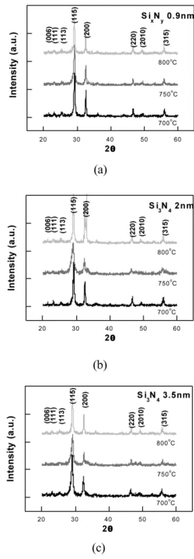
Fig. 1. XRD patterns of the SBT films deposited on (a) 0.9 nm Si Nx yySi;(b) 2 nm and (c) 3.5 nm Si N ySi substrates. The annealing3 4
temperatures vary from 700 to 800 8C.
the low-pressure chemical vapor deposition, while the ultra-thin Si N film of ;0.9 nm was carried out by thex y
surface nitridation in NH atmosphere at 800 8C. The3
thicknesses of the insulators were determined using the n&k analyzer. Subsequently, the SBT films of 245 nm were deposited on the Si N3 4ySi and Si N ySi substratesx y by the metal organic decomposition technique. After
spin-coating of precursor solution on the SiNySi
sub-strate, the film was dried at 150 8C and then pyrolysized at 400 8C for 10 min in air. This process sequence was repeated 5 times until the desire thickness was obtained. Thereafter, the films were subjected to a 1-min rapid thermal annealing under an oxygen atmosphere at vari-ous temperatures for crystallization. The surface mor-phologies and thicknesses of the SBT films were
examined by scanning electron microscopy(SEM). The
film crystallinity was investigated by X-ray diffraction (XRD). In order to inspect the electrical properties of SBT thin films, 100 nm top electrode Pt was deposited by the sputtering using the shadow mask with 150, 250 and 350 mm diameters. After that, a 5 min 400 8C N2 anneal was employed in order to form a good interface between Pt and SBT. Finally, a 500 nm back electrode Al was deposited using the thermal coater. The
capaci-tance–voltage(C–V), current density–electric filed (J–
E), fatigue, and retention characteristics were measured with a HP4284A LCR meter at a frequency of 100 kHz, HP4156A, and HP8110 function generator.
3. Results and discussion
The XRD patterns of the SBT films deposited on 2 and 3.5 nm Si N3 4ySi and 0.9 nm Si N ySi substrate arex y shown in Fig. 1. The crystallization temperatures are 700, 750 and 800 8C, respectively. Clearly, strong peaks
indicative of perovskite phase, such as (1 1 5) and
(2 0 0) preferential orientations, have been observed. Unlike the results of the previous work w4x, temperature only has a minor effect on the crystallinity of the SBT films. More importantly, even at the temperature of 700 8C, excellent crystallinity can be obtained. It seems that the incorporation of the buffer layer is helpful for crystallization in the lower temperature range. However, the thickness of the buffer layer has insignificant effect in improving the crystallinity. Fig. 2 shows the SEM
images of the SBT films deposited on Si Nx y(0.9 nm)y
Si crystallized at different temperatures. The grain sizes become slightly larger with increasing annealing tem-perature and well-crystallized structures have been
observed. Fig. 3 shows the capacitance–voltage (C–V)
characteristics of the MFIS capacitors, in which SBT was annealed at 750 8C, where the measuring frequency was 100 kHz. The voltage was swept from q5 to y5
V and then reversed. The clockwise traces in the C–V
hysteresis curves are clearly observed. It means that
split of C–V curves in two opposite polarity is due to
the polarization of the SBT films, not caused by injection charge effect w3,5x. The hysteresis window widths for the MFIS capacitors with 0.9-, 2- and 3.5 nm-thick SiN buffer layer are 0.8, 0.5 and 0.6 V, respectively. Surface nitridation is more effective than thin SiN layers in improving the memory window. The rapid changes of
Fig. 2. SEM images of SBT films deposited on Si Nx y(0.9 nm)ySi with(a) 700 8C; (b) 750 8C; (c) 800 8C annealing.
Fig. 3. Normalized capacitance–voltage (C–V) characteristics of MFIS structures, in which SBT was annealed at 750 8C, measured at 100 kHz with a voltage sweep from q5 to y5 V and reverse.
the capacitances in the depletion region indicate good interface properties have been achieved at the interface of the substrate and SiN buffer layers w3x. To evaluate
the annealing temperature and insulator thickness effects
on leakage mechanism of the PtySBTyinsulatorySi
capacitors, current density vs. electric field (J–E) char-acteristics are measured in accordance with the annealing temperature and insulator thickness, as shown in Fig. 4. Fig. 4a shows the leakage current densities of the MFIS capacitors annealed at various temperatures. The
mag-nitudes of current density are 1.8=10y8, 2.5=10y8,
and 8.5=10y8 Aycm at 200 kVycm for the samples2
annealed at 700, 750 and 800 8C, respectively. Leakage current increases with increasing temperature. This is due to the larger grain size in higher temperature, which
has been observed in the SEM results (Fig. 2). Larger
grain size is likely to lead to rougher interface between
SBT and Si N . Locally enhanced electric field couldx y
exist and, therefore, induce larger leakage current w2x. Fig. 4b shows the leakage current densities of the MFIS capacitors with different thicknesses of buffer layers.
The magnitudes of current density are 2.5=10y8,
7.7=10y8, and 3.6=10y8 Aycm at 200 kVycm for2
the samples with 0.9-, 2-, 3.5 nm-thick SiN, respectively. Surface nitridation obviously suppresses the lowest leak-age current even though its thickness is thinnest. It is speculated that surface nitridation forms denser films and smoother interfaces, than nitride reactive deposition.
Thus, the MFIS capacitor with 0.9 nm Si N bufferx y
layer can depict the lowest current density. While the leakage current densities of the capacitors with SiN layers are found to increase as the thickness of buffer layer decreases. This is consistent with the conventional effect of insulator thickness on the electrical properties of the system. The retention performance is shown in Fig. 5. The retention of a MFIS capacitor was measured by applying the writing pulses of "5 V in height and 2 ms in duration, and then reading capacitance at a voltage of 0.5 V every 20 min for 2 h. It is found that the retention is strongly correlated to the magnitude of leakage current density through the stacked gate insula-tor. The capacitor with a 0.9 nm-thick Si N buffer layer,x y
Fig. 4.(a) Annealing temperature effects on leakage mechanism of the PtySBTy0.9 nm Si N ySi capacitors;x y (b) insulator thickness effects on leakage mechanism of the PtySBTyinsulatorySi capacitors.
Fig. 6. Fatigue properties of the MFIS with various thickness insu-lators as a function of switching cycles of "5 V in height and 1 MHz in frequency.
Fig. 5. Retention performances of the MFIS capacitors.
which has the lowest leakage current density, also exhibits the best retention performance. The fatigue properties of the MFIS capacitors with various insulators were also measured. Fig. 6 shows both accumulation and depletion capacitance readings at 0.5 V as a function of switching cycles. The amplitude of the bipolar pulse train is "5 V in height and the frequency is 1 MHz. It can be clearly seen that all the capacitors demonstrate
excellent nearly fatigue-free performance up to 1010
cycles as exhibited in SBT thin films.
4. Conclusion
Using SiN as buffer layer can lower the crystallization temperature of the SBT thin films down to 700 8C with only 1 min annealing. It has been proven with the strong peaks indicative of perovskite phases in the X-ray patterns. The memory window of 0.8 V can be achieved at voltage sweep "5 V. The leakage current of the
capacitor with the configuration of PtySBT (245 nm)y
Si N3 4 (0.9 nm)yp-Si (1 0 0) can be as low as
2.5=10y8Aycm at 200 kVycm. It was also found that2
the fabricated MFIS capacitors exhibit long retention
performances and fatigue-free characteristics up to 1010
switching cycles.
Acknowledgments
The authors gratefully appreciate the financial support from the National Science Council of Republic of China under Project No. NSC-90-2215-E009-100. Thanks are
also due to the Semiconductor Research Center (SRC)
in National Chiao Tung University and the National
Nano Device Laboratory(NDL) of the R.O.C. NSC for
References
w1x J.-P. Han, T.P. Ma, Appl. Phys. Lett. 72(1998) 1185. w2x M. Noda, Y. Mstsumudo, H. Sugiyama, M. Okuyama, Jpn. J.
Appl. Phys. 38(1999) 2275–2280.
w3x K.-J. Choi, W.-C. Shin, J.-H. Yang, S.-G. Yoon, Appl. Phys. Lett. 75(1999) 722.
w4x W.-J. Lee, C.-H. Shin, C.-R. Cho, J.-S. Lyu, B.-W. Kim, Jpn. J. Appl. Phys. 38(1999) 2039–2043.
w5x T. Yamaguhi, M. Koyama, A. Takashima, S.-I. Takagi, Jpn. J. Appl. Phys. 39(2000) 2058–2062.