國 立 交 通 大 學
電控工程研究所
碩 士 論 文
應用於車用電子之電力線通訊收發器設計
Transceiver Design of Power Line Communication
for Automotive Electronics
研 究 生:鄭鈞藝
指導教授:蘇朝琴 陳鴻祺 教授
Transceiver Design of Power Line Communication for
Automotive Electronics
研 究 生:鄭鈞藝 Student : Chun-Yi Cheng
指導教授:蘇朝琴 教授 Advisor : Chau-Chin Su
陳鴻祺 教授 Hung-Chi Chen
國 立 交 通 大 學
電控工程研究所
碩士論文
A ThesisSubmitted to Institute of Electrical Control Engineering College of Electrical Engineering and Computer Science
National Chiao Tung University in partial Fulfillment of the Requirements
for the Degree of Master
in
Electrical Control Engineering
November 2010
Hsinchu, Taiwan, Republic of China
研究生 : 鄭鈞藝 指導教授 : 蘇朝琴 教授
陳鴻祺 教授
國立交通大學電控工程研究所
摘 要
近年來車用電子(automotive electronics)越來越受到重視,許多研究或產品多著重在 多媒體以及娛樂等的發展。因此,在汽車自動化的程度越來越高以及車內電子控制單元 也越來越多的情況下,在接線上也就越來越複雜,所以我們將焦點轉移到車內元件彼此 之間的資料傳輸。我們將電力線通信(power line communication)與車用電子結合在一 起,每個裝置都會需要一條線連到車上的電源,這個是沒辦法省略的,所以要是我們可 以同時在電源線上面供給電源又同時傳輸資料的話,便可使接線簡單化,既可降低複雜 度又能省成本。我們利用電源線當作傳輸訊號的通道,為了達到抗拒外界雜訊的干擾, 我們利用了直接序列展頻技術(direct sequence spread spectrum)來對資料做編碼,使得訊 噪比可以提升。我們也設計了一個應用於此技術的收發器,在資料與時脈恢復器上,將 相位選擇與應用在 DSSS 的傳統架構結合在一起。我們也設計了一個具有封包的 32 位 元的串列解串器,使得我們只需要一條電源線就可達到資料的傳輸。整體系統包含了傳 送端、接收端、耦合電路、電源線以及後端的控制電路,控制電路負責的是接收到資料 後產生訊號來控制 LED、馬達以及降壓電路的亮度、閃爍頻率、閃爍的亮度、轉速以及 輸出電壓。我們利用 FPGA 來實現 TX、RX 以及後端的控制電路,然後將 PowerMOS、 LED、馬達、降壓電路、開關等利用印刷電路板來整合,展示了資料傳輸及控制元件的 能力,證明了此電路設計是能夠被實現出來且非常實際的,以及將電力線通信用在車用 電子上的想法是可行的。關鍵字: 電力線通信(power line communication)、車用電子(automotive electronics)、 直接序列展頻技術(direct sequence spread spectrum)
Automotive Electronics
Student: Chun-Yi Cheng Advisor: Chau-Chin Su
Hung-Chi Chen
Institute of Electrical Control Engineering
National Chiao Tung University
Abstract
In recent years, the importance and diversity of the automotive electronics has attracted more and more attention. Most of the applications are centered on the multimedia or entertainment. Here we focus on the data communication between the electronic devices on the car. We apply the power line communication to the automotive electronics. DC 12V power line of the car is used as the transmission media. We use direct sequence spread spectrum (DSSS) modulation to the data signal in order to resist the noise interference. We design a clock and data recovery (CDR) circuit which combines the phase picking for clock recovery and byte synchronization for data recovery. We realize a transceiver with DSSS and a 32-bit SERDES. The whole system includes a transmitter, a receiver, a coupling circuit and a control circuit. A delta-sigma digital pulse width modulator (ΔΣ-DPWM) driver is implemented for the power driving. The control circuit adjusts PWM for on-time duty and frequency control of the LEDs, controls the rotation speed of the motors and the output voltage of DC-DC converter. We use FPGA to realize the transmitter and receiver which includes the control circuit. We put PowerMOS, LED, motor, buck converter, switches and coupling circuits on the printed circuit boards. Finally, we demonstrate the data transmission and controlling of the devices. We prove the idea of power line communication for automotive electronics is feasible.
Keyword: power line communication, automotive electronics, direct sequence spread spectrum (DSSS)
誌 謝
首先要感謝的是我的指導教授 蘇朝琴老師,總是告訴我們要不斷的去思考,當問 題發生時不要去逃避,表面上看到的東西不一定就是真相,要仔細地去思考背後的一 切。做研究最重要的就是要培養我們的思考能力以及解決問題的能力,模擬只是輔助, 最重要的是自己的想法。不管是在學習上或是生活中,在老師的教導下,都使我獲益良 多。 此外感謝實驗室的所有學長、同學、學弟妹的幫忙與支持。謝謝丸子學長在我一 開始很灰心無助的時候開導了我,適時的點醒了我,告訴了我做研究最重要的事情,讓 我能重新振作起來。謝謝盈杰學長的鼓勵以及協助。多虧了有你的帶領,實驗室的任何 大小事都能完善的解決。謝謝仁乾學長對於 PLL 方面給了我許多的指導以及建議,也 很謝謝你能一直關心我們這些學弟。謝謝庭佑學長對於研究上面的協助,以及很辛苦的 維護實驗室的工作站及硬體設備,使我們能擁有穩定的模擬環境。謝謝洲銘、家齊學長 陪伴了我們快兩年的時間,在研究上一起討論,在生活上一起分享。很懷念晚上一起在 實驗室的日子。謝謝于昇學長在學校陪伴了我們兩年多的日子,但我們還是室友所以生 活上還是不會分開的。在未來還是能一起討論學術,一起去看表演,一起練吉他,一起 看曼聯輸給切爾西吧!謝謝土豆的一起努力,想當初也是因為我人太好才會想跟你一 組,沒想到在課業上也都跟你同一組。想到那時候我們辛苦的做研究以及量測,深怕會 做不出來的時候,到現在能夠跟你一起口試一起畢業,真的是太感動了,以後也要一起 去打球吃飯跟大潤發。也很謝謝海豹、修銘、群育、博祥,在這兩年多以來大家一起討 論功課一起做研究,雖然彼此之間做的東西是不一樣的,但都能互相給意見,在生活上 也增添了許多快樂。謝謝澤勝、璟伊、弘宇、順煜、昶志、馬克、阿 MON、小紅豆、 嘉哲學弟妹們的陪伴,在枯燥的研究生涯裡增添了許多的歡樂色彩。希望大家都能夠研 究順利以及找到自己想做的事。 最後則是要感謝我的家人,爸爸、媽媽以及妹妹。每次回到家後都能夠吃大餐然 後很放鬆的度過週末。雖然我知道你們總是會在那邊擔心什麼,但我還是很感謝你們的 關愛,畢竟家人的支持是使我能成長茁壯最大的力量。 鄭鈞藝 2010/11/09Tables of Content
Abstract in Chinese ... i
Abstract in English ... ii
Thanks ... iii
Tables of Content ... iv
List of Figures ... vi
List of Tables ...viii
Chapter 1 Introduction ... 1
1.1 Motivation ... 1
1.2 Features ... 2
1.3 Organization ... 3
Chapter 2 Background Studies ... 4
2.1 Basic Serial Link ... 4
2.2 Architecture of CDR ... 9
2.3 Direct Sequence Spread Spectrum ... 16
Chapter 3 Behavioral Simulation of the Proposed CDR ... 22
3.1 The Proposed CDR ... 22
3.2 The Block Diagram of Proposed CDR ... 23
3.3 Behavioral Simulation ... 30
3.4 Transceiver Simulation ... 34
Chapter 4 Circuit Implementation of the Transceiver ... 36
4.1 Transmitter ... 36
4.2 Receiver ... 38
4.3 Circuit Simulation of the Transceiver ... 43
Chapter 5 Realization of the System on FPGA and PCB ... 46
5.2 SERDES and Backend Control Circuit ... 49
5.3 Coupling Circuit with Power Line... 51
5.4 Integration of the System ... 52
Chapter 6 Conclusion ... 59
List of Figures
Fig. 1-1: A generalized model of a power line communication for automotive ... 2
Fig. 2-1: A generalized model of a serial link... 5
Fig. 2-2: (a) Cycle-to-cycle jitter, (b) variable cycles. ... 5
Fig. 2-3: Components of total jitter ... 6
Fig. 2-4: Jitter transfer mask ... 7
Fig. 2-5: Jitter tolerance mask ... 8
Fig. 2-6: Concept of a CDR circuit... 9
Fig. 2-7: A general function block of PLL-based type CDR [8] ... 9
Fig. 2-8: Linear PD proposed by Hogge ... 10
Fig. 2-9: A PLL-based CDR with linear PD [8] ... 10
Fig. 2-10: Bang-bang PD proposed by Alexander ... 11
Fig. 2-11: A PLL-based CDR with binary PD [10] ... 11
Fig. 2-12: A block diagram of a blind oversampling CDR [11] ... 12
Fig. 2-13: An example of phase decision ... 13
Fig. 2-14: An example of oversampling CDR [12] ... 13
Fig. 2-15: A clock interpolation CDR proposed by Ruiyuan Zhang [13] ... 14
Fig. 2-16: A data-deskew CDR proposed by Hung-Wen Lu [14] ... 15
Fig. 2-17: Power spectral density of spread spectrum signal [15]... 16
Fig. 2-18: DSSS system and modulation process [16] ... 17
Fig. 2-19: Code Synchronization [18] ... 18
Fig. 2-20: Serial search with correlator [19]... 19
Fig. 2-21: Parallel search with matched filter [19] ... 20
Fig. 2-22: Delay-locked loop [20] ... 20
Fig. 2-23: Tau-dither loop [20] ... 21
Fig. 3-1: The proposed CDR ... 23
Fig. 3-2: Accumulation and absolution results ... 24
Fig. 3-3: Correlator ... 25
Fig. 3-4: Simulation of correlator ... 26
Fig. 3-5: Phase shift FSM ... 26
Fig. 3-6: Phase shift FSM ... 27
Fig. 3-7: Types of confidence counter ... 27
Fig. 3-8: Confidence counter ... 28
Fig. 3-9: Phase control FSM ... 29
Fig. 3-10: Simulation of phase control FSM ... 29
Fig. 3-11: Phase rotation scheme ... 29
Fig. 3-14: Chips delay test ... 31
Fig. 3-15: Random jitter ... 31
Fig. 3-16: Deterministic jitter ... 32
Fig. 3-17: Simulation of RJ and DJ ... 32
Fig. 3-18: -1000ppm (clock of the data) ... 33
Fig. 3-19: +1000ppm (clock of the data) ... 33
Fig. 3-20: +1000ppm with DJ and RJ ... 34
Fig. 3-21: Transceiver system ... 34
Fig. 3-22: Transmitter ... 35
Fig. 3-23: Receiver ... 35
Fig. 4-1: Barker code ... 36
Fig. 4-2: Serializer ... 37
Fig. 4-3: Control signal for serializer ... 37
Fig. 4-4: Preamble and counter... 38
Fig. 4-5: Accumulator ... 38
Fig. 4-6: Absolute value circuit ... 39
Fig. 4-7: Confidence counter ... 40
Fig. 4-8: Phase control FSM ... 40
Fig. 4-9: Johnson counter ... 40
Fig. 4-10: Delay circuit for Ph+ phase ... 41
Fig. 4-11: Delay circuit for Php phase ... 41
Fig. 4-12: State diagram of sequence detector ... 41
Fig. 4-13: Simulation of the sequence detector ... 42
Fig. 4-14: Timing control circuit ... 42
Fig. 4-15: Deserializer ... 43
Fig. 4-16: Simulation of the transmitter ... 43
Fig. 4-17: Simulation of the receiver ... 44
Fig. 4-18: Simulation of the frequency error ... 44
Fig. 5-1: Transceiver with backend control circuit ... 46
Fig. 5-2: Test for CDR ... 47
Fig. 5-3: Test of data recovery ... 48
Fig. 5-4: Test of detection of preamble ... 48
Fig. 5-5: Test of SERDES and backend control circuit ... 49
Fig. 5-6: Power line added ... 49
Fig. 5-7: On-time 50% and PWM 50% ... 50
Fig. 5-8: On-time 25% and PWM 75% ... 50
Fig. 5-9: On-time 75% and PWM 25% ... 50
Fig. 5-10: Coupling circuit with power line ... 51
Fig. 5-12: On-time 50% and PWM 50% ... 52
Fig. 5-13: System of the application ... 52
Fig. 5-14: LED, motor, and three pairs of switches ... 53
Fig. 5-15: Buck converter, LDO, switches for transmitter and buck converter ... 53
Fig. 5-16: Results from buck converter ... 54
Fig. 5-17: Results from LED and motor ... 54
Fig. 5-18: Environment of the final test ... 55
Fig. 5-19: Sub-blocks of the final test ... 55
Fig. 5-20 Output voltage of the buck converter... 56
Fig. 5-21: Load and line regulation at output voltage 3V ... 56
Fig. 5-22: Load and line regulation at output voltage 9V ... 57
Fig. 5-23: On-time and dimming control of LED ... 57
Fig. 5-24: Rotation speed of motor ... 58
List of Tables
Table 2.1 The conversion between RMS and Peak-to-Peak of the random jitter ... 7Table 2.2 Look-up table of the control function ... 58
Chapter 1
Introduction
1.1 Motivation
As the car technology advanced rapidly, more and more electronic devices are applied on
the car, such as LED lighting, electric sunroof, electric windows, etc. are simple ones. Multimedia center, GPS navigator, ABS system, air conditioning thermostat, etc. are complex
ones. The cost of electronics in a regular car is about 15% to 25%. For a luxury one or RV, it can be over 50%, therefore, the automotive electronics is becoming increasingly popular and
important.
Observing from the automotive electronics these days, the devices on the cars have independent communication agreement, such as CAN (Control Area Network), LIN (Local
communication bus between control centers. Different agreements are used for different local control or different cars. As the device increases, the number of wires increases. The
complexity of wiring and routing becomes more and more difficult. In order to achieve the control of devices and decrease the complexity of wiring and routing, we take advantage of
the existing power line on the car to achieve the data communication.
Power line communication becomes attractive for transmission of power and data with no extra wiring [2,3,4]. The research in power line communication has been a long time. At the
beginning, they are used for measurement of loading and automation on the high voltage. Now the communication network on the medium voltage and low voltage is demanding and
popular.
But the difficulty of power line communication is that the signal is interfered by various noises such as impulse noise or continuous wave noise which is mixed of wideband and
narrowband. The amplitude sometimes is as large as signal and the channel characteristic is time-variant so it is difficult to modeling.
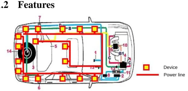
1.2 Features
Device Power line
Fig. 1-1: A generalized model of a power line communication for automotive
the car to supply power and transmit control data to the electric loads such as LED, motor, DC-DC converter. We use capacitive coupling to transmit and receive data and use inductive
coupling to supply power. For the noise interference, we use direct sequence spread spectrum technique to modulate the control data, and we design a transceiver to realize this function.
1.3 Organization
This thesis comprises six chapters. The motivation and features are described in this chapter. Chapter 2 describes the background studies. It starts with an overview of the basic
serial link and other basic knowledge. Then, we introduce the architecture of the clock and data recovery (CDR). Finally, we introduce the direct sequence spread spectrum and its
method for data recovery.
Chapter 3 addresses the idea of our proposed CDR and analyzes the system-level
behaviors of the CDR. We built the transmitter and the receiver for the system behavioral simulation and discuss the effect of jitter and frequency error. Chapter 4 depicts the
implementation of sub-circuits of the transmitter and the receiver. We use SPICE to simulate and verify that it can function well.
Chapter 5 shows the realization on the FPGA and PCB. We use FPGA to realize the transmitter and receiver and backend control circuit. The LEDs, motors, buck converters and
other front-end discrete components are realized on the PCB. We connect the system to the power line and demonstrate the controlling of the LEDs, motors and buck converters. Finally,
Chapter 2
Background Studies
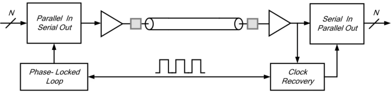
2.1 Basic Serial Link [5, 6]
The concept of serial communication is the process of sending data one bit at a time, sequentially, over a communication channel or computer bus. This is in contrast to parallel
communication which several bits are sent at a time over several parallel channels or buses. A generalized model of serial communication is illustrated in Fig. 2-1. It consists of a transmitter,
a communication channel, and a receiver. The transmitter end contains a serializer, a phase-locked loop (PLL), and an output driver. The PLL supplies the multi-phase clock to the
serializer which serializes the parallel data bits into one serial sequence. The output driver will change the shape of data according to the channel and output the data. The receiver end
contains an input amplifier and a clock recovery circuit and a deserializer. The input amplifier receives the data and restores it. The clock recovery circuit extracts the clock from the input
data and retimes the input data. The data is deserialized into parallel form by a deserializer.
Phase- Locked
Loop RecoveryClock
Parallel In Serial Out N Serial In Parallel Out N
Fig. 2-1: A generalized model of a serial link
2.1.1. Jitter Analysis
Jitter is the time domain behavior of phase noise. It represents the deviation of the zero crossing from their ideal position. In Fig. 2-2, x1 (t) represents the ideal signal and x2 (t)
represents the actual signal. To quantify jitter we can measure the deviation of each positive or negative transition point of x2 (t) from its corresponding point in x1 (t), i.e., ΔT1, ΔT2, etc.
T0 ΔT1 ΔT2 x1 ( t ) x2 ( t ) (a) T1 T2 T3 T1 (b)
Fig. 2-2: (a) Cycle-to-cycle jitter, (b) variable cycles.
This type of jitter is called absolute jitter. Since the deviations are random, we measure a
very large number of ΔT's and determine the root mean square (RMS) value of absolute jitter as: , lim 2 2 2 abs rms N 1 2 N 1 T T T T N (2.1)
Another type of jitter is called cycle-to-cycle jitter. It is obtained by measuring the difference between every two consecutive cycles of the waveform and taking the RMS value:
, lim 2 2 2 cc rms N 2 1 3 2 N N 1 1 T T T T T T T N (2.2)
Absolute and cycle-to-cycle jitters are commonly used to characterize the quality of the signals in the time domain. A third type of jitter is called period jitter. It is defined as the
deviation of each cycle from the average period of the waveform,T :
, lim 2 2 2 p rms N 1 2 N 1 T T T T T T T N (2.3)
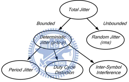
Generally speaking, the total jitter has two components: deterministic jitter (DJ) and random jitter (RJ), as shown in Fig. 2-3.
Total Jitter
Deterministic
Jitter (p-to-p) Random Jitter (rms)
Bounded Unbounded
Period Jitter Duty Cycle Distortion Inter-Symbol Interference
Fig. 2-3: Components of total jitter
The probability density function (PDF) of deterministic jitter is non-Gaussian. So it has
bounded peak-to-peak value. There are three types of DJ: periodic jitter, inter symbol interference and duty cycle distortion. The PDF of random jitter is Gaussian. So it is
unbounded. It is often generated by different noise sources such as thermal noise, power supply noise, substrate noise, etc. Random jitter is characterized by RMS value because it
takes a long time to obtain the peak-to-peak value to achieve statistical significance.
Multiple random jitter sources can be added in an RMS fashion. But it needs a
peak-to-peak value to be added to the deterministic jitter to obtain total jitter. Although the Gaussian statistics imply infinite peak-to-peak value, we can use the probability of data error
to transform RJ to DJ. For example, if the specification of error is 10-12, then the RMS value of RJ multiplies 14.1 is the peak-to-peak value of RJ. The conversion between RMS and
peak-to-peak value of RJ are illustrated in table 2.1 Table 2.1
Probability of Data Error N= Peak-to-Peak /RMS
10-12 14.1
10-13 14.7
10-14 15.3
10-15 15.9
2.1.2. Jitter Transfer
Jitter transfer function of a device represents the output jitter as the input jitter is varied
at different rates. It is defined as the ratio of jitter on the output to the jitter applied on the input of the device under different frequency. It can quantify the jitter accumulation
performance of data retiming devices. Fig. 2-4 shows the jitter transfer mask for OC-192.
2.1.3. Jitter Tolerance
Jitter tolerance specifies how much input jitter a device must tolerate without increasing the bit error rate. For example, the Fig. 2-5 shows the mask of jitter tolerance for OC-192. It
indicates that the system must retime the input data correctly if the input data jitter is over 15UI when the jitter frequency is less than 2.4 KHz.
Fig. 2-5: Jitter tolerance mask[1]
2.1.4. Bit Error Rate (BER)
Bit error rate is an index for the system performance. It represents the reliability of the
link and it defines the data rate of transportation. If the BER is rising above a specified level, it means that the system could not operate properly at the rate. It is calculated as follow:
number of erroneous bits number of transmitted bits
2.2 Architecture of CDR [7]
Fig. 2-6 shows the concept of a clock and data recovery (CDR) circuit. At the receiver side the received data is asynchronous and noisy, so a CDR circuit is used to extract the
information of clock from the input data and synchronize the input data.
D CDR Circuit Q Decision Circuit Input Noisy Data Recovered Clock Recovered Data
Fig. 2-6: Concept of a CDR circuit
2.2.1. PLL-Based CDR
PLL-based CDR is a closed loop system. In general, it refers to and Nth-order system, where N≧2. A general function block of PLL-based type clock and data recovery circuit is
shown in Fig. 2-7[8]. It consists of phase and/or frequency detectors, a charge pump, a loop filter, Phase Detector Charge Pump Low-Pass Filter Voltage-Controlled Oscillator Decision Circuit Din CK Dout
Fig. 2-7: A general function block of PLL-based type CDR [8]
and a voltage-controlled oscillator (VCO). The frequency detectors (FD) are used for the
pull-in process and the phase detectors (PD) are used for the lock-in process. According to the PD structure used in a PLL-based CDR, we can categorize it into linear and binary types [9].
The linear PD proposed by Hogge outputs an Up pulse when the rising edge of the clock leads the transition edge of the data. When the rising edge of the clock lags the transition edge of
D Q Clk D Q Din ΔФ out V Y X
(a) Hogge PD (b) Transfer Curve
π -π
Fig. 2-8: Linear PD proposed by Hogge
the data it outputs a Down pulse. The width of the pulse is the phase difference between the
data and the clock. The phase difference is converted into control voltage of the VCO. The high frequency noise in this control voltage is filtered out by the loop filter. The loop adjusts
the frequency of the VCO by the control voltage until the phase is exactly the same as the input data. The VCO will provide the sampling phase to the decision circuit to retime the
input data. Half-Rate PD Charge Pump LPF 5-GHz VCO MUX Din (10 Gb/s) (10 Gb/s)Dout
Fig. 2-9: A PLL-based CDR with linear PD [8]
Fig. 2-8 shows an example of a CDR with linear PD proposed by Jafar Savoj. It incorporates a half-rate PD to retime and demultiplex the input data. The half-rate PD
produces an error signal and a reference signal. The error signal represents the phase difference. But it is effective only with the reference signal. Because the random nature of the
data and the periodicity of the clock make the average of the error signal which depends on the pattern of the input data. So a reference signal must also be generated to reduce the
dependence by averaging. D Q Clk D Q D Q D Q Din ΔФ out V Y X
(a) Bang-Bang PD (b) Transfer Curve
Fig. 2-10: Bang-bang PD proposed by Alexander
The binary PD proposed by Alexander is also called a bang-bang PD. As we can see from the transfer curve, its output pulse only tells that the clock is lead or lag no matter what
the phase difference amount is. The bang-bang PD is usually used in the all digital structure with digital loop filter or confidence counter and a digitally controlled oscillator. Fig. 2-11
shows an example of a CDR with binary PD proposed by Jafar Savoj.
Low-Pass Filter V/I Converter Half-Rate Half-Rate FD PD V/I Converter Voltage-Controlled Oscillator 0° 45° 90° 135° Din (10 Gb/s) Dout (10 Gb/s) Half-Rate Clock
The system utilizes a half-rate binary PD and a half-rate binary FD to indicate both the phase and frequency difference. Based on the half-rate topology, it reliefs the requirement on
the circuit and retimes the input data inherently. The FD generates an error signal and controls the VCO frequency toward half of the input data. Then the PD takes over. It locks the VCO
phase to the input data and produces a retimed output.
The stability of the feedback system is another issue for the PLL-based CDR. The
tracking bandwidth is limited by the stability of the system and we also have to meet the jitter specification such as jitter tolerance, jitter transfer, etc. In general the loop bandwidth is
usually less than one-tenth of the internal clock frequency.
2.2.2. Oversampling-Based CDR
A blind oversampling CDR is a feed-forward system. Basically, it uses multi-phase of
the clocks generated from PLL to sample the input data. Usually a single data bit will be sampled three times. It is called 3x-oversampling. We can increase the samples to four or
higher to eliminate the transition ambiguity. After oversampling, the transition information of
Multi-Phase Clock Generator
Parallel Samplers Serial Data
Stream SampleStorage
Bit Boundary Detection D ata S ele cti on
Phase Detection Logic
Recovered Data
Fig. 2-12: A block diagram of a blind oversampling CDR [11]
the input data must be detected. We can employ the center-picking or majority-voting method to extract the transition edge of the input data and we can pick the optimum sampling phase of
P1 P2 P3 P1 P2 P3 P1 P2 P3 P1 P2 P3 P1 P2 P3 P1 P2 P3 Input data Sampling Phases Sampled Value 0 1 1 11 1 1 0 0 00 0 0 1 1 11 1 1 0 0 00 0 0 1 1 11 1 1 0 0 Indicate Transition 1 0 0 1 0 0 1 0 0 1 0 0 1 0 0 1 0 Accumulate Transition 6 0 0
Transition Edge judgment P1-P2
Phase Picked P3
Fig. 2-13: An example of phase decision
For example, the data sampled by 3 phases per bit time is shown in Fig 2-13. It decides
the boundary with a portion of a sampled stream. First the neighboring data are XORed. Then the transitions are accumulated. The transition that has the highest accumulated count is the
data transition edge. Then we can choice P3 as sampling phase. We can increase the length of the sampled stream to obtain more accurate results but the storage hardware overhead will
also be increased. Multi-Phase Clock 1:8 Demux Samplers x 24 24
Delay Byte FIFOBit Shifter
S ele ct M ux Decision Logic 3 Sel 8 8 Phase-Picking Logic Din (4 Gb/s) Dout [7:0] (512 Mb/s) Fig. 2-14: An example of oversampling CDR [12]
The phase picking scheme accompanies static phase offset error on each sampling
(0.5UI/OSR), where OSR denotes the oversampling ratio. Although we can increase the OSR to decrease the phase offset but in practical a higher OSR implies high accuracy phase
resolution for each sampling, which is always a challenge. A phase-picking CDR tracks the high-frequency jitter of the input data well while it needs extra circuit such as FIFO buffer to
tracks the frequency error between the input data and the clock. This architecture eliminates the need on the acquisition time but requires more hardware for executing algorithm and
introduces processing latency to the data recovery.
2.2.3. DLL-Based CDR
DLL-based CDR is just like PLL-based CDR but it adjusts the phase of the input data or
the clock. It is a closed loop first-order system. So it is a simplified version of PLL-based architecture. According to the subject of the delay adjustment, it can be divided into two types:
clock interpolation and data-deskew. The clock interpolation architecture can track the input data continuously by the phase rotation scheme. But it needs additional hardware such as
FIFO buffer to overcome the data overflow/underflow problem. For the data-deskew architecture, it adjust the phase of the input data and synchronize it with the phases of the
clock. It is limited by the tuning range of the circuit. So it is only suitable for burst-mode application.
Clock Interpolation
PD PD LPF Digital Loop Filter Multiphase VCO N PFMD Charge Pump Loop A Loop B DFF Retimed Data Data In Frequency Control Phase SelectorFig. 2-15 shows an example of the clock interpolation CDR proposed by Ruiyuan Zhang. It combines the fast acquisition of a phase selection DLL with the low jitter of a PLL. Loop A
is the phase selection loop. It provides fast acquisition with the input data and frequency direction and magnitude estimation for the PLL loop. Loop B, a PLL loop with narrow loop
bandwidth to achieve low jitter. The phase switching is disabled after the PLL acquires the phase lock. The phase selector examines the relationship between the data transitions and the
clock phases from the VCO, and then the circuit selects the sampling phase which is the farthest from the data transitions.
Data-Deskew
Delay Control FSM Confidence Counter Lead Lag Phase Detector Up Dn Data Input Ref. Clock Digitally Controlled Delay LineX0 Xn Recovered Data
Fig. 2-16: A data-deskew CDR proposed by Hung-Wen Lu [14]
Fig. 2-16 shows an example of the data-deskew CDR proposed by Hung-Wen Lu, the
bang-bang PD outputs up and down pulses to give the information of leading and lagging between the clock and the input data. The confidence counter serves as a digital loop filter
accumulates the pulses and filter out the high frequency noise. Then it controls the delay through a finite-state machine (FSM). Finally the input data passes through the delay line and
synchronizes to the clock. This paper proposes an all digital architecture, so it can provide high flexibility and can be synthesizable.
2.3 Direct Sequence Spread Spectrum
2.3.1 Definition of Spread Spectrum
FB PSD NFB Frequency Original Signal Spectrum Spread Signal Spectrum
Fig. 2-17: Power spectral density of spread spectrum signal [15]
Spread spectrum is a technique in which a signal is transmitted on a bandwidth larger
than the frequency content of the original information by modulating a signal. It generally makes use of the noise-like signal to spread the normally narrowband information signal over
a relatively wideband. The receiver correlates the received signals to retrieve the original information signal. The spread spectrum has a lot of benefits, such as: anti-jamming,
anti-interference, low probability of intercept, multiple user random access communication, etc. There are two main techniques of the spread spectrum communication: direct sequence
and frequency hopping. Here we use the direct sequence spread spectrum. We will illustrate it in the following paragraph.
2.3.2 Direct Sequence Spread Spectrum
RF Mod RF Demod PN Code PN Code Data In Despread Data Spreader Despreader(a) Wireless DSSS Sytem
(b) Direct Sequence Modulation Process
-1 +1 1 N +1 -1 “1” “0” -1 +1 PN Code In Out In (Data) Out (Chips) PN Code
Fig. 2-18: DSSS system and modulation process [16]
Direct sequence spread spectrum (DSSS) transmission multiply the data being
transmitted by a noise signal [17]. This noise signal is a pseudorandom sequence of 1 and -1 values at a frequency much higher than that of the original signal. Thereby, it spreads the
energy of the original signal into a wider band. The pseudorandom sequence or pseudo noise (PN) code symbols are called chips. This PN code is generated in a deterministic way but act
like a random signal. Usually it is generated by a linear feedback shift register (LFSR). The transmitted signal resembles white noise. The noise-like signal can be used to reconstruct the
original data at the receiver end. The despread process multiplies it by the same PN code. It calculates the correlation between the transmitted sequence and the local PN code. In a binary
direct-sequence system, a chip is a pulse of a DSSS code. Each chip is typically a rectangular pulse of 1 or -1. It is called chips to avoid confusing them with information bits. The chip rate
is larger than the data rate. That is, one date bit is represents by multiple chips. The ratio is known as spreading factor or processing gain:
chip rate data rate
bandwidth of spread spectrum signal
bandwidth of the information signal
PG
(2.5)
The processing gain also results in enhancing the signal to noise ratio (SNR) on the
channel. When the spreaded signal is transmitted in the channel, it is interfered by narrow band noise. At the receiver end, we use the same PN code to despread the data. At the same
time, the noise will be spreaded and its power is being reduced. So we can attain a better signal to noise ratio.
2.3.3 Code Synchronization
For despread to work correctly, the transmitted and received sequence must be synchronized. It is called code synchronization. It is a process of aligning the PN code
generated from the receiver with the transmitted sequence.
Power Line Tracking
circuits Local PN Code Acquisition circuits Despreader Sync Control Despread Data Code Synchronization PN Code Data In Spreader Fig. 2-19: Code Synchronization [18]
Code synchronization is composed of two parts: code acquisition for the coarse synchronization and code tracking for the fine synchronization [21]. The acquisition process
involves a search through the region of time-frequency uncertainty and determinate that the locally generated PN code and the received sequence are sufficiently aligned within 0.5 chip
done by using a feedback loop which constantly serves to reduce the phase error and retain the alignment. An essential function for timing acquisition, tracking and data recovery is to
calculate the correlation between the local PN code and received sequence. Usually we use matched filter or correlator to calculate the correlation function of the received signal and
local PN code.
Code Acquisition
Typically, the methods for PN acquisition can be classified into serial search and parallel
search. Spreaded Data In Local PN Code Integrate and Dump Threshold Sync control Sync indication Fig. 2-20: Serial search with correlator [19]
As shown in the Fig. 2-20, this is the serial search with correlator. First, the timing of the local PN code has been set and it is correlated with the transmitted sequence. The integrate
and dump block calculates the correlation value over k chips time and dump out the value. The comparator compares the value with a threshold. If the threshold is not exceeded, the
sync control will delay the local PN generator usually by 1/2 chip time. The search process is started again. When the transmitted sequence and local PN code are roughly aligned, the
Multiply and Sum
Delay Line
1 M
PN1 V1
Multiply and Sum
Delay Line
1 M
PN2 V2
Multiply and Sum
Delay Line 1 M PNK VK Spreaded Data In
Fig. 2-21: Parallel search with matched filter [19]
Another one is the parallel search with matched filter. It uses a bank of correlators or
matched filters. Each one has the same PN code with equally spaced timing. When correlating with the transmitted sequence, one of the correlators will exceed the threshold and indicate the
synchronization of both signals. As compared with the serial search method, the parallel search can provide fast acquisition but more hardware is required. Therefore, there is a
time-complexity tradeoff.
Code Tracking
Local PN Code Correlator(Early) Correlator(Late)VCO Loop Filter Spread
Data In
PN+
PN-Phase Error Detector
After acquisition or coarse synchronization, code tracking or fine synchronization takes place. There are two well-known methods: delay-locked loop and tau-dither loop. Fig. 2-22
shows the blocks of the delay-locked loop. It uses two correlators and two PN sequences which they are the same sequence with different phase delay. The early phase is typically 1/2
chip time earlier with respect to the transmitted sequence. The other one is the late phase which is 1/2 chip time delay. Using these two sequences to correlate with the transmitted
sequence and subtract the results. We can get the information of phase error between the transmitted sequence and local PN code. The loop filter is used to filter out the high frequency
noise on the error signal and control the VCO to increase or decrease the frequency smoothly. Therefore, the early and late PN sequence will track the transmitted sequence and let the
phase error approach zero.
Local PN Code
Dither Generator Correlator
VCO Loop Filter Spread
Data In
PN+
PN-Phase Error Detector
Fig. 2-23: Tau-dither loop [20]
The second one is the tau-dither loop. It is the delay-locked loop with only one correlator. The dither generator controls the early and late sequence and let one of them correlated with
the transmitted sequence at each instant of time and then correlates with the result of correlator to get the phase error signal. The next steps are just like the delay locked loops.
Chapter 3
Behavioral Simulation of the Proposed
CDR
3.1 The Proposed CDR
According to the application, the CDR is included in a transceiver of power line communication which processes the data at several MHz. So, if we choose a PLL-based CDR,
we need a low speed VCO at the same as the reference clock. The resolution issue and lock-in time issue makes the PLL-based CDR not suitable for our system. The data-deskew CDR has
the same problems. With oversampling-based CDR, we just need a multi-phase clock generator. The phase decision logic can be implemented as an all-digital structure. It is the
most robust and simplest way to design our system. But the oversampling-based CDR needs a large storage component to eliminate the transition ambiguity or noise to recover the data. So
as to save the hardware overhead, we use the phase rotation method to realize the clock and data recovery. Basically, we use three phases of clock to sample the data. The
3x-oversampling can get enough information of data transition edge with the least phase resolution. Because the data rate is just several MHz, using more phases of clock with higher
phase resolution to sample the data is impractical and uneconomical. From the sampled data, we can get the lead and lag information between clock and data. We rotate the phases of clock
backwards or forwards to get the optimum sampling point of the data. Traditionally, we have to collect the information of data transition of several bits to decide whether the phases should
be shifted or not to avoid the effect of jitter or other noises. Because we use the DSSS modulation scheme, the data has been split into 11 chips. We have to calculate the correlation
value between the chips and the local Barker code. We can get enough information from 11 chips. We can use the correlation value to decide whether we shift the phase of clock. For the
code acquisition and code tracking, we use the same phase rotation scheme to achieve that. The chip rate is 11MHz and the data rate is 1MHz for the preliminary design. We generate 3
phases of the clock of 11MHz for oversampling.
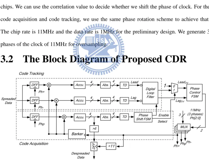
3.2 The Block Diagram of Proposed CDR
DFF DFF DFF Accu. Accu. Accu. Abs. Abs. Abs. TD Barker Digital Loop Filter Enable Phase Control FSM 2 MUXMUXMUX
Ph+ PhpPh-Spreaded Data Ph+ Ph-Php LeadOV LagOV >6 D F F Despreaded Data 11MHz (3 phases) Ph[2:0] 3 Code Acquisition Code Tracking TD TD Lead Lag Phase Shift FSM 0 1 1 Select 4 4 4 4 4 4 ÷11
Fig. 3-1: The proposed CDR
Fig. 3-1 shows the block diagram of the proposed CDR. The system can be divided into two parts consists of code acquisition loop and code tracking loop. Firstly, it uses the punctual
phase (Php) of the clock to sample the input data. The punctual phase is one of the three phases of the clock generator. The sampled data are XORed with Barker code and the
accumulator sums up the outcome and dumps out every bit time. Because all the calculation is done with unsigned operation, the accumulator just only counts the number of times of one.
1: 11 10 9 8 7 6 5 4 3 2 1 0 0: 0 1 2 3 4 5 6 7 8 9 10 11 Transform: 11 9 7 5 3 1 -1 -3 -5 -7 -9 -11
Abs. : 11 9 7 5 3 1 1 3 5 7 9 11
Fig. 3-2: Accumulation and absolution results
Fig. 3-2 shows all the case of accumulation results. For the perfect alignment of the
sampled data and the local Barker code, the results will be 11 or 0 as for data bit 1 or 0. For one chip misalignment or more, the results will be 5 or 6. So we have to set a threshold value
to indicate that whether the sampled data are aligned to the local Barker code. At the same time, we can tolerate that some chips are sampled wrong due to jitter or noise, and still can
recover the original data. But at first we must put the threshold value of data bit 1 and 0 at the same benchmark of comparison. As shown in the Fig. 3-2, we transform the 0 to -1, and
absolutize the results. So now no matter what the data bit is, we can compare the accumulated results with threshold value fairly. We set the threshold value to 3. The accumulated results
must be greater than it to acquire alignment. If the sampled chips do not synchronize to the clock, the select of phase shift FSM will be 0 and let the leadOV be 1. It forces phase control
FSM to shift the phase of clock in order to proceed next synchronization. In code acquisition, we delay the local Barker code 1/3 chip time when shifting the phase of clock. For the worst
case, when the local Barker code is 1 chip time delayed to the sampled chips, it has to shift 33 times of the phase of clock so as to acquire alignment. When the code acquisition is done, the
phase shift FSM will enable the code tracking loop and select the output of digital loop filter as the multiplexer (MUX) output. We take the essence of delay locked loops of basic code
tracking loop. We employ two phases of clock which are the early (Ph+) and late (Ph-) as compared with the punctual phase (Php). Basically, the blocks in the code tracking are the
same in the code acquisition. When there has frequency error between the sampled chips and local clock, the early or late path will fail the threshold test progressively. It implies that the
three sampling phases should be shifted to handle the frequency error. In another way, the situation of frequency error is just like the data drifts forward or backward from the local
clock since the frequency of both does not match. Therefore, we need to shift the phase of clock in the same way as drifting of the sampled chips. Considering the effect of jitter, we
might sample the wrong chips and fail the threshold test and the system would shift the phase of clock. But essentially the system must be capable of dealing with the frequency error and
removing the effect of jitter. According to this, a loop filter must be put into the loop in order that the system can smoothly shift the phase of clock due to frequency error and eliminate the
interference of jitter. The recovery of data is done by comparing the accumulated result with magnitude threshold value 6 directly. Because we have confirmed that the sampled chips and
the local Barker code are synchronized. So now we just need to discriminate the data bit 1 from 0. To sum up, the system performs byte recovery, that is, code acquisition firstly, and
then clock recovery, that is, code tracking, and it uses a D flip-flop to retime the despreaded data.
3.2.1. Correlator of the System
DFF Accu. Abs. TD Barker Ph+ Php Correlator 4 4 Spreaded Data In Fig. 3-3: Correlator
the local Barker code. Actually, it has a 4-bit DFF between the accumulator and the absolute value circuit. So the XOR gate, accumulator, and DFF form a digital integrate and dump
circuit. It dumps out the accumulated results every bit time, or, every 11 chip time. It goes through the absolute value circuit and the threshold detector. The output of the threshold
detector is just 1 or 0 to indicate that whether the accumulation result is greater than the threshold value. If so, the synchronization is completed. Fig. 3-4 shows the behavioral
simulation of the correlator.
Spreaded Data Barker Code XOR output Php Accu. output Abs. output TD output Ph+ Clk
Fig. 3-4: Simulation of correlator
3.2.2. Phase Shift FSM
St0 St1 St2 1/0 1/1 0/1 0/0 Input: TDOUT Output: Enable(Select) 1/1 0/0 Enable Phase Shift FSM Select TDOUTFig. 3-5: Phase shift FSM
The phase shift FSM in the code acquisition loop controls the phase shifting according to
the output of the threshold detector. The state diagram is described that the output of threshold detector has to be 1 two times continuously to set the select and enable signals 1. The local
successively, in case that the noise or jitter causes the system to make wrong decisions. When the burst error happens, it may last more than one bit time. The timing relationship between
the samples chips and the clock must be unchanged. So we design a FSM that the misalignment must occurs two times successively in order to restart the synchronization.
TD1 Clk
Select Enable
1 2
Fig. 3-6: Phase shift FSM
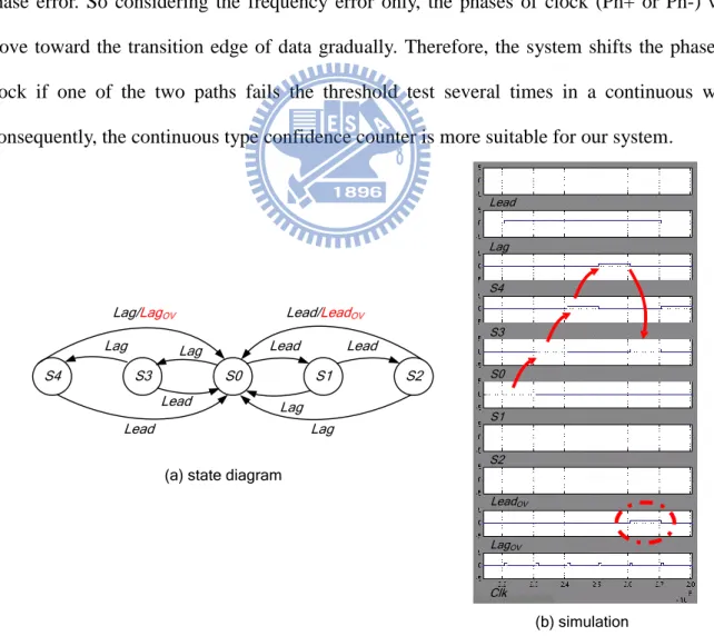
3.2.3. Digital Loop Filter
S0 R S1 S2 S3 S4 S0 S1 S2 S3 S4 R R R L L L L L/LOV R/ROV R R R/ROV R R L L L L/LOV L
(a) Accumulative type
(b) Continuous type
Fig. 3-7: Types of confidence counter
The position of the data transition will move because of the static phase error (frequency error) or dynamic phase error (jitter). The effect induced by the jitter on the sampled chips
the loop filter. There are two types of confidence counter. One is the accumulative type and another is the continuous type. As shown in Fig. 3-7, the initial state of the confidence
counters is set to S0 on both types. R represents the change of the state of the confidence counter to the right; L represents the change of the state of the confidence counter to the left.
The ROV and LOV are the overflow signals indicate that the system should change its state. In the accumulative type, the overflow only happens if three times of R or L are accumulated. In
the continuous type, it happens when R or L occurs three times continuously. Considering the situation where the dynamic and static phase error happens to the system. Because we use
3x-oversampling, the phase resolution is very low. The system can tolerate more dynamic phase error. So considering the frequency error only, the phases of clock (Ph+ or Ph-) will
move toward the transition edge of data gradually. Therefore, the system shifts the phase of clock if one of the two paths fails the threshold test several times in a continuous way.
Consequently, the continuous type confidence counter is more suitable for our system.
S0 S1 S2 S3 S4 Lead Lag Lag Lead/LeadOV Lag/LagOV Lead Lead Lead Lag Lag LeadOV LagOV S2 S1 S0 S3 S4 Lead Lag Clk
(a) state diagram
(b) simulation
3.2.4. Phase Control FSM
C0 C1 C2 LeadOV LagOV LeadOV LeadOV LagOV LagOV Phase Control FSM 3 LeadOV LagOVFig. 3-9: Phase control FSM
The 3-bit output of the phase control FSM control the output of MUX. The states of FSM
are encoded as one-hot-state and used as the output signal. It rotates the clock phases counterclockwise or clockwise depending on whether leadOV or lagOV is 1.
LeadOV LagOV Clk C0 C1 C2
Fig. 3-10: Simulation of phase control FSM
3.2.5. Phase Rotation Scheme
Phase Control FSM 3 MUX MUX MUX Ph+ Php Ph-LeadOV LagOV 11MHz (3 phases) Ph[2:0] 3
The phase rotation is done by a FSM and a MUX, as shown in Fig. 3-12. It can be observed that when Ph2 is shifted to Ph1, the waveform of Ph+ is changed and it advances 1/3
chip time as compared with the original phase. Therefore, if Ph2 is shifted to Ph0, and Ph+ is delayed 1/3 chip time. Besides, Ph+ is used for sampling the data. It is also the clock for
Barker code. The system clock is divided from it as well. Here we must carefully design the MUX of Ph+ to prevent the race problem.
C0 C1 C2 Ph+ Ph0 Ph1 Ph2 C0 C1 C2 Ph+ Ph0 Ph1 Ph2 C0 C1 C2 Ph+ Ph0 Ph1 Ph2
Fig. 3-12: Simulation of phase rotation
3.3 Behavioral Simulation
XORTX
out PRBSrst Barker Code rst CDR Despread DataFig. 3-13: Behavioral simulation of CDR
We use Simulink to execute the behavioral simulation of CDR, the transmitter consists of a Barker code generator, a pseudo random bit sequence generator (PRBS), and a XOR gate.
3.3.1. Chips Delay
PRBS data Recovered data C0 C1 C2 ClkFig. 3-14: Chips delay test
As Fig. 3-14 shows, we delay the input PRBS data to test whether the code acquisition
loop functions well. It shows that the CDR shifts the phases for 26 times, that is, the CDR delays 8 and 2/3 chip time to get synchronization.
3.3.2. Jitter Effect
(a) 0.55UI RJ (b) hist RJ
(a) 0.55UI DJ (b) hist DJ
Fig. 3-16: Deterministic jitter
We produce the effect of jitter on the PRBS data at transmitter end to see whether the
CDR can recover the data correctly. We put 0.55UI random jitter and 0.55UI deterministic jitter on the data. The RJ is in Gaussian distribution and DJ in is uniform distribution. As Fig.
3-17 shows, the CDR still can recover the data and the phase of clock shifted due to jitter.
PRBS data Recovered data C0 C1 C2 Clk
Fig. 3-17: Simulation of RJ and DJ
3.3.3. Frequency Error
transmitter and the clock of the receiver. It causes the data to drift from the sampling clock. So the system must have to shift the phase in the same way in order to fix the error. We set
±1000ppm frequency error at transmitter end. 1000ppm means that there is 1 bit overflow or underflow every 1000 data bits. The run-length in test is 250 data bits, so there will have 1/4
bits overflow or underflow, that is, 2.75 chips overflow or underflow.
PRBS data Recovered data C0 C1 C2 Clk
Fig. 3-18: -1000ppm (clock of the data)
PRBS data Recovered data C0 C1 C2 Clk
Fig. 3-19: +1000ppm (clock of the data)
As we can see from Fig. 3-18 and 3-19, the phases shift clockwisely or
counterclockwisely due to the positive and negative frequency error. When the data is faster than the clock, it will shift counterclockwisely such as C1, to C2 and to C0. We put the jitter
PRBS data Recovered data C0 C1 C2 Clk
Fig. 3-20: +1000ppm with DJ and RJ
3.4 Transceiver Simulation
Send Timing Control XOR 0 1 TXo ut mode1 Preamble Barker Code Counter CDR Sequence Detector Get PISO 32 SIPO 32 RXi nTX
RX
Control Data Control DataFig. 3-21: Transceiver system
The goal of our design is to send 32-bit control signal from the transmitter through the power line of the automobile. Then, we despread the chips and send the data to the driver
circuit. We know that the data length is 32-bit. So the transmission is burst-mode. Therefore every time a set of control data is sent, the CDR needs to resynchronize each time. Preamble
is a sequence of known bits which are sent in each frame. It is used for synchronization. The length of the preamble should be long enough to let the CDR synchronize and recover the
data properly. Consequently, at transmitter end, the preamble is sent before the control data and a counter is used for select the output of the MUX. At receiver end, a sequence detector is
used to detect the pattern of preamble and control the serial-in parallel-out (SIPO) circuit. A timing control circuit between them is used to control the clock of the SIPO circuit, for it
sends out the control data correctly. Fig. 3-22 shows the transmitter end, and fig. 3-23 shows the receiver end.
Mode 1
Preamble
32-bit Control Data
Output of MUX Clk Fig. 3-22: Transmitter Data from TX Data from CDR Clk Get Send P0 P1 P2 P3 1 1 0 1 Fig. 3-23: Receiver
As shown in Fig. 3-22, when mode1 becomes high, the data will be serialed out. In Fig. 3-23, we can see that the CDR is in code acquisition at first. To recover the data, the preamble
must be detected to set the Get and Send signals and trigger the deserializer. P0 to P3 are the first four data bits.
Chapter 4
Circuit Implementation of the
Transceiver
4.1 Transmitter
4.1.1. Barker Code Generator
Barker Code Clk DFF Rst DFF Set DFF Rst DFF Rst DFF Rst DFF Set DFF Set DFF Set DFF Set DFF Set DFF Rst
Fig. 4-1: Barker code
As Fig. 4-1 shows, the Barker code generator is a shift register which the output is
connected to the input. The sequence of Barker code is {00011101101}, it is implemented by setting and resetting the DFF.
4.1.2. Serializer
DFF Clk/32 B[0] B[1] B[30] B[31] 01 DFF DFF 01 DFF 0 1 DFF DFF 0 1 DFF 1 Clk SEL Serial Out Data Fig. 4-2: SerializerThe serializer is a conventional type. It consists of two DFFs and a 2-to-1 MUXs. The
Clk/32 will load 32-bit control data firstly and SEL will be high for a period of Clk and load the data to the input of DFFs. The DFFs serial out the data. The SEL signal is generated from
the circuit shown in Fig. 4-3.
÷32 DFF DFF Clk Clk/32 SEL Clk Clk/32 SEL
Fig. 4-3: Control signal for serializer
4.1.3. Preamble and Counter
The preamble sequence is {1010…….1011}. For the worst case, the synchronization for CDR needs to delay 11 chip times. It is equivalent to 33 times of phase shifting. We
overdesign the sequence length to prevent any problem which may influence the synchronization. Therefore, the length is 42-bit. We use a 6-bit synchronous counter to
generate the preamble and control the MUX and the serializer of the transmitter. We use the least significant bit (LSB) of the counter as the preamble sequence but the last two 11 pattern
trigger the DFF to make the OR output high. So, the preamble will be high all the time. The control signals of the MUX and the serializer are produced in the same way. Both signals will
be high when the counter counts to 43 and 40.
DFF 6-bit Syn. Counter 1 Preamble DFF 1 Mode_1 DFF 1 EN_se
Fig. 4-4: Preamble and counter
4.2 Receiver
4.2.1. Accumulator
The accumulator consists of four half adders and a 4-bit DFFs. The input of accumulator is 1-bit and its output is 4-bit. The carry-out of the half adder connects to the input of the next
half adder except the last one. The DFFs store the sums of the half adders for the next time, their output connect to the input of the half adder.
DFF HA DFF HA DFF HA DFF HA Input Sum Cout Out[0] Out[1] Out[2] Out[3] Clk Fig. 4-5: Accumulator
4.2.2. Absolute Value Circuit
According to the Fig. 3-2, we have already known the input and output of the absolute value circuit. It is a combinational circuit. The truth table is as follow:
1 1 1 0 1 1 1 0 1 0 0 1 1 1 0 0 1 0 1 0 0 0 0 0 X1 0 0 0 0 X2 X3 X4 Y4 Y3 Y2 Y1 1 1 1 0 1 1 1 1 1 1 1 0 0 0 0 1 0 1 0 0 1 1 1 1 0 0 0 0 1 1 0 0 1 0 0 1 1 0 0 0 0 0 0 0 1 0 0 0 1 1 0 0 1 1 0 0 0 1 1 1 1 0 0 1 1 1 1 0
1 4 2 1 2 3 4 2 3 1 4 3 1 2 4 3 2 3 4 2 4 3 Y 1 Y X X X X X X X X X X X X Y X X X Y X X X Fig. 4-6: Absolute value circuit
4.2.3. Threshold Detector
The threshold detector is a 4-bit magnitude comparator. The output of the comparator
will be high when the input is greater than the value we have set. The value is 3 for the code acquisition and code tracking loop and 6 for despread the data.
4.2.4. Confidence Counter
The confidence counter is encoded as an one-hot-state state machine. The input lead and lagsignals control the output of the MUX in order to shift 1 left or right. Fig. 4-7 shows the
Lead/Lag gnd gnd gnd gnd Lag Lead LagOV LeadOV Clk R S R R R R R
Fig. 4-7: Confidence counter
4.2.5. Phase Control FSM
The circuit of the phase control FSM is similar to the confidence counter, we use the
state assignment as its output.
LeadOV/LagOV S0 Clk R R S S1 S2
Fig. 4-8: Phase control FSM
4.2.6. Clock Generator
The chip rate is 11MHz and the data rate is 1MHz. We need to generate three phases of 11MHz. The clock generator is a Johnson counter, it uses 66MHz clock to generate 6 phases
of 11MHz, and we only take 3 of them as the sampling clocks.
DFF D Q Q DFF D Q Q DFF D Q Q Clk Ph0 Ph2 Ph1
Fig. 4-9: Johnson counter
4.2.7. Delay Adjustment
condition. So we design the following circuit to realize the delay signal. DFF DFF DFF 3 3 Ph[2:0] S[2:0] LeadOV S0 S1 S2 Ph0 Ph1 Ph2 Phase Mux Delay circuit Ph+
Fig. 4-10: Delay circuit for Ph+ phase
DFF DFF DFF 3 3 Ph[2:0] S[2:0] LeadOV S0 S1 S2 Ph0 Ph1 Ph2
Phase Mux
Delay circuit
PhpFig. 4-11: Delay circuit for Php phase
4.2.8. Sequence Detector
The sequence detector is used to detect the sync pattern {1011} in the preamble sequence.
Its state diagram is as follows. When it detects the pattern, it will send a Get signal to indicate that the following data are the control signals. The serializer will start to function.
S0: initial S1: get 1 S2: get 10 S3: get 101 S1 1/0 1/1 0/0 S0 S2 S3 0/0 0/0 0/0 1/0 1/0
Preamble from TX
Data from CDR
Clk
Get
Fig. 4-13: Simulation of the sequence detector
4.2.9. Timing Control
The timing control circuit is used to control the divider and the deserializer. At first, the
sequence detector recognizes the preamble and sends the Get signal. Then, the timing control circuit receives the Get signal and enables the divider and the deserializer by the Send signal.
The divider divides the retime clock by 32 and generates Clk/32 used in the deserializer. The deserializer starts to receive the 32-bit control data and send to the backend driver circuit in
parallel form. After sending out the 32-bit control data, the timing control circuit will disable the divider and deserializer. The deserializer stores the control data until the next new control
data is sent. DFF Rst DFF Rst DFF Rst DFF Rst DFF Rst DFF Rst Clk Rst 1 Get Send Clk/32
4.2.10. Deserializer
The deserializer is a conventional one. The simplest structure is suitable enough for our application. DFF DFF DFF DFF DFF DFF DFF DFF DFF DFF DFF DFF Serial In Data Clk Clk/32 B[0] B[1] B[2] B[29] B[30] B[31] Fig. 4-15: Deserializer
4.3 Circuit Simulation of the Transceiver
We use SPICE to perform the circuit simulation of the entire system. Firstly, the channel
is assumed to be ideal. We build up the transmitter and the receiver. Then, we adjust the start time of the transmitter and let the transmitted chips have some delay with respect to the local
Barker code at receiver end. We test whether the phase rotation scheme can recover the data correctly or not. As shown in Fig. 4-17, leadOV has been high for 14 clock period. It means
that the phase rotates 14 times and local barker code is delayed about 4 chip time for the synchronization. Mode 1 Preamble 32-bit Control Data Output of MUX Clk
Data from TX Data from CDR Clk LeadOV LagOV Get Send P0 P1 P2 P3 1 0 1 0
Fig. 4-17: Simulation of the receiver
We can observe that the backend circuit can function well to output the data in parallel.
Next, we change the frequency of clock at the transmitter end to examine if the CDR can shift the phases to correct the frequency error or not.
Data from TX Data from CDR Clk LagOV Get Send P0 P1 P2 P3 1 0 1 0 S0 S1 S2
Fig. 4-18: Simulation of the frequency error
80 data bits. We set the frequency error to 3250ppm. It will underflow 1 chip about every 307.7chips. The total number is about 880 chips. So it will underflow 2.86 chips. As the Fig.
4-18 shows, lagOV happens 8 times as the phase rotates 8 times. It means that the system has shifted 2.67 chips. The direction of rotation is from S0, to S2, and to S1 counterclockwisely.
Chapter 5
Realization of the System on FPGA and
PCB
5.1 Realization of the Transceiver
XOR 0 1 TXout mode1 Preamble Barker Code Counter CDR Sequence Detector Get PISO 32 SIPO 32 ΔΣ-DPWM driver 8 RXin
TX
RX
Control Data Driver SignalFig. 5-1: Transceiver with backend control circuit
The whole application is shown in Fig. 5-1. The purpose is to use the delta-sigma digital
pulse width modulator (ΔΣ-DPWM) to generate PWM signal to control the Power MOS switches. The switches are used to control electric motors, LEDs, or buck converters. The
control. These three components have their own operation frequency. Under this frequency, we can change the on-time duty or PWM of motors or LEDs to control the on-off cycling
frequency, on-off duty cycle or dimming. The input of backend control circuit is 32-bit. The data transmission method is through the existing power line on the car to deliver the data. We
use DSSS modulation to spread data into chips in order to decrease the noise interference. Basically a transmitter and a receiver for DSSS are what we need. Therefore, in order to
realize this idea, we build a prototype using FPGA and discrete components on a bread board.
XOR TXout PRBSrst Barker Coderst CDR Despread Data XOR 0 1 TXout mode1 Preamblerst PRBSrst Barker Coderst Counter rst
CDR Sequence Detector Get
(a) Test of data recovery
(b) Test of detection of preamble
Fig. 5-2: Test for CDR
As shown in Fig. 5-2, we use the pseudorandom bit sequence (PRBS) encoded by barker code to test whether the CDR can despread the chips correctly. And then, we put the preamble
signal before the PRBS data to test the sequence detector. When it receives the recovered data and detects the preamble, it sends out the Get signal to indicate the detection. Besides, we use
PRBS input Recovered data Recovered clock
Fig. 5-3: Test of data recovery
PRBS input
Recovered data Get signal
Fig. 5-4: Test of detection of preamble
Fig. 5-3, 5-4 shows that the system can detect the preamble signal and recover the data correctly. Therefore, the transmitter and receiver can function well.
5.2 SERDES and Backend Control Circuit
Now we add a serializer to the transmitter and a deserializer and the ΔΣ-DPWM control circuit to the receiver, as shown in Fig. 5-5. The simulation procedure is as follows. Set the
32-bit control signal and the transmitter serial out the preamble and the control data. Both of them are encoded by Barker code. Next, the CDR recovers the data and SIPO sends out the
32-bit data in parallel. Finally, the backend control circuit produces the desired PWM control signal. Besides, we use the power line as the transmission channel. Here the DC 12V has not
plugged in yet.
TX Control Data Switch RX
Fig. 5-5: Test of SERDES and backend control circuit
Power line
RX
TX
(a) On-time 50% (b) PWM 50%
Fig. 5-7: On-time 50% and PWM 50%
(a) On-time 25% (b) PWM 75%
Fig. 5-8: On-time 25% and PWM 75%
(a) On-time 75% (b) PWM 25%
Fig. 5-9: On-time 75% and PWM 25%
![Fig. 2-4: Jitter transfer mask[1]](https://thumb-ap.123doks.com/thumbv2/9libinfo/8471735.183561/17.892.154.756.515.1107/fig-jitter-transfer-mask.webp)
![Fig. 2-9: A PLL-based CDR with linear PD [8]](https://thumb-ap.123doks.com/thumbv2/9libinfo/8471735.183561/20.892.130.795.522.936/fig-pll-based-cdr-linear-pd.webp)
![Fig. 2-15: A clock interpolation CDR proposed by Ruiyuan Zhang [13]](https://thumb-ap.123doks.com/thumbv2/9libinfo/8471735.183561/24.892.194.735.895.1094/fig-clock-interpolation-cdr-proposed-ruiyuan-zhang.webp)
![Fig. 2-17: Power spectral density of spread spectrum signal [15]](https://thumb-ap.123doks.com/thumbv2/9libinfo/8471735.183561/26.892.180.766.230.677/fig-power-spectral-density-spread-spectrum-signal.webp)
![Fig. 2-22: Delay-locked loop [20]](https://thumb-ap.123doks.com/thumbv2/9libinfo/8471735.183561/30.892.229.737.861.1107/fig-delay-locked-loop.webp)