國 立 交 通 大 學
光 電 工 程 研 究 所
碩士論文
氮化銦鎵/氮化鎵多重量子井發光二極體之特性與內
部量子效率研究
Study on internal quantum efficiency and characteristic
of InGaN/GaN multiple quantum well light emitting
diode
研究生:柯智淳
指導教授:郭浩中 教授
盧廷昌 教授
氮化銦鎵/氮化鎵多重量子井發光二極體之電特性與內部量子效率研究
Study on internal quantum efficiency and characteristic of InGaN/GaN
multiple quantum well light emitting diode
研究生:柯智淳 Student: Chih-Chun Ke 指導教授:郭浩中 教授 Advisor: Prof. Hao-Chung Kuo
盧廷昌 教授 Prof. Tien-Chang Lu
國 立 交 通 大 學
光電工程研究所
碩 士 論 文
A Thesis
Submitted to Institute of Electro-Optical Engineering
College of Electrical Engineering
National Chiao Tung University
in Partial Fulfillment of the Requirements
for the Degree of
Master
In
Electro-Optical Engineering
June 2008
氮化銦鎵/氮化鎵多重量子井發光二極體之特性與內部量子效率研究 研究生:柯智淳 指導教授: 郭浩中教授 盧廷昌教授 國立交通大學光電工程研究所碩士班
摘要
本論文中,我們利用有機金屬氣相沉積法成長在不同的藍寶石基板上,前者 為成長在圖案化藍寶石基板(Patterned sapphire substrate, PSS)之氮化銦鎵/氮化鎵 (InGaN/GaN)多重量子井(Multiple quantum well, MQW),後者為成長在一般藍寶石 基 板 。 我 們 利 用 光 激 發 螢 光 (Photoluminescence, PL) 、 電 激 發 螢 光 (Electroluminescence, EL) 、 以 及 Advanced Physical Models of Semiconductor
Devices (APSYS)模擬軟體等進行樣品的光學與電特性分析。
我們藉由變功率光激發螢光和低溫電激發螢光量測去探討低溫和室溫時,影 響 氮 化 銦 鎵 / 氮 化 鎵 多 重 量 子 井 發 光 二 極 體 內 部 量 子 效 率 (Internal quantum efficiency, IQE)之物理機制,發現氮化銦鎵/氮化鎵多重量子井發光二極體之內部
量子效率會隨著雷射激發功率而變化,主是受到量子井內之非輻射複合中心以及 量子井內之量子侷限史塔克效應(Quantum confined Stark effect, QCSE)與能帶填 滿效應(Band filling effect)所影響。在本研究中,也利用了理論模型去計算內部量 子效率,計算得到的內部量子效率與實驗結果幾乎吻合。 另外由低溫電激發螢光量測,我們發現當在低溫高電流注入時,電洞會因為 溫度變化造成的載子濃度以及遷移率下降,造成電洞在量子井中的分布不均勻, 且因為電洞的遷移率下降,造成更多的電洞無法有效的注入到量子井中而累積在 靠近p-GaN的量子井中,另外也由於量子井中電洞的不足,造成更多的電子會產 生溢流現象,導致內部量子效率在高電流下會產生效率遽降的情況。
Study on electrical characteristic and internal quantum efficiency of
InGaN/GaN multiple quantum well light emitting diode
Student : Chih-Chun Ke Advisor: Prof. Hao-Chung Kuo
Prof. Tien-Chang Lu
Institute of Electro-Optical Engineering
National Chiao Tung University
Abstract
In this study, we studied two kinds of structures grown by metalorganic chemical
vapor deposition (MOCVD). The samples of InGaN/ GaN MQW ultraviolet light
emitting diode (UV LED) were grown on c-plane patterned and conventional sapphire
substrate. The photoluminescence (PL), low temperature electroluminescence system
(LTEL) and Advanced Physical Models of Semiconductor Devices (APSYS) were
performed to investigate the optical and electrical properties of the grown samples.
This research intends to investigate the physical mechanisms of excitation power
and injection current dependent internal quantum efficiency (IQE) in InGaN/GaN
MQW LEDs at 15 K and 300 K for PL and 30 K and 300 K for EL. The dependence
of the IQE on excitation power density has been observed, we confirmed the variation
of IQE with increasing excitation power is due to the coulomb screening of quantum
confined Stark effect (QCSE) and band-filling effect in InGaN/GaN QW. Moreover,
the nonradiative recombination has to be taken into account at lower excitation power.
coincides with our experimental results.
From the low temperature electroluminescence measurement, the hole
concentration distribution is not uniform which can be attributed to the hole mobility
decreased at low temperature resulting in hole couldn’t transport to the later QW
effectively. Under this condition where thermal generation of holes is insufficient and
injected electrons continuously deplete holes, some of the injected electrons reach the
p-GaN and exit the system without being able. Consequently, the results verified the
誌謝
在打這篇誌謝文的同時,真的有要畢業的感覺。每次在暗房裡跟儀器奮戰到 深夜,每次報告前緊張的反覆演練,現在想起來,好像是昨天才發生的事情。在 這裡,我要感謝在我碩士兩年生活中的許多人,在我遇到困難時對我伸出援手, 在我遇到問題時不吝幫我解答,使我可以順利的完成我的碩士學位。 首先,我由衷的感謝王興宗老師的指導,老師做學問認真的態度深深地影響 我,而在每次報告時老師的殷切叮嚀,我都有牢記在腦海裡;感謝郭浩中老師在 我實驗上遭遇困難時,給予我幫助,以及感謝老師平時對我的鼓勵,使我遇到挫 折時能更勇敢的面對;感謝盧廷昌老師的指導,使我能夠有許多想法去解決實驗 上所遇到的問題。 感謝清華學長,平常Meeting上的指導以及對研究上的規劃和叮嚀,每當我 開始怠惰,總是有學長在旁邊鞭策,以及研究上給予的幫助;感謝明華學長,我 總追著你問很多光學儀器與光學實驗的問題,每次你都不厭其煩的幫助我,也不 時會對於實驗上提供不少想法,因為你和清華學長的協助,我才能更順利的完成 我的實驗。感謝明權學長和瑋婷學妹,最後的低溫EL實驗,若沒有你們的幫忙, 我自己一個人應該會更辛苦,和你們一起做實驗真的蠻快樂的,由衷的謝謝你 們。感謝政暐同學,從大學專題到碩士,在實驗上的問題總是會和你一起討論, 也常常會跟你抱怨實驗的不順利,謝謝你平常對我的鼓勵;感謝小馬、阿綱、治 凱、勁生、玫君、睿中、啄木、尚樺等碩二的同學,因為你們而讓我的碩士生活 更多采多姿。感謝小昕和依嚀學弟妹,常常陪著我做實驗到很晚;感謝永吉學弟, 總是去麻煩你模擬上的問題,對於模擬的理論也從你那學到很多 感謝所有的學長學弟妹們,每當我做實驗沒空吃飯時,總是會有人幫忙買飯 和飲料,每當實驗做到很辛苦時,總是有人相伴聊天,實驗室的笑聲總是會讓我 感到很開心,跟著大家一起吃飯聊天總讓我會忘掉實驗上的辛苦。 最後謝謝我的家人,感謝我的爸爸媽媽支持,讓我順利完成學業,謝謝你們。Content
摘要………i Abstract...ii 致謝………...iv Content...v List of Tables...vii List of Figures...viiiChapter 1 Introduction
1.1 Development of Nitride-Based Light-Emitting Diodes………..11.2 Characteristic of Nitride-Based Ultraviolet Light Emitting Diodes………...2
1.3 Motivation………...5
Chapter 2 Properties of Ⅲ-Nitride semiconductor
2.1 Internal quantum efficiency (IQE)………...92.2 Light extraction efficiency (LEE) and external quantum efficiency (EQE)…...11
2.3 Properties of LED grown on patterned sapphire substrate…………..….……….12
Chapter 3 Experimental instrument and setup
3.1 Sample structure and Fabrication..………163.2 Photoluminescence (PL) ………...16
3.3 Time-resolved photoluminescence (TRPL) and IQE measurement system...18
3.4 Low temperature electroluminescence (LTEL)…..………19
Chapter 4 Excitation power dependent and theoretical model of
calculation IQE in InGaN/GaN multiple quantum wells
grown on patterned sapphire substrate
4.1 Introduction.………..……….244.2 The measurement of internal quantum efficiency of InGaN/GaN UV LEDs...….25
Chapter 5 Analysis of electroluminescence and efficiency droop in
InGaN/GaN multiple quantum wells grown on patterned
sapphire substrate
5.1 Introduction………..……….………...38
5.2 Temperature dependent electroluminescence………..…………...…39
5.3 Injection current dependent electroluminescence at 30 K and 300 K….……...41
5.4 Analysis of injection carrier density dependence EL efficiency and efficiency
droop………...43
5.5 Comparison of PL and EL efficiency……….………46
5.6 APSYS simulation of electron and hole concentration distribution and band
diagram at high injection current…….………...47
Chapter 6 Conclusion
………64List of Tables
Table 4.2.1 Efficiency parameters on PSS and without PSS InGaN/GaN UV LED..36
Table 4.3.1 Nonradiative coefficient A from fitting equation 4.3.4……….37
Table 4.3.2 Experimental IQE and calculation IQE……….37
Table 4.3.3 Auger coefficient calculation and normal C: 10-30~10-34 cm6/s…………37
List of Figures
Fig. 1.1 Benchmark of UV LED in the wavelength range from 370 to 410 nm…...8
Fig. 2.3.1 Top and cross-sectional view SEM images of a PSS by wet etching…….15
Fig. 2.3.2 Schematic illustration of increased light extraction efficiency…………..15
Fig. 2.3.3 SEM morphologies of PSS ………15
Fig. 3.1.1 The schematic drawing of sample structure………...21
Fig. 3.1.2 The schematic drawing of fabrication processes of UV LED………21
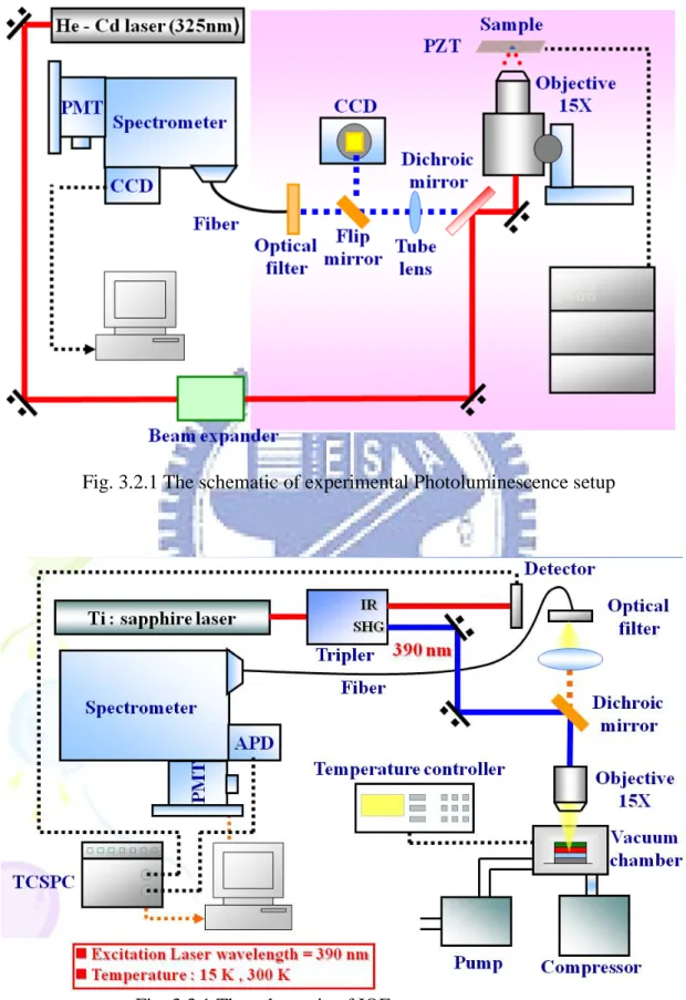
Fig. 3.2.1 The schematic of experimental Photoluminescence setup……….22
Fig. 3.3.1 The schematic of IQE measurement system………..22
Fig. 3.4.1 The schematic of low temperature electroluminescence………23
Fig. 4.2.1 IQE as a function of carrier density at 15 K and 300 K……….34
Fig. 4.3.1 Generation rate G as a function of integrated PL intensity (IPL)………...35
Fig. 4.3.2 Internal quantum efficiency as a function of carrier concentration n…….35
Fig. 4.3.3 Emission power as a function of current density, different slopes can be attributed to different terms dominating the rate equation……….36
Fig. 5.2.2 Temperature dependence of the EL spectra for InGaN/GaN UV LED at injection currents of (a) 0.1 mA, (b) 1 mA, and(c) 20 mA………50
Fig. 5.2.3 Temperature dependence of the EL efficiency at 0.1mA………...51
Fig. 5.2.4 (a) Schematic drawing of temperature dependence EL efficiency (b) Temperature dependence forward voltage at 0.1mA……….51
Fig. 5.2.5 Schematic drawing of effective localized states and defect states……….51
Fig. 5.2.6 Temperature dependence of the EL efficiency at 20mA………52
Fig. 5.2.7 (a) Schematic drawing of temperature dependence EL efficiency (b) Temperature dependence forward voltage at 20mA………..52
Fig. 5.3.1 Current dependence of the EL efficiency at 30K (b) Current dependence
forward voltage at 30K………...53
Fig. 5.3.2 (a) Schematic drawing of current dependence EL efficiency……….53
Fig. 5.3.3 Current dependence of the EL efficiency at 300 K………54
Fig. 5.3.4 (a) Schematic drawing of current dependence EL efficiency (b) Current
dependence forward voltage at 300 K………54
Fig. 5.4.1 (a) An equivalent circuit to represent the four current components: leakage
nonradiative current ID2 by diode D2, and carrier-overflow current IR2
current IR1 by resistor R1, radiative current ID1 by diode D1, by resistor R2
with a switch. (b) EL efficiency as a function of current in the low-current
range………...55
Fig. 5.4.2 Temperature dependent EL efficiency as a function of injection current of
InGaN/GaN UV LED on conventional sapphire substrate………56
Fig. 5.4.3 Temperature dependent EL efficiency as a function of injection current of
InGaN/GaN UV LED on PSS………56
Fig. 5.4.4 EL efficiency as a function of .injection current at 77 K and 300 K……..57
Fig. 5.5.1 EL and PL efficiency as a function of .injection current at low temperature
and room temperature……….57
Fig. 5.5.2 Schematic drawing of carrier transport at low and high injection current.58
Fig. 5.5.3 Efficiency droop mechanisms at low and high injection current………...58
Fig. 5.5.4 EL Efficiency as a function of injection current of InGaN/GaN UV LED
on PSS and conventional sapphire substrate……….59
Fig. 5.5.5 Schematic drawing of electron and hole concentration distribution at low
and high injection current………...59
Fig. 5.6.1 I-V curve of simulation with different hole concentration and mobility…61
Fig. 5.6.2 Electron and hole concentration distribution at high injection current…..61
Fig. 5.6.3 Radiative recombination at high injection curret of InGaN/GaN MQW...62
Chapter 1 Introduction
1.1 Development of Nitride-Based Light-Emitting Diodes
In recent decades, the III-nitrides InN, GaN, and AlN related alloys become an
interesting class of wide bandgap materials and play an important role in
semiconductor devices [1-7], especially for optoelectronics [1-3] as well as
electronics. Since the wurtzite polytypes of III-nitrides form a continuous alloy
system whose direct bandgap ranging from 0.7 eV for InN [8], to 3.4 eV for GaN, and
to 6.2 eV for AlN [9], the optical devices using III-nitrides could be activated at
wavelength ranging from red, green, blue, to deep ultraviolet. This phenomenon is
quite different from other III-V materials systems based on GaAs, AlAs, InAs, GaP
and related alloys. In addition, the III-nitrides materials are expected to be superior to
the counterparts made of Si and other III-V materials for high-temperature and
high-power applications [4-7].
The first blue light-emitting diode (LED) using III-nitrides materials was
fabricated by J. I. Pankove et al.[10] with an metal-i-n structure in 1972. Since that,
related research is going on continually. However, progresses have been limited
because of highly background n-type concentration resulting from the native defects
commonly thought to be nitrogen vacancies and residual impurities such as Si and
appropriate substrates for epitaxial growth. Until late 1980s, H. Amano et al. [11, 12]
discovered a very useful application of a low-temperature buffer layer and developed
low-energy electron beam interaction (LEEBI) techniques to obtain better GaN
epilayer and conductive p-type GaN, initiated a new strong interest in this research
field. Finally, the first GaN-based blue LED constructed of a real p-n junction was
achieved, which had greatly improved in the device performance. However, the
acceptor concentration of p-type GaN is still too low such that the application of these
materials is still unreliable. After that, S. Nakamura et al. [13] achieved better
conductive p-type GaN material by introducing a simple thermal annealing procedure
in nitrogen ambient (≧ 750 ℃). The thermal annealing process represent that an
easy, reliable, and conventional method for obtaining a high conductively p-type GaN.
With these technique developments and achievements, the full-color semiconductor
lighting age has become a reality.
1.2 Characteristic of Nitride-Based Ultraviolet Light Emitting Diodes
GaN-based ultraviolet light emitting diodes (UV LED) tend to be less efficient as
the emission wavelength decreases. It is well known that high efficiency radiative
recombination in dislocated blue and green InGaN multiple quantum wells LEDs has
fluctuation in the InxGa1-xN/GaN quantum wells [14-17]. For UV LEDs, the InN mole
fraction in the InGaN well is lower than that of the blue or green ones. Since phase
separation may does not occur at low In composition [18], it is proposed that less
localized states leads to lower external quantum efficiency of UV LED. T. Mukai and
S. Nakamura performed a comparative study on GaN and InGaN UV (360-380nm)
LEDs grown on sapphire substrate and epitaxially laterally regrown GaN substrates
(ELOG), respectively [19].
Based on the quantum confinement investigation of the GaN-based LEDs,
localized state formed by composition fluctuation in the quantum wells was still
considered a key factor for high quantum efficiency. The effect of dislocation density
on the external quantum efficiency of UV LEDs supports the postulate as well. On the
other hand, carrier overflow, particular in the conduction band, can also be the origin
of low quantum efficiency from a theoretical point of view because the potential well
of an UV LED is much lower than that of its blue and green counterparts. It has also
been reported that band-to-band instead of localized state emission is the dominant
emission mechanism in AlInGaN/InGaN UV (~ 420nm) LEDs [20]. Therefore,
dislocation density and carrier confinement have become very important to improve
the light performance of UV LEDs.
wavelength range from 370 to 410 nm. From the benchmark, it can be deliberated that
the UV LED has a vigorous development after 1999. It is worthy to note that the near
UV LED had a great improvement by using lateral epitaxy on patterned substrate
(LEPS) in 2001 [21]. The enhancement of output power is attributed to the reduction
of dislocation density and light extraction by the patterned substrates. It is well known
that the nitride-based visible optoelectronic devices, grown along the polar [0001]
c-direction, are characterized by the presence of polarization induced electric fields in
the multiple quantum wells (MQWs). These electric fields, caused by both
discontinuities in spontaneous and piezoelectric polarization at heterointerfaces, lead
to the quantum confined Stark effect (QCSE), which would cause charge separation
between holes and electrons in quantum wells and lower radiative recombination
probability [22, 23]. This is one of the primary reasons why thin quantum wells are
employed in c-plane LEDs. Additionally, the peak emission wavelength of LEDs
grown on c-plane GaN would cause blue-shifted with increasing drive current due to
screening of the internal fields.
Conventional GaN-based LEDs are grown on top of sapphire substrates with a
low temperature GaN or AlN nuclear layer. Although the introduction of low
temperature GaN or AlN nuclear layer could significantly improve the crystal quality
109~1012 cm2 will still remain in the sample due to the large difference in lattice
constant and thermal expansion coefficient between sapphire and GaN. Previously, it
has been shown that one can effectively reduce the threading dislocation density down
to 107cm2 or less by using the so-called epitaxial lateral over growth of GaN (ELOG).
In order to achieve such an ELOG, one need to grow a 2~3 μm-thick GaN epitaxial layer on sapphire substrate first, pattern the sample, and then perform the second
MOCVD growth. In other words, we need to perform the MOCVD growth twice.
Recently, it has been reported that one can also reduce the threading dislocation
density in GaN by growing GaN epitaxial layers on top of patterned sapphire
substrates. By using the patterned sapphire substrates, Tadatomo et al. [24] have
successfully fabricated high output power nitride-based UV LEDs with large external
quantum efficiency. To this end, there are several ways to increase the light extraction
efficiency, including shaping of LED dies [25], flip-chip mounting [26], roughening
of the top LED surface [27],[28], growth on a patterned sapphire substrate [29],[30],
and the use of reflectors [31],[32]. Yet, in each of the above cases, the light extraction
efficiency of UV LEDs becomes lower than that of visible LEDs due to a severe light
absorption by transparent electrodes, bonding pads, and wire bonds in the package.
1.3 Motivation
efficiency as injection current increases. This phenomenon which known as efficiency
droop is a severe limitation for high power devices that operate at high current
densities and must be overcome to enable the LEDs needed for solid-state general
illumination. The efficiency droop is caused by a nonradiative carrier loss mechanism,
which is small at low currents but becomes significant for high injection currents.
Competition between radiative recombination and this droop-causing mechanism
results in the reduction in efficiency as current increases. The physical origin of
efficiency droop remains controversial, and several different mechanisms have been
suggested as explanations, including carrier leakage from the active region
[33][34][35]. Auger recombination [36], junction heating [37], and carrier
delocalization from In-rich low-defect-density regions at high carrier densities
[38],[39]. Carrier leakage in GaInN LEDs generally refers to the escape of electrons
from the active region to the p-type region. These leakage electrons may then
recombine with holes either in the p-type region or at the contacts, dominantly by
nonradiative processes. Necessarily, therefore, fewer holes than electrons are injected
into the active region. These two phenomena that escape of electrons form the active
region and reduced hole concentration of any carrier leakage explanation for droop.
Hole injected into the active region may be the limiting factor, possibly due to the low
barrier also for holes. As a result of the low hole injection, current across the device is
dominated by electrons. Devices with p-type active regions which should increase
hole injection efficiency have been proposed as a solution to this problem.
However, it is not clear which cause the efficiency droops at high current. For
this study, we discussed the temperature dependence IQE as a function of injection
current density clearly. By investigating the excitation power dependence PL intensity
at low and room temperature, we can obtained the value of IQE, Then, we study the
temperature dependence EL intensity as a function of injected current density and
APSYS simulation, the physical mechanisms of current dependent IQE of
InGaN/GaN UV LED has been confirmed.
This thesis is organized in the following way: In chapter 2, we give some
theoretical backgrounds and characteristics about InGaN/GaN MQW structures. The
experimental setups and theory are stated in chapter 3. In chapter 4, we present the
experiment results and discuss for optical properties of InGaN/GaN MQW UV LED
grown on conventional and patterned sapphire substrates. In chapter 5, we show the
experiment results and discuss for physical mechanisms of temperature dependence
IQE as a function of injection current density in InGaN/GaN UV LEDs. Finally, we
Chapter 2 Properties of Ⅲ-Nitride semiconductor
In this chapter, we show the definition of internal quantum efficiency (IQE),
light extraction efficiency (LEE), and external quantum efficiency (EQE). Finally, we
show the properties and advantages of InGaN/GaN MQW grown on patterned
sapphire substate (PSS).
2.1 Internal quantum efficiency (IQE)
The active region of ideal LED emits one photon when one electron injected.
Each charge quantum-particle (electron) produces one light quantum-particle (photon).
Thus the ideal active region of an LED has a quantum efficiency of unity. The internal
quantum efficiency is defined as:
e / I h / P ond sec per LED o int injected electrons of number ond sec per region active from emitted photons of number int nt i ν η = =
where Pint is the optical power emitted from the active region and I is the injection
current. Photons emitted by the active region should escape from the LED die. In an
ideal LED, all photons emitted by the active region are also emitted into free space.
Such an LED has unity extraction efficiency. However, in a real LED, not all the
power emitted from the active region is emitted into free space. Some photons may
never emit into the free space. This is due to several possible loss mechanisms. For
on a metallic contact surface and be absorbed by the metal. In addition, the
phenomenon of the total internal reflection, also refereed to as the trapped light
phenomenon, reduces the ability of light to escape from the active region.
Another view point, the internal quantum efficiency in a semiconductor is related
to non-radiative recombination centers. If the radiative lifetime is denoted as τr and the
non-radiative lifetime is denoted as τnr, then the total probability of recombination is
given by the sum of the radiative and non-radiative probability:
nr r
1
1
1
τ
τ
τ
=
+
(2.1.1)The relative probability of radiative recombination is given by the radiative
probability over the total probability of recombination. Thus the probability of
radiative recombination or IQE is given by:
1 nr 1 r 1 r int − − −
+
=
τ
τ
τ
η
(2.1.2)The IQE gives the ratio of the number of light quanta emitted inside the
semiconductor to the number of charge quanta undergoing recombination. Note that
not all photons emitted internally may escape from the semiconductor due to critical
By the above equation, the internal quantum efficiency is determined by the
competition between radiative and nonradiative recombination processes. In this
material system, the radiative recombination rate is affected by the quantum-confined
Stark effect (QCSE) and exciton localization effects. Although the relative importance
of these contributions has been widely studied in recent years, many questions
regarding the emission process still remain.
2.2 Light extraction efficiency (LEE) and external quantum efficiency (EQE)
The extraction efficiency can be a severe limitation for high performance LEDs.
It is quite difficult to increase the extraction efficiency beyond 50% without resorting
to high sophisticated and costly device processes. The light extraction efficiency (LEE)
is defined as: ν ν η h / P h / P ond sec per region active from emitted photons of number ond sec per space free o int emitted photons of number int extraction = = (2.2.2)
where P is the optical power emitted into free space. Considering the refractive
indices of GaN (n = 2.5) and air, for the light escape cone is about 23% due to the
critical angle. Assuming that light emitted from sidewalls and backside is neglected,
surface. The light outside the escape cone is reflected into the substrate and is
repeatedly reflected, then reabsorbed by active layers or electrodes, unless it escapes
through the sidewalls. However, there is much room for improvement of the light
extraction efficiency. For example, roughening of the top LED surface increased the
light extraction efficiency.
Finally, the external quantum efficiency (EQE) is defined as:
(2.2.3)
from the above equation, we can know that the EQE depend on IQE and LEE,
therefore, the improvement of IQE and LEE pay an important role of LED. Recently,
the patterned sapphire substrate is introduced to improve the IQE which is attributed
to reduce the dislocation density and enhance the LEE due light emit to substrate
may reflect and emit into free space.
2.3 Properties of LED grown on patterned sapphire substrate
However, owing to the large mismatch (~14%) of lattice constant [40] and
thermal expansion (~25%) between epitaxial GaN films and sapphire substrates,[41]
high density dislocations ranging from 108~1010 cm-2 degrade the light-emitting diode
(LED) performance profoundly. Thus, growth of GaN with low-density dislocations
extraction ext e I h P ond per LED o injected electron of number ond per space free o emitted photons of number ν η η η int / / sec int sec int = = =
has been a major effort for fabrication of reliable high-efficiency LEDs. By epitaxial
lateral overgrowth (ELOG) with SiNx or SiO2 mask patterned on as-grown GaN seed
crystal, threading dislocations can be significantly eliminated. Although this
overgrowth technique can dramatically improve crystalline quality, the requirement of
two-step growth procedure is time-consuming and easily introduced contaminations.
In recent years, the single growth technique by introducing patterned sapphire
substrates (PSS) has been extensively researched. The simplified growth method can
reduce the threading dislocations and increase the light extraction. The geometrical
shape of the sapphire patterns can effectively scatter or redirect the guided light inside
an LED chip to find escape cones, such as the hemispherical shape made by the dry
etching technique [42] and the inclined c-plane facet of sapphire made by the wet
etching technique [43]. In brief, the patterned sapphire substrate has some benefits:
(1) Reduced the threading dislocation
(2) Single growth process without any interruption
(3) Increases the emitting light extraction efficiency
Fig. 2.3.2 displays the schematic illustration of increased light extraction
efficiency. Another technique is chemical wet etching which is a promising technique
coupled plasma (ICP) used in dry etching. The characteristic inclined crystallographic
facets resulting from wet etching can facilitate superior light extraction efficiency.
Wet-etching causes less damage to the substrate than dry etching does, hence the
sapphire surface damage induced by dry etching can be eliminated. In this study, we
prepared two samples grown on conventional and patterned sapphire substrates. Cross
sectional of SEM micrographs of the patterned sapphire substrate is shown in Fig.
2.2.3. The lens height and diameter of the patterned sapphire are 1.4 and 3.5μm,
respectively. The distance between each lens is 1.0 μm. We can observe the lens
pattern is uniformly arranged and homogeneous size distribution. In the normal wedge
shape pattern, one could reduce the threading dislocation whereas the optical emission
is not enhanced appreciably. On the other hand, by using lens shaped PSS, TD density
can be reduced and also optical emission efficiency could be improved due to internal
Fig. 2.3.1 Top and cross-sectional view SEM images of a PSS by wet etching
Fig. 2.3.2 Schematic illustration of increased light extraction efficiency
Chapter 3 Experimental instrument and setup
3.1 Sample structure and Fabrication
The sample in this study are commercial InGaN/GaN MQW UV LEDs and
grown by metalorganic chemical vapor deposition (MOCVD). The sample in this
study grown on c-plane (0001) sapphire substrates and patterned sapphire substrate
(PSS), respectively. The sample structure consist 1.5μm undoped n-GaN, a 2μm
Si-doped n-type GaN, and an unintentionally doped active layer with InxGa1-xN/GaN
MQWs, and a 20nm p-AlGaN electron blocking layer (EBL), a 50nm p-Al0.2Ga0.95N,
and 20nm Mg-doped p-type GaN. The doped concentration of n- and p-type GaN is
nominally 5 × 10¹⁸ and 1 × 1019 cm-3, respectively, the MQWs layer comprise 6
periods InGaN well (~2.5 nm) and GaN barrier (~1.5 nm). The sample structure is
shown in Fig. 3.1.1. The fabrication processes of InGaN/GaN UV LED show in Fig.
3.1.2. In this study, we is interested in the reduction of dislocation density of
InGaN/GaN UV LED on PSS which may affect the internal quantum efficiency and
the efficiency droop at high current, hence, we will study the relation between defects
and physical mechanisms of quantum efficiency.
3.2 Photoluminescence (PL)
properties of the materials because of its nondestructive characteristics. PL is the
emission of light from a material under optical excitation. The laser light source used
to excite carriers should have larger energy band gap than the semiconductors. When
the laser light is absorbed within the semiconductors, it would excite the carriers from
the valence band to the conduction band. Then, it produces the electrons in the
conduction band and the holes in the valence band. When the electron in an excited
state return to the initial state, it will emit a photon whose energy is equal to the
energy difference between the excited state and the initial state, therefore, we can
observed the emission peak from PL spectrum.
The photoluminescence spectroscopy is the optical measurement to examine the
quality and optical characteristic of material.First, when we analysis a new compound
semiconductor, we can use PL measurement to know the band gap of the new material.
Second, the intensity of PL signal is contributed to the amount of radiative
recombination in the materials. Therefore, PL measurement can be used to understand
the material quality and the recombination mechanisms of the materials.
The carrier recombination processes occur in many ways in order to reach the
equilibrium. Those processes can be divided into radiative recombination and
nonradiative recombination. We can recognize the radiative recombination easily at
energy.
If there are some defect energy level existed in energy band gap of
semiconductor, they also could contribute to radiative recombination process.
Therefore, we could observe the multiple emission peaks in the PL spectrum, and the
intensity of the emission peaks is related to the contribution of the individual radiative
recombination process.
The schematic setup of our PL system is shown in Fig. 3.2.1. The pumping
source was a multi-mode and non-polarized Helium-Cadmium laser operated on 325
nm with 35 mW. After reflecting by three mirrors, the laser light was focused by a
lens which focal length was 5 cm, to 0.1 mm in diameter and the luminescence signal
was collected by some lens. The probed light was dispersed by 0.32 monochromator
(Jobin-Yvon Triax-320) with 1800, 1200, and 300 grooves/mm grating and the
maximum width if the entrance slit was 1 mm. In order to prevent the laser coupling
with the PL spectrum, we used the long pass filter in front of the entrance slit. In the
temperature-dependent PL measurement, all the samples were placed in the
closed-cycle cryostat with a temperature controller ranging from 20 K to 300 K.
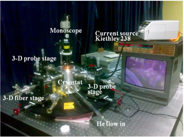
3.3 Time-resolved photoluminescence (TRPL) and IQE measurement system
the dynamical process of photoexcited carriers such as relaxation, radiative,
nonradiative, and localization processes. The transient luminescence intensity
obtained by the data of TRPL is generally expressed by the following equation as a
function of time after excitation:
)
exp(
)
0
(
)
I(
τ
t
I
t
=
−
(3.3.1)The pulsed excitation source for the IQE measurement is provided by the frequency
doubler (2w) or frequency tripler (3w) beams of a mode-locked Ti: sapphire laser (w)
which was pumped by Ar+ laser. The wavelength of Ti: sapphire laser is tunable from
700 nm to 900 nm and the pulse width is 200 fs. The repetition rate of the Ti: sapphire
laser is 76 MHz whose time interval is 12.5 ns. The PL luminescence spectrum was
measured in conjunction with monochromator using gratings whose grooves are 2400
lines/grooves. To direct examine the optical properties of InGaN/GaN MQW LEDs
and avoid the absorption of GaN film, the pumping light source was a frequency
doubled Ti: sapphire laser operated on 370 nm. And all the samples were placed in the
closed-cycle cryostat with a temperature controller ranging from 20 K to room
temperature.
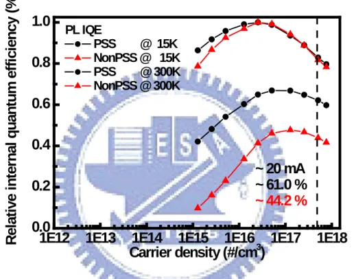
3.4 Low temperature electroluminescence (LTEL)
observe the patterned electrode of sample surface, three axial stages for probe and
fiber to detected the light output, and a cryostat for the cooling system which use the
liquid helium to cooling the chamber. Then, the light detected by a 0.32 m
monochromator (Jobin-Yvon Triax-320) with 1800, 1200, and 300 grooves/mm
grating and the maximum width if the entrance slit was 1 mm. And all the samples
were placed in the closed-cycle cryostat with a temperature controller ranging from 77
K (Liquid helium) to room temperature. Fig. 3.4.1 shows the schematic of low
Fig. 3.1.1 The schematic drawing of sample structure
Fig. 3.2.1 The schematic of experimental Photoluminescence setup
Chapter 4 Excitation power dependent and theoretical model of
calculation IQE in InGaN/GaN multiple quantum wells
grown on patterned sapphire substrate
4.1 Introduction
To improve the performance of InGaN/GaN LEDs, it is very important to know
what physical mechanisms affect the IQE in this material system. Traditionally , the
IQE can be obtained by measuring temperature dependent PL at a certain excitation
condition, and assume IQE is equal to 100 % at low temperature, then the relative
IQE can be obtained at room temperature. However, IQE is well known to be strongly
dependent on injected carrier density, especially in InxGa1-xN MQW system due to the
existence of large internal electrical field and potential fluctuation. Therefore, it is
important to measure and discuss IQE as a function of excitation power density. It is
especially interesting to measure IQE at the carrier density which corresponds to a
certain current injection level in EL measurement, for example 20 mA for a small
junction chip with conventional size. S. Watanbe et al. [44] proposed a method to
determine IQE by performing excitation power density and temperature dependent
PL.
In their study, the variation of IQE of InGaN/GaN UV LEDs grown on PSS and
conventional substrate with increasing excitation power at 15 K and 300 K has been
observed. But they did not say anything more to explain what physical mechanisms
InGaN/GaN UV LEDs and also observed that the IQE changes with increasing
excitation power density. Further, we investigated the difference between excitation
power dependence IQE of InGaN/GaN UV LED on PSS and conventional substrate.
The detailed variation of IQE on different substrates will be discussed later.
4.2 The measurement of internal quantum efficiency of InGaN/GaN UV LEDs
For this study, we used the IQE method which S. Watanabe et al. proposed to
determine the IQE of InGaN/GaN MQW UV LEDs. The internal quantum efficiency
can be calculated by EX EX PL PL PL
E
I
E
I
C
/
/
=
η
(4.2.1)where IPL and IEX are PL intensity and excitation intensity, respectively. EPL and EEX
are PL photon energy and excitation photon energy, respectively. C is a constant
affected by mostly carrier injection efficiency by laser, light extraction and correction
efficiency of PL, and does not depend on either excitation power density or
measurement temperature. First, we measured the excitation power dependent PL
intensity at low and room temperature, and then the relative PL quantum efficiency
curves can be obtained by using equation 4.2.1. And the constant C would be canceled
is independent on temperature or excitation power. From this normalization, the PL
efficiency curves will not depend on carrier injection efficiency by laser, light
extraction and correction efficiency of PL. Therefore, the PL efficiency would be find
out from this model.
In tradition, the IQE is estimated by assuming that IQE is 100 % at low
temperature regardless of excitation power density. However, IQE is strongly
dependent on injected carrier density. Consequently, it is more reasonable to assume
the peak of PL efficiency at lowest temperature is equal 100 %, and then the IQE
curves as a function of excitation power and temperature can be understand.
Moreover, to avoid the absorption of GaN, the frequency doubled femtosecond
pulse Ti: sapphire laser of 370 nm was used to excite sample, the excitation power
density was changed from 0.01 to 15 mW, and calculated injection carrier density is
about 2.0 × 10¹⁵ to 1.6 × 1018 cm-3 by using the equation below:
objective active InGaN GaN GaN active loss R d d f d h P density
carrier *exp( )*(1 exp( )) * * * * ) ( ν φ −α − −α = (4.2.2)
where P is excitation power, hν is energy of incident light, φ is laser spot size, f is repetition rate of laser, dactive is the active layer thickness, αGaN is the absorption of
GaN, αInGaN is absorption of InGaN, R is reflection of sample surface, and Lossobjective
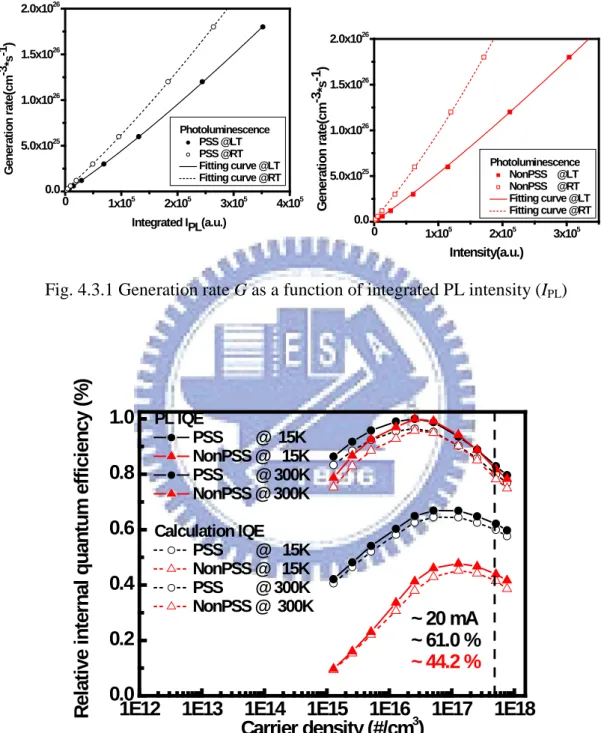
Fig. 4.2.1 shows the IQE of InGaN/GaN MQW UV LEDs as a function of
injected carrier density at 15K and 300 K. We can observe that the IQE increases with
increasing injected carrier density to reach its maximum. As injected carrier density
further increases, then the IQE decreases. The tendency of two efficiency curves at 15
K and 300 K is very similar. But under low injected carrier density region, the IQE
curve at 300 K increases obviously than it at 15 K. The results indicated that the IQE
at 15 K saturated more easily than it at 300 K. The detailed physical mechanisms will
be discussed later.
There are three possible mechanisms to explain excitation power dependence the IQE
at low and room temperature:
(1) Nonradiative recombination centers
For GaN based LED, a large number of dislocation density exist in the device,
and the defects would be occurred nonradiative recombination. Generally, the
nonradiative centers were quenched at low temperature. In our case, as injected
carriers increase, the nonradiative recombination is gradually suppressed, therefore,
the radiative recombination stars to dominate the recombination process, resulting in
the enhancement of IQE, which is observed in Fig 4.2.1. And IQE curve at 15 K
increases not obviously than it at 300 K due to noradiative centers were quenched at
saturated at lower injected carrier density due to the reduction of carriers captured by
nonradiative recombination centers. The results demonstrated that InGaN/GaN UV
LEDs on PSS has better crystal quality and smaller defect density.
(2) Coulomb screening effect
Several research groups have reported that the internal electric field existed in
InGaN/GaN QW structure. This internal electric field through the QW tilts the
potential band and leads to a spatial separation of electrons and holes in the QW [45],
resulting a decreasing in degreed of wave function overlap which is called the QCSE.
The internal electric filed in the QW cam be screened by photogenerated carriers.
Consequently, the QCSE effect become weaker when the carrier density increased,
resulting in the IQE enhanced at low injected carriers region.
(3) Band filling effect of localized states
Due to composition inhomogeneity and monolayer thickness fluctuation Of
InGaN QWs self-organized In-rich region is generated in InGaN active region,
resulting in potential fluctuation of energy bandgap. As injected carrier density
increases further, an occupation of high energy stats of localized centers will be
enhanced. And the band filling effect will make the carriers more easily escape from
localized states to extendend states which decrease IQE.
injected carrier density is 4.7 × 10¹⁷ #/cm3(~20mA) for InGaN/GaN UV LED on PSS
and conventional substrate, respectively. Table 4.3.1 shows the value of IQE and EQE,
and then we calculated the extraction efficiency using the relation equation:
Extraciotn IQE
EQE
η
η
η
=
*
. (4.2.1) We can obtained the extraction efficiency are about 70.5 %, 63.3 % for InGaN/GaNUV LED on PSS and conventional substrate, respectively. Several research groups
demonstrated PSS can reduce the threading dislocations and increase the light
extraction. Our results also indicated that InGaN/GaN UV LEDs on PSS increase the
IQE (and light extraction efficiency.
4.3 Theoretical model of IQE Calculation
In this study, we quote E. F. Schubert et al. [46] proposed theoretical model to
calculate IQE of InGaN/GaN MQW UV LEDs. The three main carrier-recombination
mechanisms in a bulk semiconductor are Shockley–Read–Hall nonradiative
recombination, expressed as An, bimolecular radiative recombination Bn2, and Auger
nonradiative recombination Cn3, where A, B, and C are the respective recombination
coefficients and n is the carrier concentration. Auger recombination affects LED
and the IQE at steady state can be expressed as 3 2
R
G
=
total=
An
+
Bn
+
Cn
(4.3.1)G
Bn
Bn
An
Bn
IQE
2 2 2=
+
=
(4.3.2)and the integrated PL intensity can be expressed as
2
Bn
I
PL=
η
(4.3.3)where is a constant determined by the volume of the excited active region and the total collection efficiency of luminescence. By eliminating n in equation 4.3.1 and
4.3.3, we can express the generation rate in terms of integrated PL intensity
5 . 1 5 . 1 ) ( 1 PL I B C PL I PL I B A G η η η + + = (4.3.4) 5 . 1 3 2 1 IPL P IPL P IPL P G = + + (4.3.5) G P G 2 2 PL PL I I G Bn IQE= = =
η
(4.3.6)The connection between theory and experiment is completed by noting that the
generation rate can be separately calculated from experimental parameters using
ν
α
ν
α
h A R lh A l R spot Laser spot Laser(1 ) P (1 ) P G= − = − (4.3.7)where PLaser is the peak optical power incident on the sample, R (18 %) is the Fresnel
reflection at the sample surface, l (15 nm) is the total thickness of the InGaN QWs,
Aspot (1.96 × 103μm2) is the area of the laser spot on the sample surface, hυ(3.18
eV) is the energy of a 370 nm photon, and. αm-1) is the absorption coefficient of the
In0.1Ga0.9N well at 370 nm.
First, we measured the PL spectrum dependent excitation power, and then the
generation rate (G) curves as a function of PL intensity (IPL) can be obtained by using
equation 4.3.4. We used equation 4.3.4 to fit the experimental data in Fig. 4.3.1, then
we obtained the coefficients P1 =A(Bη)0.5, P2 =1/η, P3 = C/(ηB)1.5. The fitting curves
appear to accurately model our experiments, also shown in Fig. 4.2.1. If one assumes
a value of B at room temperature of 1 × 10⁻¹⁰ cm3/s, the value of carrier
concentration n can also be obtained. By eliminating η from the two coefficients P1
and P2, one can obtain the value of coefficient A finally. The table 4.3.1 shows the
nonradiative coefficient A at low and room temperature. The nonradiative coefficient
A as a function of dislocation density, including values of 8.66 × 10⁵, 1.64 × 10⁶ at
low temperature and 1.28 × 10⁷, 2.45 × 10⁷ s−1 for InGaN/GaN UV LEDs on PSS
and conventional sapphire substrate, respectively. Nonradiative coefficient of without
PSS UV LED is larger than PSS at low and room temperature. Generally,
supports the argument that threading dislocations behave as nonradiative
recombination centers. The results indicated the InGaN/GaN UV LEDs on PSS has
better crystal quality and larger quantum efficiency due to the reduction of threading
dislocation density.
After that, we know the carrier concentration n and P2, so we can be obtained
IQE curves as a function of carrier concentration n in Fig 4.3.2. The calculation of
IQE is very similar to our experimental results. Fig. 4.3.3 shows the emission power
as a function of current density, different slopes can be attributed to different terms
dominating the recombination-rate equation.
We can reproduce the dependence of the internal efficiency on current density, J,
using a simple rate-equation model of the form
3 2
~
An
Bn
Cn
J
+
+
(4.3.8) where n is the QW carrier density and A, B, and C are coefficients for nonradiative,radiative, and (nonradiative) Auger-like recombination, respectively. We thus identify
a high-density QW-internal Auger-like process as the culprit for the high-current
losses observed, with C = 6.03 × 10⁻²⁹ and 1.33 × 10⁻²⁹ cm6/s for InGaN/GaN UV
LEDs on PSS and conventional substrate at room temperature. The value of C is
higher than the normal Auger coefficient (10-30~10-34 cm6/s). And the calculated order
1019 #/cm3). The hole mobility decreased at low temperature resulting in hole couldn’t
transport to the later QW effectively. The results indicated that the carrier distribution
is not uniform in the QW; the carrier density may be attained ~1019 #/cm3 to occur
Auger-like recombination insome QW. Therefore, we demonstrated the Auger-like
effect affect the efficiency droops at high injection current. The efficiency droop may
Fig 4.2.1 IQE of InGaN/GaN LEDs as a function of carrier density at 15K and 300 K.
1E12
1E13
1E14
1E15
1E16
1E17
1E18
0.0
0.2
0.4
0.6
0.8
1.0
PL IQE PSS @ 15K NonPSS @ 15K PSS @ 300K NonPSS @ 300KR
el
at
ive i
n
ter
n
al
q
u
an
tu
m
ef
fi
ci
en
cy (
%
)
Carrier density (#/cm
3)
~ 20 mA
~ 61.0 %
~ 44.2 %
0 1x10⁵ 2x10⁵ 3x10⁵ 0.0 5.0x1025 1.0x1026 1.5x1026 2.0x1026 Photoluminescence NonPSS @LT NonPSS @RT Fitting curve @LT Fitting curve @RT G en er at io n r at e( cm -3 *s -1 ) Intensity(a.u.)
Fig. 4.3.1 Generation rate G as a function of integrated PL intensity (IPL)
Fig. 4.3.2 Internal quantum efficiency as a function of carrier concentration n 1E12 1E13 1E14 1E15 1E16 1E17 1E18
0.0 0.2 0.4 0.6 0.8 1.0 PL IQE PSS @ 15K NonPSS @ 15K PSS @ 300K NonPSS @ 300K Calculation IQE PSS @ 15K NonPSS @ 15K PSS @ 300K NonPSS @ 300K R el at ive i n ter n al q u an tu m ef fi ci en cy ( % ) Carrier density (#/cm3) ~ 20 mA ~ 61.0 % ~ 44.2 % 0 1x10⁵ 2x10⁵ 3x10⁵ 4x10⁵ 0.0 5.0x1025 1.0x1026 1.5x1026 2.0x1026 Photoluminescence PSS @LT PSS @RT Fitting curve @LT Fitting curve @RT G en er at io n r at e ( cm -3 *s -1 ) Integrated IPL(a.u.)
Fig. 4.3.3. Emission power as a function of current density, different slopes can be attributed to different terms dominating the recombination-rate equation
Table 4.2.1 Efficiency parameters on PSS and without PSS InGaN/GaN UV LED
Sample PL IQE (%) Exp. EQE (%) Extraction (%)
PSS NonPSS ~ 61.0% ~ 44.2 % ~43.0% ~28.0% ~70.5% ~63.3%
Table 4.3.1 Nonradiative coefficient A from fitting equation 4.3.4 Sample A (s-1) @ 15K A (s-1) @ 300 K PSS NonPSS 8.66x10⁵ 1.64x10⁶ 1.28x10⁷ 2.45x10⁷
Table 4.3.2 Experimental IQE and calculation IQE
Sample PL IQE (%) Calculation of IQE (%)
15K 300 K 15K 300 K
PSS ~85.9 % ~61.0% ~82.4 % 60.6%
Non-PSS ~85.9% ~44.2% ~82.4% 41.8%
Table 4.3.3 Auger coefficient calculation and normal C: 10-30~10-34 cm6/s
Sample C (cm6/s) @LT C (cm6/s) @RT
PSS 2.48x10⁻²⁹ 6.03x10⁻²⁹
Chapter 5 Analysis of electroluminescence and efficiency droop in
InGaN/GaN multiple quantum wells grown on patterned
sapphire substrate
5.1 Introduction
Recently some research groups have investigated temperature dependence of the
electroluminescence (EL) spectral intensity [47][48][49], which reveals anomalous
EL quenching at lower temperatures below 100 K. It is found that the anomalous
temperature dependence of the EL efficiency is caused by interplay of the carrier
capture and the IQE. One interesting observation of the InGaN/GaN QW diodes so far
is that the EL efficiency dramatically decreases when the diode temperature is
decreased below 100 K, where the improved EL efficiency is generally expected due
to the decreased nonradiative recombination processes. One of the anticipated genuine
causes for the low temperature EL quenching may be ascribed to the deep Mg
acceptor level of 170 meV in p-GaN [50], which can be deactivated at lower
temperatures below 100 K. Therefore, holes are failed to be injected into the QW
active region from the p-GaN layer, especially when the electron blocking p-type
AlGaN barrier is introduced. For this study, detailed physical mechanisms for the EL
enhancement effects under the forward bias conditions have been confirmed. And we
have investigated the carrier transport mechanisms particularly by using APSYS
5.2 Temperature dependent electroluminescence
Temperature dependence of the EL spectra at various injection current levels has
been measured between 30 and 300 K. Three-dimensional (3D) plots of the EL results
at three injection currents of 0.1, 1, and 20 mA are shown in Figs. 5.2.2 (a)-(c),
respectively. First, at the lowest current of 0.1 mA in Fig. 5.2.2(a), the EL intensity
shows the highest value at the lowest temperature of 30 K. This result is interpreted as
showing the EL efficiency basically determined by the nonradiative recombination
centers at low injection current. We can observe the EL intensity decrease slightly
from 300 K to 30 K when injection current is 1 mA. When temperature is slightly
decreased from 300 K to 100 K at 20 mA, the EL spectral intensity efficiently
increases, and reaches the maximum around 100 K. However, with further decrease of
temperature down to 15 K, significant reduction of the EL intensity is observed. We
will be discussed the detailed physical mechanisms later.
In order to check the EL efficiency, the relative EL efficiency is plotted as a
function of temperature in Fig. 5.2.3 and Fig. 5.2.6 at injection currents of 0.1, and 20
mA. Generally, thermal quenching phenomenon was observed in InGaN-based
structures. At low injection current, the carrier injected into quantum well, and then
the carriers can be confined due to the localized states in the In-rich region. In
carriers within this potential minimum. Fig. 5.2.5 shows the schematic drawing of
effective localized states and defect states. When the temperature increased, the
carrier could receive activation energy to thermalize from radiative or/and localized
centers to nonradiative or/and delocalizaed centers resulting in the EL efficiency
decreased. When temperature decreased, the forward voltage increased of InGaN/GaN
UV LEDs due to the hole concentrations and mobility decreased [51]. But we
observed the forward voltage change slightly at low injection current that indicated it
didn’t affect the EL efficiency seriously in Fig 5.2.4 (b). Fig. 5.2.7 (b) shows the
temperature dependence forward voltage, we found that the EL efficiency decreased
while decreased temperature from 100 K to 30 K. There are two possible mechanisms
interplay with increasing temperature, and then the EL efficiency is affected by
carriers escape from localized states into defect states of low injection current at 0.1
mA. But the temperature dependence EL efficiency at 20 mA decreased when further
decreasing temperature, the results can be attributed to the forward voltage increased
rapidly due to the hole concentrations and mobility decreased.
A reduction of the EL intensity is clearly seen with decreasing the temperature
below 80 K after reaching the maximum EL intensity around 100 K at 20 mA. In Fig
5.2.7 (b), the forward voltage increased about 1 and 1.4 V for InGaN/GaN UV LEDs
variation of Vf plays an important role in temperature dependence EL efficiency,
especially, the EL efficiency may be affected when decreasing temperature at high
injection current. In high injection current, it appears that the carriers are effectively
captured by active centers in the MQW under the application of lower forward voltage
at room temperature. But, forward voltage increased while decreasing temperature,
they are rather transferred to nonradiative recombination centers as a result of escape
from the MQW region, thus reducing the EL efficiency. This is because the carriers
can escape out of the well region due to the external field effects in high injection
current. We also demonstrated that the higher field existing in the well under the
higher forward voltage decreases the radiative recombination rate, which also causes
the reduced EL intensity.
5.3 Injection current dependent electroluminescence at 30 K and 300 K
In order to show detailed variations of the EL efficiency as a function of injection
current at various temperatures, the integrated EL intensity divided by current, which
is proportional to the EL quantum efficiency, is plotted in Fig 5.3.1 and Fig. 5.3.3 as a
function of logarithmic current at 30 K and 300 K. The EL quantum efficiency at 30
K increased slightly with increasing injection current due to injected carrier attributed
about 1mA. We can observe the EL quantum efficiency at 0.1 mA of InGaN/GaN UV
LED on PSS is higher than conventional sapphire substrate, and then the EL quantum
efficiency reaches the maximum at lower injected current. The results demonstrated
the slight variation of EL quantum efficiency due to the reduction of dislocation
density of InGaN/GaN UV LED on PSS. While further increasing injection current,
the EL efficiency droops rapidly, we observed that the reduction of EL efficiency of
InGaN/GaN UV LED on PSS is very similar to conventional sapphire substrate. The
results indicated that the reduction of dislocation density didn’t affect the efficiency
droop at high injection current. Fig. 5.3.2 shows the schematic drawing of current
dependence EL efficiency. While further increasing injection current, the EL quantum
efficiency deceased rapidly which the forward voltage drastically increased at 30 K
which show in Fig. 5.3.2 (b). We attribute this reduction of EL quantum efficiency at
high injection currents to the higher forward voltage which resulting in carriers escape
from the quantum well and overflow to p-GaN.
Fig 5.3.3 display the EL quantum efficiency increased obviously with increasing
injection current at 300 K, since the nonradiative recombination centers are partially
activated at higher temperature. In Fig 5.3.4 (a), we can see the schematic drawing of
current dependence EL efficiency at 300 K. Identically, we found that the EL quantum
substrate. And the EL efficiency droops more slightly at 300 K with further increasing
injection current, which can be ascribed to the reduction of forward voltage at high
injection current that show in Fig 5.3.4 (b).
5.4 Analysis of injection carrier density dependence EL efficiency and efficiency droop
Fig 5.4.2 and 5.4.3 show the temperature dependent EL efficiency as a function
of injection current of InGaN/GaN UV LED on PSS and conventional sapphire
substrate, respectively. We use Shuji Nakamura and Steven P. Denbaars et al. [52]
proposed equivalent circuit model (should add the model and explain what it means
for) to explain the temperature dependence EL efficiency as a function of injection
current. These four components are put in an equivalent circuit model illustrated in
Fig. 5.4.1 (a). This circuit model ensures all injected carriers are traced and are not
unintentionally lost. The resistor R1 represents current leakage paths, such as extended
crystal defects) and sample surface) For example. This current component is not
considered to involve carrier recombination, hence is purely carried by electrons.
There are two diodes. Diode D1 is responsible for current flow due to radiative
recombination. This current component results in photon emission and detection upon
recombination. Diode D2 is responsible for nonradiative recombination current. Such
emit photons within the wavelength range of interest. These two types of
recombination are not limited within or near the active region. They are distinguished
by whether a photon is emitted and detected within the wavelength range of interest
upon a recombination event. Another resistor R2 combined with a switch represents
carrier overflow. This component is considered to be the electron unipolar current, i.e.,
is carried by electrons that do not recombine with holes and exit the system to the
p-type contact. Current division between ID1 (through D1) and ID2 (through D2) is
defined as:
(5.4.1)
where rR is the radiative recombination rate and rNR is the nonradiative recombination
rate. EL efficiency is defined in this current range as
(5.4.2)
where ID = ID1 + ID2 and IT = ID + IR1 have been implemented. Ohms law and the diode
equation are taken to identify the fundamental behavior of:
(5.4.3)
V is the applied voltage, ID0 is the diode saturation current, q is the unit charge, n is
the ideality factor, k is the Boltzmann constant, and T is the absolute temperature.
Equations (5.4.3) and (5.4.4) can be related via V to obtain from eq. (5.4.2) as
(5.4.5)
Figure 5.4.1 (b) is going to be compared to experimental results. We can observe
the entire curve gradually shifts upwards towards EL efficiency ~ 1 as a result of
nonradiative recombination centers deactivation when temperature is reduced. In this
model, the EL efficiency increased when increasing injection current, and the EL
efficiency curve bending less sharp while temperature is decreasing. The phenomenon
indicated that the significant leakage current existed, and the leakage current is
reduced when temperature decreased.
Fig. 5.4.3 shows the EL efficiency as a function of injection current at 77 K and
300 K, and the EL efficiency are 60.3 %, and 41.6 % at 20 mA of InGaN/GaN UV
LED on PSS and conventional sapphire substrate, respectively. The EL results is
similar to the PL efficiency which show in table 5.4.2, therefore, we also can obtained
5.5 Comparison of PL and EL efficiency
Fig. 5.5.1 displays the PL efficiency and EL efficiency as a function of carrier
density at low and room temperature. We can observe that the PL efficiency is higher
than EL efficiency at low carrier density, the results indicated that more leakage
current occurred when carrier injected into quantum well due to the injected carriers
may be captured by nonradiative recombination centers in n-GaN when using current
source. Fig. 5.5.2 (a) demonstrated that some leakage current appeared in n-GaN, but
when using 370 nm laser to excited carrier which electron and hole pairs occurred in
multiple quantum well without absorption of n-GaN. Further increasing injected
carrier density, the PL and EL efficiency decreased due to carrier overflow from
quantum well which show in Fig. 5.5.2 (b). And we found that the EL efficiency
decreased more rapidly at high injected carrier density, it can be attributed to the
forward voltage increased when increasing injected carrier density. The results
demonstrated that carriers escape from the quantum well and overflow to p-GaN. Fig.
5.5.3 indicated more carriers injected to p-GaN at high current which resulting in the
efficiency droop more quickly.
Fig. 5.4.3 shows the EL efficiency as a function of .injection current at 77 K and
300 K. We discovered that the EL efficiency droops more rapidly at 77 K that it at 300