國 立 交 通 大 學
光電工程研究所
博
士
論
文
次世代高效率氮化鎵發光二極體之奈米製程
與元件特性之研究
Study of Nanofabrication Techniques and Device
Characteristics of High Efficiency GaN-based Light
Emitting Diodes for Next-generation Solid State Lighting
研 究 生: 邱清華
Student: Ching-Hua Chiu
指導教授:
郭浩中 教授
余沛慈 教授
Advisor:
Dr. Hao-Chung Kuo
Dr. Peichen Yu
次世代高效率氮化鎵發光二極體之奈米製程與
元件特性之研究
Study of Nanofabrication Techniques and Device
Characteristics of High Efficiency GaN-based Light
Emitting Diodes for Next-generation Solid State Lighting
研 究 生:邱清華 Student:Ching-Hua Chiu
指導教授:郭浩中 教授 Advisor:Dr. Hao-Chung Kuo
余沛慈 教授
Dr. Peichen Yu
國 立 交 通 大 學 電機資訊學院
光電工程研究所
博 士 論 文
A dissertation
Submitted to Institute of Electro-Optical Engineering
College of Electrical Engineering and Computer Science
National Chiao Tung University
in partial Fulfillment of the Requirements
for the Degree of
Doctor of Philosophy
in
Electro-Optical Engineering
November 2009
Hsinchu, Taiwan, Republic of China
次世代高效率氮化鎵發光二極體之奈米製程與元件特性之研究
學生:邱清華 指導教授:
國立交通大學光電工程研究所
摘 要
近年來,三五族半導體尤其是氮化鎵材料系列由於發光波長涵蓋了短波長的紫外光 波段和大部分的可見光,其相關的光電元件如發光二極體、雷射和光偵測器等元件被大 量的研究,同時這些光電元件被大量的應用在新一代光儲存、平面顯示、生物檢測和照 明等光電產品中,也由於新的應用產品刺激下,氮化鎵材料的研究越來越受到大家的重 視。 本論文主要在於開發製作氮化鎵奈米結構並應用奈米結構於氮化鎵發光二極體元 件上,同時研究奈米發光元件及結構之製作、材料特性、及光電特性。主要分為四個部 分,第一部份為開發一個新穎性的奈米結構製作技術,用以製作氮化鎵奈米柱結構。利 用調變製程參數得到不同形狀的奈米結構,針對不同深度、不同直徑大小的奈米助陣列 探討其發光特性、抗反射特性,同時利用 valence force field (VFF)模型瞭解氮化鎵材料 在應用釋放過程中對材料特性的影響為何。第二部分為應用奈米結構在氮化鎵發光二極 體上,利用表面蝕刻技術,製作高深寬比的氮化鎵奈米結構提升元件出光效率。在考量 到蝕刻對元件可能的電性影響後,我們嘗試了化學合成的方式,在元件表面上化學合成 氧化鋅奈米柱結構降低表面全反射以提升元件萃取效率。最後我們結合了再磊晶的技 術,在 SiO2奈米柱結構上進行再磊晶同時改善元件內部量子效率和光萃取效率。 在本論文的後半部,我們針對氮化鎵發光二極體的內部量子效率進行研究,採用了 圖案化基板的方式提升元件的內部量子效率。在第三部分,我們改善了傳統光學方法量 測內部量子效率的方法,首先調變激發雷射的光波長,接著利用一連串的變溫和變功率 光學方法定義並量測元件內部量子效率,同時分析了在光學量測過程中內部載子發光機 制等特性。在本論文的最後一部分,延續內部量子效率的研究議題,我們建立了一套可 控制環境溫度的電注入量測設備,這將幫助我們進行一系列不同溫度和電流注入下的效 率量測,不僅可幫助我們更瞭解內部量子效率的變化情形,更可對高電流注入下效率急郭浩中 博士
余沛慈 博士
降的有更深入的瞭解。同時,利用 APSYS 模擬軟體模擬低溫下元件的行為,對次世代 高效率元件的設計和製作有絕對的幫助。
Study of Nanofabrication Techniques and Device Characteristics
of High Efficiency GaN-based Light Emitting Diodes for
Next-generation Solid State Lighting
Student: Ching-Hua Chiu Advisor:
Institute of Electro-Optical Engineering
National Chiao Tung University
Abstract
Recently, Nitride (III) light-emitting diodes (LEDs) with emission wavelength ranging from ultraviolet to the short-wavelength part of the visible spectrum have been intensely developed in the past 10 years. Due to the rapid developing in efficiency improvement, applying the opto-electronic device such as LED, laser and photo-detectors into our life becomes possible. Besides, because of the next generation application in optical storage, flat display, bio-detection and general lighting, the research about GaN lighting devices attracted more and more attentions.
In this study, we mainly focus on developing GaN nano structures and applying these nano structures on GaN LED. The device fabrication process, efficiency improvement, material and opto-electronic characteristics of the nano-structured GaN-based LEDs will be also discussed. The entire dissertation could be divided into four parts. The first is developing a novel GaN nano structure fabrication process. By well control the metal depositing thickness, annealing temperature, etching conditions, we could achieve different length and diameter GaN nanorod arrays. The emission and anti0refelction characteristics of the fabricated nanorod structures will be discussed. Besides, we applied the valence force field model to help us to realize the influence of strain relaxation within GaN multiple quantum wells (MQWs).
The second part of this dissertation is applying these nano structures on the surface of GaN-based LEDs to improve the lighting efficiency. We first utilizing etching method assisted by spinning nano spheres on device surface serving as masks to form high-aspect-ratio GaN nanorods. However, considered the possible deterioration of reduced current spreading paths, we then adopted a bottom-up method to synthesize ZnO nanorod on the surface to suppress the total internal reflection and improve the light extraction efficiency.
Dr. Hao-Chung Kuo
Dr. Peichen Yu
The third method we used to improve the device performance is combing the overgrowth technique on nano-patterned sapphire substrate to improve the internal quantum efficiency (IQE) and light extraction efficiency simultaneously.
At the later half of this dissertation, we focused on the studying of the IQE performance of GaN-based LEDs. We grow our LED structure on the patterned sapphire substrate (PSS) and an increment in IQE is expected. In the third part of this study, we modified the traditional method for IQE measurement. We firstly modify the excitation laser wavelength and a serious of power and temperature dependent study was performed to define the IQE of LED device. The internal carrier lighting mechanism was also studied. The last part of this dissertation is based on the third part but a electrical injection setup was established. This instrument enabled us doing a serious of temperature and injection current dependent measurement. It not only helped us understand more about the IQE, but also well for discovering the origins of efficiency droop phenomenon. Besides, simulation software of APSYS was also performed to simulate the device performance under different temperature. The output of this dissertation provided a great help on realizing the solid state lighting in next generation.
誌 謝
回首三年多來的博士生生涯,一切好像昨日發生的事一般,一幕一幕浮現在眼前, 好像很遙遠,卻又清晰的像昨天才發生的一樣。回想這博士生涯,一路跌跌撞撞走來, 到了畢業這天,要感謝的人實在太多了,能夠在這個大家庭學習成長,真的是一件很幸 福的事,王老師的笑聲永遠那麼開朗,每次聽到都讓我覺得人生永遠充滿希望;郭老師 待人處事和做研究的方法一直是我們學習的最佳榜樣,真的讓我學到很多書本以外的知 識,看到一個更大的世界;盧老師對研究和教導學生的熱情讓學生學習到很多,每次和 老師討論都可以從老師身上學習到很多;最後要感謝余老師對我研究內容的包容和指 導,每次和您的合作都讓我獲益良多,讓我學習到做研究的態度和方法。 謝謝實驗室一起合作努力的學長、同學和學弟們,謝謝小強、小朱、泓文、佳恩、 逸駿、主力、小賴、德宗、鴻儒、鎮宇和亞儒學長的指導和幫忙,讓我從什麼都不懂得 新生到今天能夠順利畢業,尤其小強、小朱和泓文學長更是在我最矇懂無知和無助的時 候帶我走出困境最重要的學長,主力學長在製程的大力幫忙和李博的專業討論,讓我論 文能夠順利產出,真的謝謝你們。還要謝謝我的同學們,士偉、明華、俊榮、碩均和振 昌,一起分擔老師交代的工作,一起承受老師的砲火,雖然我早一點點離開,但我相信 你們一定馬上就會畢業,我們再一起在外面打拼!另外感謝跟我一起努力的學弟妹們, 閔安、Joseph、鏡學、幸助,你們之後要辛苦一點了,但我相信現在的努力總有一天會 有回報的,實驗室的榮景以後就要靠你們維持了;還要謝謝昀恬、柏駿、承恩、恕帆、 小柯、政暐、治凱、睿中、勁生、小昕、阿菲、家齊、佑國、瑋庭、育霖和大為,跟你 們一起合作的經驗真的很難得,有你們的努力付出和合作,才能有那麼多論文的產出, 我才能順利的畢業;還要感謝這幾年來在實驗室許許多多的學弟妹們,像是輝閔、金門、 孟儒、子維、晁恩、阿綱、小馬、玫君、依嚀、哭哭、嗡嗡嗡、阿翔、獸皇、詳淇、小 邱,雖然沒有和你們真的合作過,但是因為你們,實驗室多了許多歡樂,讓每天的生活 都多采多姿,豐富了我的博士生涯。 另外還要感謝在我博士論文研究中曾經幫助過我的老師們,感謝台大吳育任老師在 理論和模擬上的幫忙;台大黃建璋老師在奈米球技術的支持和去張家界開會時對我的照 顧;成大張守進和賴韋志老師在研究上和計畫上的支持和幫忙;清大吳孟奇老師在我博 士口試時的指導;長庚郭守義老師研究上的討論和去上海開會時對我的照顧,真的謝謝 各位老師的幫忙,才能讓我順利畢業。最後要感謝我的家人,我的父母和兩位哥哥,因為有你們的支持,我才能全心全力 的投入在我的博士研究中,可以沒有後顧之憂的為研究而努力付出,還有小猪,我們在 一起已經六年多了,我的大學、研究所和博士班都是在你的陪伴下完成的,真的謝謝你 對我的包容和照顧,希望我們未來還是能夠一直快樂的一起走下去。 清華 于 98 年 12 月 22 日 交通大學光電所
CONTENTS
Abstract (in Chinese)………...i
Abstract (in English)………...iii
Acknowledgement………..v
Content………...vii
List of Figures ..……….…ix
Chapter 1 Introduction...1
1-1 Wide bandgap III-N materials…....………..………...1
1-2 G aN - b ase d L E D s … … … . . … … … . . 1
1-3 GaN Nano-structures………2
1-4 Overview of this thesis………..3
Reference
Chapter 2 Optical Properties and Strain Analysis of InGaN/GaN
Nanorods...9
2-1 Fabrication Process.………10
2-2 Height-dependent Antireflection Properties………...12
2-3 Size-dependent Optical Characteristics and Strain Relaxation Analysis……15
Reference
Chapter 3 High Efficiency Nano-structured GaN-based LEDs…………...
.38
3-1 High-aspect-ratio GaN Nanorod Vertical-LED……...………38
3-1.1 Fabrication of high-aspect-ratio GaN nanorod vertical-LEDs………...40
3-1.2 Characteristics of high-aspect-ratio GaN nanorod vertical-LEDs…...40
3-2 Integrating ZnO Nanorod Arrays on GaN-Based Vertical-LEDs………...42
3-2.1 Synthesize of ZnO nanorod array...42
3-2.2 Characteristics of integrating ZnO nanorod vertical-LEDs...43
3-3 GaN-based LEDs Regrowth on Nano-Patterned Sapphire Substrate…….……44
3-3.2 Characteristics of GaN-based LEDs on SiO2 NAPSS...45
Reference
Chapter 4 Improvement of Internal Quantum Efficiency by LED Grown on
Patterned Sapphire Substrate…………...……...…66
4.1 Theory of IQE Measurement Method………....………....………...66
4.2 Experiments….……...………...69
4.3 Results and Discussion…..………...69
Reference
Chapter 5 Electroluminescence and Efficiency Droop Analysis of LED
Grown on Patterned Sapphire Substrate...92
5.1 Temperature Dependent EL Measurement Instrument……...……….92
5.2 Sample Preparation………...…….………...93
5.3 Results and Discussion...94
5-3.1 Temperature dependent EL characteristics...94
5-3.2 Equivalent circuit analysis for temperature dependent EL efficiency...98
5-3.3 Comparison of IQE Measurement by PL and EL Methods...99
5-3.4 APSYS simulation...100
Reference
Chapter 6 Summary………...………...123
List of Figures
Chapter 1
Figure 1.1 The bandgap diagram of compound semiconductor materials 6 Figure 1.2 The schematic of typical p-side up GaN-based LED 7 Figure 1.3 Schematic of quantum confined structures and Fermi wavelength 8
Chapter 2
Figure 2.1 Schematic of GaN nanorod fabrication process 21
Figure 2.2 SEM images of nano-clusters formed on the surface of (a) SiO2
layer and (b) GaN material 22
Figure 2.3 The relationship of diameters and densities of the formed Ni
nano-clusters versus the Ni thickness 23
Figure 2.4 The relationship of diameters and densities of the formed Ni
nano-clusters versus the RTA temperature 24
Figure 2.5 Cross-sectional views of the FESEM graphs for fabricated nanorod
structures with heights of (a) 300 nm, (b) 550 nm, and (c) 720 nm 25
Figure 2.6 Measured reflectivities of GaN nanorods with three different
heights: h=350nm, 550nm, and 720nm, for (a) s-polarization and (b) p-polarization. The inset shows a schematic of the measurement setup
26
Figure 2.7 The reflectivity ratio of polarizations, Is/Ip for bulk GaN, and
nanorods of h=300, 550, and 720 nm is plotted as a function the incident angle. The reflectivities of nanorod structures are polarization-insensitive compared to those of bulk
27
Figure 2.8 The reflectivity spectroscopy for bulk GaN and the nanopillars with
a height of 720 nm at an incident angle of 32o 28
Figure 2.9 The index profile consists of 7x7 random nanorodrs with a height of
720 nm. Calculated reflectivities of GaN nanorods are plotted as a function of the incident angle for three different heights: (b) h=300 nm, (c) h=550 nm, and (d) h=720 nm, for both s- and p-polarizations
29
Figure 2.10 SEM images of GaN nanorods with diameter of (a)120 ± 20, (b)180
Figure 2.11 PL spectra of a bulk material and nanorod arrays with different sizes
at (a) 20 K and (b) room temperature 31
Figure 2.12 Measured peak shift and fitted curve versus nanorod diameters at
room temperature and at 20 K 32
Figure 2.13 (a) TRPL for GaN nanorods with different sizes at 20 K. (b) TRPL
for GaN nanorod with different sizes at room temperature 33
Figure 2.14 Calculated strain distributions of MQWs embedded in a
free-standing, cylindrical-shaped nanorod with a height of Z=200 nm and a width of d=120 nm for (a) in-plane strain tensor εxx and (b) in-plane strain tensor εyy , (c) vertical strain tensor εzz , and (d) 2-D plots of strain tensors at the center and at the edge of the nanorod
34
Figure 2.15 Calculated strain εxx for GaN nanorods with various averaged
diameters. (a) 120 nm. (b) 180 nm. (c) 220 nm. (d) 300 nm 35
Figure 2.16 Calculated conduction and valence band profiles of the MQWs
embedded in a nanorod with a diameter of 120 nm at (a) center (r=0 nm) and (b) edge (r=58.24 nm) of the nanorod
36
Figure 2.17 (a) Calculated spontaneous emission rates as a function of emission
energy at different positions of the nanorod with a diameter of 120 nm under the injected electron density at 8 × 1011 cm−2. (b) Calculated spectrum peak shift and emission rates from the center to the edge of the nanorod
37
Chapter 3
Figure 3.1 The schematic illustrations of the GaN-based vertical-LEDs process
flow chart 49
Figure 3.2 Schematics of the fabrication of high-aspect-ratio GaN nanorods utilizing the self-assembled silica nanospheres on the n-type GaN layer: (a) a monolayer of silica nanospheres by spin coating; (b) the formation of self-assembled surface structures after ICP and (c) the removal of residual nanospheres
50
Figure 3.3 SEM images of (a) the densely packed silica spheres on GaN, showing a mean diameter of ~100 nm with a uniformity of better 51
than 1%; (b) the cross-sectional view of the fabricated nanorods with a base diameter of 200 nm and a height of 1.3 m, similar to cone structures
Figure 3.4 Voltage and light output intensity versus forward current characteristics for a conventional GaN-based vertical-LED (without nanorods) and the vertical-LEDs with nanorod arrays. The inset shows the uniform light emission from the vertical-LEDs with nanorod arrays at a driving current of 350 mA
52
Figure 3.5 Measured and simulated emission profiles of GaN-based vertical-LEDs with and without nanorod arrays 53 Figure 3.6 The simulated wave propagation results of vertical-LEDs (a)
without and (b) with high-aspect-ratio GaN nanorods 54 Figure 3.7 The schematic of reduced current spreading path (a) before and (b)
after GaN nanorod formation by ICP etching 55 Figure 3.8 The proposed structure of vertical-LEDs with synthesized ZnO
nanorods on the surface 56
Figure 3.9 SEM images of the GaN-based vertical-LEDs with ZnO nanorod arrays: (a) cross-sectional image of the synthesized ZnO nanorod arrays, (b) images of the n-GaN surface, (c) images of the bonding pad metal surface, and (d) images of the passivation SiO2 surface
57
Figure 3.10 Curves of vertical-LEDs with and without ZnO nanorods on n-GaN
surface 58
Figure 3.11 Light output power and wall plug efficiency curves of vertical-LEDs with and without ZnO nanorods on n-GaN surface 59 Figure 3.12 Intensity distribution of the GaN-based vertical-LEDs (a) with and
(b) without a ZnO nanorod array omnidirectional extraction surface at a driving current of 200 mA
60
Figure 3.13 SEM images of (a) the fabricated SiO2 nanorod array, (b) GaN nuclei on the SiO2 NAPSS as growth seeds, (c) the GaN epilayer on a NAPSS in the cross-sectional view, and (d) the epitaxial pits on the p-GaN surface
61
Figure 3.14 The TEM images of the GaN/sapphire interface for the GaN epilayer grown on (a) a planar sapphire substrate and (b) on a NAPSS. The 62
inset of (b) shows the dislocation bending phenomenon with visible turning points
Figure 3.15 The schematics of (a) the overgrowth process and the formation of dislocations, stacking faults, and voids at the initial stage of epitaxy, and (b) four potential mechanisms accounted for the reduction of the TDD
63
Figure 3.16 Current-voltage curves of a NAPSS and a conventional LED, where the inset shows a schematic of a NAPSS LED 64 Figure 3.17 The current-output power curves, where the inset shows the
electroluminescence spectra for both devices at a driving current of 20 mA
65
Chapter 4
Figure 4.1 The intensity versus temperature curves 79
Figure 4.2 (a) the collected intensity versus the laser power at low temperature and room temperature and (b) the curves after normalization 80 Figure 4.3 The setup detail of temperature dependent PL and TRPL 81 Figure 4.4 SEM images of PSS used in this research 82 Figure 4.5 The power-dependent PL efficiency curves of PSS and reference
samples at 15 and 300 K 83
Figure 4.6 The curves of integrated PL intensity versus the injected carrier density of (a) planar and (b) PSS samples 84 Figure 4.7 (a) The emission peak energy and the FWHM of spectra and (b)
carrier lifetime, as a function of the injected carrier density at 15 K for LEDs grown on the planar sapphire substrate
85
Figure 4.8 (a) The emission peak energy and the FWHM of spectra and (b) carrier lifetime, as a function of the injected carrier density at 15 K for LEDs grown on planar sapphire substrate
86
Figure 4.9 The emission peak energy and the FWHM of spectra and (b) carrier lifetime, as a function of the injected carrier density at 300 K for LEDs grown on planar sapphire substrate
87
Figure 4.10 (a) The emission peak energy and the FWHM of spectra and (b) carrier lifetime, as a function of the injected carrier density at 15 K 88
for LEDs grown on the patterned sapphire substrate
Figure 4.11 Normalized integrated PL intensity as a function of 1/T for LEDs grown on the planar sapphire substrate (top) and the PSS (bottom). The activation energy is obtained from the Arrhenius plot
89
Figure 4.12 Schematic drawing of effective localized states, defect states and
activation energy 90
Figure 4.13 The emission wavelength and energy of samples grown on PSS and flat sapphire substrate under different carrier density 91
Chapter 5
Figure 5.1 The intensity versus temperature curves 103
Figure 5.2 The schematic of UV LED structure 104
Figure 5.3 The schematic of sapphire-based UV LED fabrication processes 105 Figure 5.4 Temperature dependence of the EL spectra for InGaN/GaN UV
LED at injection currents of (a) 0.1 mA, (b) 1 mA, and(c) 20 mA 106 Figure 5.5 Temperature dependence of the EL efficiency of PSS and flat
sapphire sample at 0.1mA. (b) Schematic drawing of temperature dependence EL efficiency. (c) Temperature dependence forward voltage variation at 0.1mA
107
Figure 5.6 Temperature dependence (a) electron concentration and mobility and (b) hole concentration and mobility variation 108 Figure 5.7 Temperature dependence of the EL efficiency of PSS and flat
sapphire sample at 20 mA. (b) Schematic drawing of temperature dependence EL efficiency. (c) Temperature dependence forward voltage variation at 20 mA
109
Figure 5.8 Schematic model for carrier capturing influenced under higher
voltage 110
Figure 5.9 (a) Current dependence of the EL efficiency at 30K. (b) Schematic drawing of current dependence EL efficiency. (c) Current dependence forward voltage at 30K
111
Figure 5.10 Current dependence of the EL efficiency at 300K. (b) Schematic drawing of current dependence EL efficiency. (c) Current dependence forward voltage at 300K
Figure 5.11 Temperature dependent EL efficiency as a function of injection current of (a) LED on flat sapphire and (b) PSS InGaN/GaN UV LED
113
Figure 5.12 (a) An equivalent circuit to represent the four current components: leakage current IR1 by resistor R1, radiative current ID1 by diode D1, nonradiative current ID2 by diode D2, and carrier-overflow current IR2 by resistor R2 with a switch. (b) EL efficiency as a function of current in the low-current range
114
Figure 5.13 EL efficiency as a function of .injection current at 77K and 300K 115 Figure 5.14 EL and PL efficiency as a function of .injection current at low
temperature and room temperature 116
Figure 5.15 Schematic drawing of carrier transport at low and high injection
current 117
Figure 5.16 Schematic drawing of electron and hole concentration distribution
at low and high injection current 118
Figure 5.17 I-V curve of simulation with different hole concentration and
mobility 119
Figure 5.18 Electron and hole concentration distribution at high injection
current 120
Figure 5.19 Radiative recombination at high injection current of InGaN/GaN
MQW 121
CHAPTER 1
Introduction
1-1 Wide bandgap III-N materials
Wide bandgap nitride materials have attracted great attention over the past decades. The bandgap of the III-nitrides like AlN, GaN and InN material cover a very wide range from 0.9 to 6.1 eV which represents the emission wavelength from deep ultraviolet (UV) to infrared (IR) region as shown in figure 1.1. This wide emission wavelength range makes it promising for applying in the applications of optoelectronic devices such as flat panel display, competing storage technologies, automobiles, general lighting and biotechnology, and so on [1-4]. It is worth noting that as the rapid developing of the blue region material research, we are able to fill up the visible light gap and make the full color display by semiconductor material becomes possible. Besides, the emitted short wavelength light in the blue and UV region is especially suitable to pump up the yellow light and comes out a white light output by mixing the original blue source and excited yellow light which realized the solid state lighting. The III-nitride semiconductor material enjoyed some unique properties that not only suitable for lighting source in short wavelength in visible region but also high-speed/high-power electron device [5]. For example, it has high bond energy (~2.3 eV), high-saturation velocity (~2.7 x 104 cm/s), high-breakdown field (~2 x 10⁶ V/cm), and strong excitonic effects (>50 meV) [6-7]. However, considered as a next generation high efficiency lighting devices, III-nitride semiconductors have some inherent drawbacks to deteriorate the lighting efficiency like internal piezoelectric field and spontaneous polarization at heterointerface leading to the quantum confined Stark effect (QCSE) and causing charge separation between electrons and holes in quantum wells [8-9]. Even though, it is still worth to devote more effort to overcome such problems for its great potential for realization of next generation solid state lighting.
1-2 GaN-based LEDs
Basically, the blue GaN-based LED confronts some severe problems lowering the efficiency and hindering the realization of solid state lighting. Lack of suitable substrate for GaN epitaxy is the most important issue. Nowadays, GaN material was grown on sapphire susbtrate, which has a 15% smaller lattice constant than GaN, and different thermal expansion coefficient. That leads to a very high defect density and cracking of the layers when the structures are cooled down after growth. The problem was firstly solved by Amano and
Akasaki by designing and growing a AlN buffer layer in 1986 [10]. Also, Nakamura grew GaAlN buffer layers on top of sapphire in 1991 [11] which make it possible to grow GaN on sapphire. In addition to the invention of buffer layer, Prof. S. Nakamura also solved the high growth temperature problems by his two-flow growth reactor which opens the door of high quality GaN material on sapphire [12].
The third problem of for GaN-based LED is p-type doping. Every semiconductor lighting device needs p-n junctions. Previous to Akasaki’s work p-type doping of GaN was impossibly. Akasaki (1988 at Nagoya University) found that samples after Low Energy Electron Beam Irradiation treatment (LEEBI) showed p-type conductivity [13-14]. Thus Akasaki demonstrated that in principle p-type doping of GaN compounds was possible. Nakamura was then found the solution to the puzzle of p-type doping. He found that previous investigators had annealed the samples in Ammonia (NH3) atmosphere at high temperatures.
Ammonia dissociates above 400 oC, producing atomic hydrogen. Atomic hydrogen passivates acceptors, so that p-type characteristics are not observed. Nakamura solved this problem by annealing the samples in Nitrogen gas, instead of Ammonia [15].
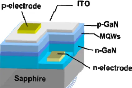
Benefit by the effort of such pioneers, the blue GaN-based light emitting diode (LED) is now successfully commercialized. The typical structure of a blue GaN-based LED is illustrated in figure 1.2. The layer of n-type GaN contains an excess of electrons, whereas the p-type layer is a region from which electrons have been removed (i.e., in which “holes” have been formed). If a forward bias is applied, electrons and holes can recombine, releasing energy in the transition layer in the form of light. The energy of the photon corresponds to the voltage bias in the transition region (the “bandgap”). Sapphire and silicon carbide are often used as substrates, which allow for large-area heteroepitaxial growth.
1-3 GaN Nano-structures
By the rapid developing of nano-structure fabrication techniques, we are now having the ability to fabricate GaN nano-structures. It is believed that nano-structures have totally different properties than the bulk material, so that attracted considerable interest for potential application to electronic and optoelectronic devices. By well control and shrink the structure sizes, we could not only save space and increase the capacity of a single chip, but also brings the benefits of quantum effects. The term we called “nano-structures” in this thesis means that one or more dimensions have been restricted to lengths in the order of the mean free path of charge carriers or excitons in the material. In general, the electron Fermi wavelength was far shorter than the size of bulk material so we could not observe the quantum confinement effect.
However, if we could condense one direction size smaller than the Fermi wavelength that the electron was forced to be freely moved in other two dimensions as shown in figure 1.3; such structure was called as a quantum well system. Furthermore, once there was a system with sizes smaller than the Fermi wavelength in two directions; we called it quantum wire. Of course, if we are able to reduce the structure size smaller than one wavelength in three directions, that was called as quantum dot. Actually, we had applied the concepts of nano-structure to modify and improve the device performance in many electronic or lighting devices like quantum wells in LED. It benefits to confine the electrons and holes in the quantum wells and improve the lighting efficiency effectively.
1-4 Overview of this thesis
This study has focused on fabricating a high efficiency GaN-based LED for next generation solid-state lighting by applying nanotechnology. The nanofabrication techniques and the device characteristics will be discussed in the thesis.
Since the overall efficiency of a LED could be viewed as a product of internal quantum efficiency (IQE) and extraction efficiency (ExE), we should put attention on both sides to meet the requirement of next-generation lighting devices. Therefore, the chapter 2 in this thesis will first introduce some nano-structures fabrication process and the characteristics including the comparison between nano-structure and bulk materials. Some simulation was performed to help understanding the inside information. Chapter 3 reports some high efficiency GaN-based LEDs employing nanotechnologies to improve the lighting efficiency. There are three different kinds of high efficiency LEDs demonstrated in this chapter. We first combined wafer bonding and laser lift-off (LLO) techniques to form a vertical-injected LEDs. Then, two methods to form high aspect ratio GaN nanorod by inductively coupled plasma (ICP) etching and ZnO nanorod by synthesizing in aqueous solution at room temperature. Both of them could help a lot to improve the ExE effectively. Third, by applying the nanorod fabrication technique shown in chapter 2, we form SiO2 nanorods on the sapphire surface and
regrowth GaN epi-layers on top of it. It not only improves the crystal quality but also benefits to ExE as well. The details of fabrication and device characteristics will be shown in this chapter.
For IQE issues, we had established an IQE measurement system by both photoluminescence (PL) and electroluminescence (EL) methods. The facilities and IQE measurement mechanism will be introduced in chapter 4. In chapter 5, we compared the IQE characteristics of two set of samples, LEDs on pattern sapphire substrate (PSS) and with
different quantum well thickness by PL and EL methods, respectively. It not only helps to realize the IQE but also the efficiency droop performance. Finally, chapter 6 is the summary of this thesis.
Reference:
1. S. Nakamura, M. Senoh, N. Isawa, and S. Nagahama, Japan Journal of Applied Physics 34, L797 (1995)
2. S. Nakamura, T. Mukai, and M. Senoh, Applied Physics Letter 64, 1687 (1994)
3. S. Nakamura, M. Senoh, S. Nagahama, N. Iwasa, T. Yamada, T. Matsushita, Y. Sugimoto, and H. Kiyoju, Applied Physics Letter 70, 868 (1997)
4. S. Nakamura, Science 281, 956 (1998)
5. Y. Arakawa, IEEE Journal of Selected Topics in Quantum Electronics 8, 823 (2002) 6. H. Morkoc, Nitride Semiconductors and Devices (Springer Verlag, Heidelberg), 1999 7. S. N. Mohammad, and H. Morkoc, Progress in Quantum Electronics 20, 361, (1996) 8. F. Bernardini and V. Fiorentini, Physica Status Solidi B 216, 391 (1999)
9. A. Hangleiter, J. S. Im, H. Kollmer, S. Heppel, J. Off, and F. Scholz, MRS Internet Journal of Nitride Semiconductor Research 3, 15 (1998)
10. H. Amano, N. Sawaki, I. Akasaki, and Y. Toyoda, Applied Physics Letter 48, 353 (1986) 11. S. Nakamura, Japan Journal of Applied Physics 30, L1705 (1991)
12. S. Nakamura, T. Mukai, M, Senoh, S. Nagahama, and N. Iwasa, Journal of Applied Physics 74, 3911 (1993)
13. H. Amano, N. Sawaki, I. Akasaki, and Y. Toyoda, Applied Physics Letter 48, 353 (1986) 14. H. Amano, N. Sawaki, I. Akasaki, and Y. Toyoda, Japan Journal of Applied Physics 28,
L2112 (1989)
Al Zn Si In GaN Lattice Constant : 3.189Å AlP GaAs Si ZnS GaP AlAs Z ZnnSSee ZZnnTTee InP GaSb AlSb InAs InSb CdTe Al2O3 (Sapphire)
Figure 1.1 The bandgap diagram of compound semiconductor materials.
3.0 3.5 4.0 4.5 5.0 5.5 6.0 6.5 0 1 2 3 4 5 6 7
?
Energy Bandgap (eV)
Figure 1.3 Schematic of quantum confined structures and Fermi wavelength
Quantum well
Quantum wire
Quantum dot
CHAPTER 2
Optical Properties and Strain Analysis of InGaN/GaN Nanorods
With the rapid development of nano-fabrication technology, fabrication and studies of nanorods in GaN-based semiconductors have attracted considerable interest for potential applications in electronic and optoelectronic devices due to the quantum confinement and the strain relaxation effect [1]. It is also reported that the InGaN/GaN nanorods can exhibit optical and electrical properties that are different from those in the bulk materials
GaN nanorods have been produced by various fabrication methods. In 1997, Han et al. first proposed synthesizing GaN nanorods by using carbon nanotubes as templates [2]. The dimension of the synthesized GaN nanorods could be up to 25 m in length and ranging from 4 to 50 m in diameter. However, preparing the carbon nanotube is rather complicated. The growth of single-crystal GaN nanorods by hybrid vapor-phase epitaxy [3] has been developed by Kim et al.A mask-free simple process by inductively coupled plasma-reactive ion etching (ICP-RIE) dry etching to fabricate GaN nanorods was proposed by Yu et al. [4]. The growth of GaN nanorods by using ferrocene as the catalyst, so-called vapor–liquid–solid (VLS) mechanism, was also demonstrated [5]. Fabrication of GaN nanorods by e-beam patterning and ICP etching was proposed by Chen et al. [6].
By the benefit of development of these nano-structure fabrication techniques, several GaN devices were then fabricated and the characteristics were studied. Johnson et. al demonstrated a single GaN nanowire lasing phenomenon in [7]. It is the first demonstration of single GaN nanowire laser. Han et. al. performed the photoconduction studies on GaN nanowire transistors under UV and polarized UV illumination in 2004 [8]. Besides, Kim et. al. demonstrated a high brightness LEDs by fabricating high quality, dislocation-free InGaN/GaN nanorods [9]. Finally, in 2006, Son et. al. demonstrated a UV photodetector by using a single GaN nanorod with p-n junction [10]. From these literatures, we could conclude that by the help of GaN nanostructure, we could obtain most of opto-electronic devices like laser, LED and photodetector from blue to UV region.
However, most of these GaN nano-structures are formed by epi-growth methods, which is not suitable for mass production in the present production. In addition, the typical structures prepared by these methods do not contain active layers, which limit the potential applications for optoelectronic devices. We developed a novel method to form GaN nanorod with InGaN/GaN multiple quantum wells (MQWs). The details of the nanostructure fabrication
and characteristics will be introduced in this chapter.
2-1 Fabrication Process
Generally, this nanorod fabrication process could be applied on any type of semiconductor material like Si, GaAs, GaN or sapphire substrate. In this chapter, we selected to form nanorod on the surface of GaN-based LED. The samples we used in this chapter were grown by metal–organic chemical vapor deposition (MOCVD) with a rotating-disk reactor on a c-plane sapphire (0001) substrate at a growth pressure of 200 mbar. The epitaxial structure consisted of a 30-nm-thick GaN nucleation layer, a 2-μm-thick unintentionally doped GaN buffer layer, a 2-μm-thick Si-doped n-GaN layer, an unintentionally doped InGaN/GaN MQW active region, and a 0.2-μm-thick Mg-doped p-GaN. The MQW active region consists of ten pairs of 3- and 7-nm-thick InGaN wells and GaN barriers.
Based on our previous experimental results, a thin metal film can be self-assembled into nano-scaled islands after rapid temperature annealing (RTA), and the metal islands can result in better distribution uniformity with a dielectric film deposited underneath the metal layer. Therefore, the nanorod formation process was started from depositing a thin dielectric film on top of the GaN LED surface as shown in figure 2.1. A 100-nm-thick SiO2 layer was first
deposited on the epi-surface of LEDs by plasma-enhanced chemical vapor deposition (PECVD). Then, we deposited a thin metal, Ni in this thesis, on top of SiO2 layer on the
purpose to form etching masks. We selected Ni metal because it could be obtained easily by E-gun evaporator. Besides, it has better etching selectivity to general semiconductor material like GaAs and GaN than other metals which enable us to form high aspect ratio nano-structures. A thin Ni metal layer was then deposited on the surface of the SiO2 layer
(figure 2.1(a)).and subsequently undergone the RTA process to form the self-assembly nanometer sized Ni clusters (figure 2.1(b)). The sample with Ni nanomasks on the surface were subsequently performed reactive ion etching (RIE) to remove SiO2 to transfer the
nanoscaled pattern into the SiO2 and ICP to form GaN nanorod structures (figure 2.1(d)). The
samples were then etched by the ICP-RIE system (SAMCO ICP-RIE 101iPH) operated at 13.56 MHz under a gas mixture of Cl2/Ar = 45/30 SCCM through individual electronic mass
flow controllers. The ICP source power, bias power, and the chamber pressure of the ICP-RIE system were set to 400W, 100 W, and 0.66 Pa, respectively. After the etching process, we use heated nitric acid to remove residual Ni masks and buffered oxide etchant (BOE) to remove the SiO2 on top of GaN nanorods (figure 2.1(e)). The details of each step will be introduced as
Effect of dielectric layer
As mentioned in previous paragraph, more uniform nano-masks could be obtained if an underneath dielectric layer was deposited first. The difference between these two cases, annealing with and without underneath dielectric layer was shown in figure 2.2. Figure 2.2 is the scanning electron microscope (SEM) images. Figure 2.2(a) shows the annealing results on top of dielectric layer and (b) shows that on GaN surface. A discrete Ni nano-cluster array could be observed at the surface. In this figure, the diameter is ranging from about 90 to 140 nm. On the other side, the annealed Ni nano-clusters on bare LED surface show a non-uniform pattern in the diameters and behaved a sheet-like result instead of dot-like structure. This difference could be explained by the strain effect. The room temperature lattice constant of Ni was about 0.352 nm and that of the corresponding crystalline GaN surface to be 0.318 nm in a direction and 0.518 nm in c direction. This gives the room temperature strains were εa(GaN/Ni)= 10% and εc(GaN/Ni)=-32%. However, the dielectric SiO2 has a lattice
constant to be 0.49 nm in the a direction and 0.54 nm in the c direction gives the room temperature strains as εa(SiO2/Ni)= -28% and εc(Si3N4/Ni) =-35% respectively. This means that the
deposition of Ni on SiO2 bears a higher tensile strain in both a and c directions which results
in a smaller and more uniform nano-cluster array in the surface [11]. Besides, by depositing a dielectric underneath layer like SiO2 or Si3H4, we could sustain the large strain between these
two layers which means we could ignore possible strain variation resulted from substrate. That means we are able to form these kind of nano-structure at any material surface as long as there is no temperature issues.
Effect of Ni thickness
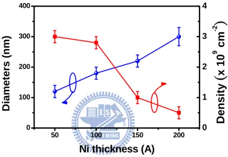
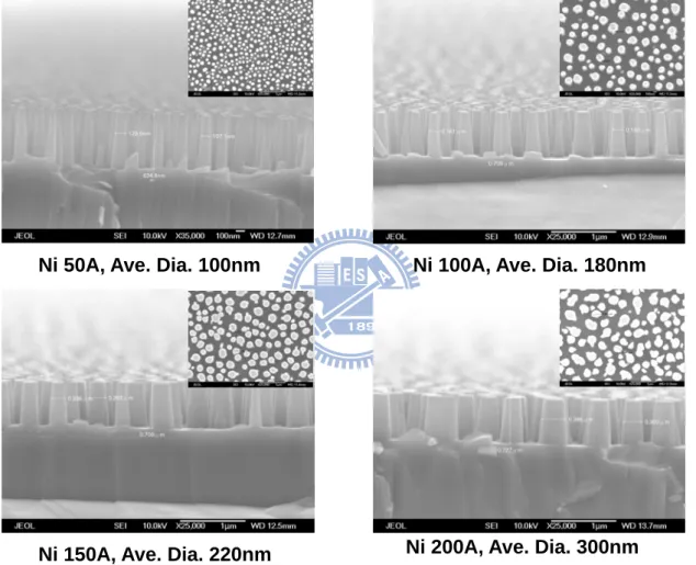
Regarding to the geometry and density of the formed Ni nano-clusters, we conclude two main factors, the Ni layer thickness and the RTA temperature. In order to find out the effect of different thickness, we varied the deposited Ni thickness from 50 to 200 Å on the surface of 100 nm SiO2 layer on top of GaN-based LED. The RTA temperature and maintain time was
fixed at 850 oC with a ramp of 40 oC/sec and 60 sec to form nano-clusters. The diameter and density of the formed nano-clusters were shown in figure 2.3. We could find that the average diameter was 120 ± 20, 180 ± 20, 220 ± 20, and 300 ± 30 nm while the deposited Ni thickness increasing from 50 to 200 Å. On the other side, the density decrease from 3 to 0.5 x 109 cm-2 with the increasing thickness. We could conclude that the diameter was proportional to the Ni thickness but the density has an opposite trend.
Effect of RTA temperature
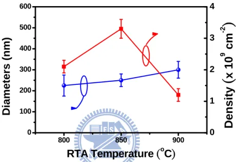
Besides the Ni thickness, RTA temperature is another very important factor to determine the geometry of formed nano-clusters. In this case, we fixed the thickness of Ni layer and varying the RTA temperature from 800 to 900 oC with a constant ramping speed of 50 oC/sec lasting for 60 sec, and the results were shown in figure 2.4. As the RTA temperature increased from 800 to 900 oC, the diameter increased steadily from about 210 ± 20 to 300 ± 20 nm. Here we could find out a maximum in density at the RTA temperature of about 850 oC which implies a shortest spacing between each cluster at the surface. From observation of these two factors, it is easier for Ni to migrate and results in a smaller cluster size and higher distribution density. That also indicates that we could modify the diameter and density by well control the initial Ni thickness and RTA temperature.
2-2 Height-dependent Antireflection Properties
Recently, the interests in nano-scaled antireflection (AR) textures have been extended to disordered structures, where the fabrication cost is significantly reduced without the requirement of the electron beam lithography. Moreover, a variety of materials, including Si, GaAs, and glass [12], are available for the applications, offering versatile device possibilities. While several studies have been made on the reflectivity characterizations of disordered nanostructures [13-15], few reports have discussed the correlation between the reflective characteristics and the structural properties, such as geometric shapes, dimensions, and densities. Calculations on the reflectivities of nanostructures are also a challenge due to the nature of disorder, hindering further progress in device design and analysis. In this work, we have fabricated GaN nanorod structures with three different heights: 300, 550, and 720 nm. Since GaN is a wide bandgap material [16], the observed AR characteristics can be correlated with the structural properties. The fabrication process and AR characteristics of GaN nanorod with different height will be discussed and an algorithm based on a rigorous coupled-wave analysis (RCWA) method is also developed in this section.
Sample preparation
Based on previous GaN nanorod fabrication experience, in this section, we fabricated three different set of GaN nanorods with heights of h=300, 550 and 720 nm, corresponding to the etching times of 60, 90 and 120 sec, respectively. Figures 2.5(a) to (c) show the cross-sectional views of the fabricated samples. The respective etching rates were
approximately 5, 6.11, and 6 nm/sec, indicating a slower etching rate at the beginning period due to the unapparent initial bombardment efficiency. However, the etching rate was decreased again at the etching time of 120 sec because, as shown in figure 2.5(b), the lateral etching of nanorod became noticeable, limiting the etch depth. A deeper nanopillar structure could be achieved if the flow rate of the etching gas (Cl2) was reduced along with an increase
in ICP power. It is found that the flow rate of Cl2 and ICP power are critical in controlling the
shape of nanorod.
Reflectivity measurement
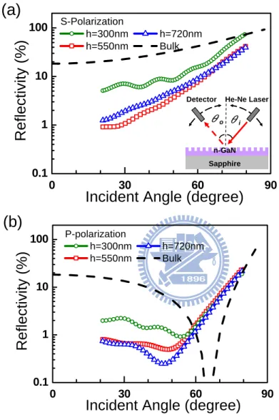
The reflectivity of the n-GaN nanopillars was characterized as a function of the incident angle for both s- and p- polarizations, using a linearly polarized He-Ne laser at λ= 632.8 nm. The incident power was set to 3 mW with a spot size of ~1mm. As shown in the inset of figure 2.6, light struck on the sample at an incident angle θi, with respect to the surface normal,
while the detector on the other side received the reflected light at the same angle, θo=θi. Both
angles were varied from 20˚ to 80˚. The system was calibrated with a silicon substrate before measurements. For reflectivity spectroscopy, the incident light was obtained from a monochromator using a xenon lamp with wavelengths ranging from 300 to 1800 nm.
The measured angle-dependent reflectivities for GaN nanorods of different heights are shown in figure 2.6(a) for s-polarization and (b) for p-polarization. The calculated reflectivities of bulk GaN (n=2.5) for both polarizations are also plotted for reference. As shown in figure 2.6, the angular reflectivities in GaN nanorod structures have been drastically reduced from those of bulk. As shown in figure 2.6(a), the reflectivities of s-polarization for h=550 and 720nm are nearly identical, showing excellent AR characteristics (<3%) up to an incident angle of 50o. The reflectivities for h=330nm are relatively high and the interference from air/GaN and GaN/sapphire interfaces can also be observed. The interference characteristics completely vanish for h=550 and 720 nm, since the scattering on the nanorod surfaces give rise to phase randomization. As shown in figure 2.6(b), the measured reflectivities for three different heights are lower than 3% up to an incident angle of 60˚ for p-polarization. It is worth noting that the reflectivities of nanorod decrease as the incident angle increases before Brewster’s angle, similar to those of bulk. Although Brewster’s angle becomes indiscernible in nanorod structures, minimal reflectivities occur at incident angles of 53.5o, 48.8o, and 46.4o for h=300, 550, and 720 nm, respectively, showing a linear correlation between the pillar height and the incident angle of the minimal reflectivity. This characteristic
can also be observed in the reflectivity ratio of polarizations, that is, the ratio of the reflectivity of the s-polarization to that of the p-polarization, denoted as Is/Ip. As shown in Fig.
3, the bulk GaN exhibits a peak of Is/Ip >104 at Brewster’s angle of 63.5o, while Is/Ip drops
significantly to <20 for all nanorod structures. As the height of the nanorod increases, the peak of Is/Ip shifts towards a smaller incident angle. Figure 2.7 suggests that the reflectivities
become polarization-insensitive even in a shallow nanostructured surface. It is also worth noting that the ratio Is/Ip is enhanced at small incident angles, since the spatial symmetry of
bulk at the normal incidence is altered by the nanostructures. Similar results have been observed in GaN nano-wires on sapphire with different coverage ratios [17].
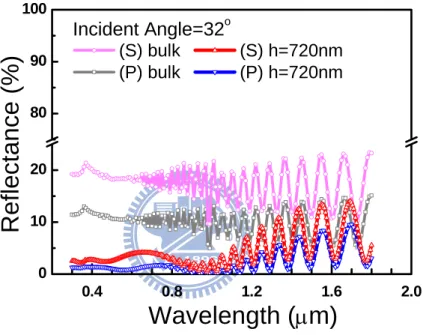
The reflectivity spectroscopy with light incident at an angle of 32o is shown in figure 2.8. Bulk GaN exhibits reflectivities of ~23% for s-polarization and ~13% for p-polarization in the wavelength range between 300 nm and 1800 nm, while the GaN nanopillars of h=720 nm show reflectivities <5% in the 300-1200 nm wavelength range, and <10% in λ=1200-1800 nm for both polarizations.
Reflectivity simulation
The measured data for GaN nanorods with a height of 720nm shows superior angular and spectral antireflection. However, the reflective characteristics of nanorods of different heights do not show significant differentiation that could determine the best fabrication parameters. Although the random variation of pillar widths and positions can not be accurately controlled, it is of great interest to understand the structural properties, such as the density, geometric shapes, and dimensions that contribute to superior AR characteristics. A thorough theoretical study can facilitate the design and fabrication of nano-structured AR surfaces. Therefore, a theoretical model based on a RCWA method is developed to investigate the dependence of the AR characteristics on the structural properties of nanorods.
The RCWA method is often employed to solve the diffraction and transmission efficiency of optical diffractive elements, where the reflectivity is obtained as a sum of the reflected diffraction efficiencies of different diffraction orders. In order to minimize the calculation errors arising from periodic boundary conditions in disordered structures, a unit-cell is defined with dimensions at least an order of magnitude larger than the incident wavelength. The size of unit cell and randomness of nanorod positions have also been studied to ensure convergence. Calculations show that a refractive-index gradient between air (n=1) and bulk GaN (n=2.5) is the key element to significantly reduce the reflection, since the
incident light can hardly experience the changes in dielectric environments. Therefore, the shape of nanorods, which determines the refractive-index gradient, is desired to be a cone-like structure. The periodic SWS with shapes of pyramids are nearly ideal AR structures, since the nano-pyramids provide a linear gradient of the refractive indices between air and the silicon substrate [18]. In order to apply the design concept to disordered structures, we can define the fill factor as the ratio between the areas covered by nanorod with respect to a unit cell. It is desirable that the fill factor at the base of the nanorods approaches one while that at the top approaches zero.
We first investigate the origins of the omnidirectional antireflection by fitting the measured data. Since both the density and the base/top diameters of the nanorods determine the fill factors, the random variation in the pillar width is neglected for simulation. Moreover, a linear refractive-index gradient is assumed. Figure 2.9(a) shows the refractive-index profile of a unit cell, which consists of 7x7 random nanorod s with a height of 720nm. The unit cell has an area of ~1.6 μm2, corresponding to a density of ~3x109cm-2. The top/bottom diameters
of the pillars with h=300nm, 550nm, and 720nm are chosen to be 140/170, 100/180, and 80/190 nm, respectively. The calculated reflectivities of random nanorod s are plotted as a function of the incident angle in figure 2.9(a) for (b) h=300nm, (c) h=550nm, and (d) h=720nm. Since the latter two share a similar refractive index gradient and fill factors in simulation, we attribute the omnidirectional antireflection to the tapered refractive-index profile due to the slight lateral etching of the nanopillars, as seen in figure 2.5(c) for h=550nm and figure 2.5(d) for h=720nm. On the other hand, the AR properties for h=300nm are limited by the etch depth and the pillar profile.
2-3 Size-dependent Optical Characteristics and Strain Relaxation Analysis
In GaN material system, there inherently exists large internal strain in GaN material and the MQWs and QCSE effect leading to the wave-function separation in electrons and holes. Since it has been known that fabricating nano-structures could modify and reduce the existing strain, it is of great interest to investigate the degree of strain relaxation by different GaN nanorod sizes. In this section, we fabricated four different sizes of GaN nanorods by depositing different thickness of Ni layer ranging from 50, 100, 150 to 200 Å. With fixed RTA temperature of 850 oC and RIE and ICP etching process to define SiO2 and transfer it
into GaN layer, we could get different diameter and density of nanorod arrays. From observation of SEM images from these fours samples with different initial Ni thickness as shown in figure 2.10, we could find the diameter of formed nanorods were 120 ± 20, 180 ± 20,
220 ± 20, and 300 ± 30 nm and the density decreased as thicker Ni thickness.
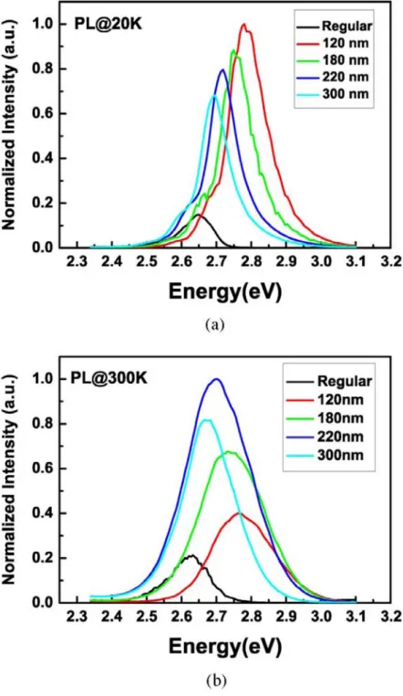
Optical properties
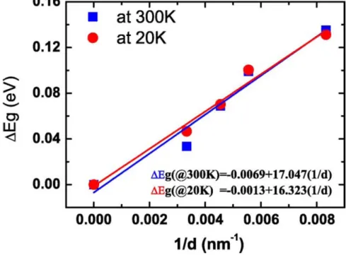
Figure 2.10 (a) and (b) shows the measured PL from a regular LED and nanorod LEDs with various average diameters at low temperature 20K and room temperature, respectively. The pumping powers for all measurements are 15 mW at a laser spot size of 200 μm. As shown in figure 2.10(a), as the averaged rod diameter becomes smaller, the emission peak shows a clear blue shift. The PL intensity is strongest for LEDs with the smallest averaged diameter, 120 nm. The intensity decreases as the diameter becomes larger. However, the PL characteristics at room temperature are slightly different from those at the low temperature 20 K. First, the emission peak still has a clear blue shift as the diameter becomes smaller. Second, the PL intensity is strongest for LEDs with an averaged diameter of 220 nm. PL intensities are deteriorated at room temperature for nanorod LEDs of 120 and 180 nm. The PL intensity of the regular LED is much weaker than nanorod LEDs due to a stronger QCSE and lower light extraction efficiency. Figure 2.11 shows the peak energy shift versus the rod diameters. The PL peak position of the regular LED is also plotted as the reference point. We can find that the fitted slopes at room temperature and 20 K are around 17.047 and 16.323 eV·nm, respectively.
The changes in PL intensity could be due to the absorption of excitation, the emission volume, light extraction efficiency, and defect densities of the nanorod LEDs. Therefore, it is hard to quantitatively analyze the size-dependent characteristics of the PL intensity and we will discuss qualitatively later. On the other hand, the blue shift of the spectrum is large (>100 meV) and cannot be simply explained by the band-filling effect or the carrier screening of QCSE. In particular, the power density of PL is not strong enough to induce a very high carrier density in the MQWs. The other possibility is the strain relaxation of the QW [18]. For InGaN/GaN, QW structures grown along c-axis, there exists a strong strain-induced piezoelectric polarization field inside the device. This will contribute to the band bending and red shift of spectrum, known as the QCSE. For the QW structure at the edge of nanorod surface, the lateral confinement of the QW is weak such that the relaxation of the InGaN QW layer is possible. The relaxed strain reduces the piezoelectric field inside theQWso that the spectrum shows a blue shift of the emission wavelength. This blue shift should be observed for low power, high-power, low-temperature, and room-temperature PL measurements.
As mentioned earlier, the PL intensity of the nanorod with the smallest diameters is the strongest at low temperature. However, at room temperature, the PL intensity maximum
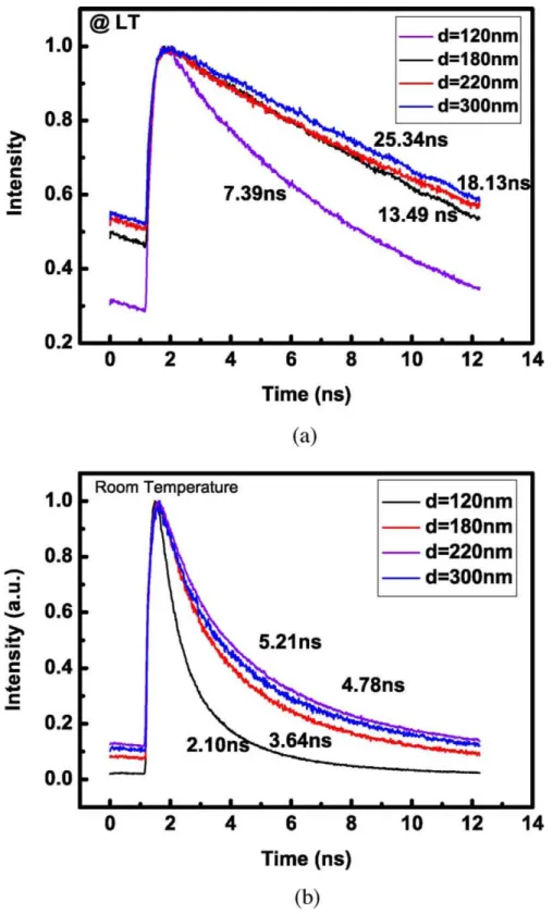
occurs for nanorod LEDs with an average diameter of 220 nm. The effects of extraction and absorption may be neglected since they were measured from the same samples only at different temperatures. It is possible that the defect density contributes to the decease of the PL intensity. Therefore, we conduct the time-resolved photoluminescence (TRPL) for both cases. Figure 2.13(a) and (b) shows the measured TRPL at low temperature 20 K and room temperature, respectively. As shown in figure 2.13(a), the fitted decay times are 25.34, 18.13, 13.49, and 7.39 ns for nanorod diameters of 300, 220, 180, and 120 nm, respectively. The nanorod LEDs with the diameter of 120 nm have the smallest decay time. If the carrier decaying process is dominated by radiative recombination, the smallest diameter nanorod has the best efficiency. This can be also observed with the PL spectrum intensity, as shown in Figure 2.11(a). However, at room temperature, we can find that the nanorod LEDs with the diameter of 220 nm have the strongest emission intensity. However, as shown in figure 2.13(b), the TRPL shows that the decay time of 120 nm nanorod has the smallest decay time. It is well-known that the PL decay lifetime is determined by both the radiative and nonradiative processes. If the radiative lifetime dominates, the emission intensity should be strongest for the smallest nanorod size due to the smallest decay time. However, the intensity of nanorod LEDs with a diameter of 120 nm exhibits an opposing behavior, as shown in figure 2.11(b). Hence, we conclude that the nonradiative decay process dominates and reduces the emission intensities at room temperature. The nanorod LEDs with a diameter size smaller than 180 nm may have a large defect density. Although the nanorod LEDs with a small averaged diameter can increase the radiative recombination rate, the increased nonradiative recombination rate cancels the effect of radiative rate enhancement and limits the internal quantum efficiency.
VFF simulation
In order to confirm the observed wavelength blue shift, we first apply the valence force field (VFF) model [19]. Once the atoms’ positions are known, calculating the strain tensor distribution is straightforward. To maintain the symmetry in a wurtzite structure, free-standing, cylindrical-shaped GaN nanorods consisting of ten-pair In0.2Ga0.8N MQWs are
defined with various diameters ranging from 120 to 300 nm. The nanorod has a fixed boundary condition at the bottom and free boundary conditions on other sides. Figure 2.14 shows the calculated strain distribution for the nanorod with a diameter equal to 120 nm. Figure 2.14(a)–(c) shows the strain tensor εxx, εyy, and εzz of the cross section of x − z plane at
(center) of strain tensor. Both strain tensors show considerable relaxations on the outer shell of the nanorod, and as-grown-like strain distributions in the center of the nanorod. As shown in figure 2.14(a), the strain relaxation of εxx occurs at a distance of 20 nm from the edge of the nanorod. At r = 58 nm, where the change of strain from the nanorod center is most significant, there exist substantial strain variations on the QW/barrier interfaces and a slight tensile strain of εxx in the barriers. There is also a slight strain relaxation of _yy due to the circular shape of the rod. We also observe a vertical distribution of εzz in the Z-direction, mainly arising from the stacking of MQWs.
Figure 2.15(a)–(d) shows the strain tensors εxx for nanorod diameters equal to 120, 180,
220, and 300 nm, respectively. As shown in figure 2.15, the major strain relaxation region is limited to 20 nm from the edge, regardless of the rod diameters. Therefore, the ratio of strain-relaxed MQW region to the strained region size becomes larger as the diameter decreases. With the calculated strain information, it is possible to calculate the emission spectra of nanorod LEDs with different sizes. Both in-plane and vertical strain tensors contribute to the polarization field and can be calculated by the following equation:
Pez =e31(εxx+εyy)+e33εzz (2-1)
where e31 and e33 are the piezoelectric coefficients and can be found in Ambacher et al. [20]. Based on the calculated strain, as shown in figure 2.14, and the induced polarization harge calculated by ( , , ) ( , , ) ( , , ) ez ez pz P x y z dz P x y z x y z dz ρ = + − (2-2)
The calculated results are subsequently inserted into the self-consistent Poisson, Schr¨odinger, and drift-diffusion solver to calculate the band structure of the MQWs. The parameters needed for the band structure calculation can be found in Ambacher et al. [20].
Figure 2.16 shows the calculated band structures of the ten-pair MQW structure for different strain conditions: (a) at the center and (b) at the edge of the nanorod with a diameter of 120 nm. The polarization charge density induced by strain is taken into account as a function of the depth and the spontaneous polarization. As shown in Fig. 7, the band bending at the center of the nanorod is the strongest while the band bending at the edge is the weakest at r = 58 nm, where the strain relaxation reaches the maximum. In order to compare the PL intensity and compare the energy shift of the emission peak at different regions, we use the following equation to calculate the emission intensity and the energy shift.
2 2 2 , , 2 3 2 2 2 , 0 0 ( ) 2 1 ( ) k p exp( ) (2 ) 2 2 i j e h r spon i j i j E e n R d d a f f m c ω ω ω ε π πσ σ − − =
∫
∑
∫
i × (2-3)where Ei,j is the averaged energy separation between the electron state i and hole state j, nr is
the refractive index, and σ is the inhomogeneous broadening factor. fe(k) and fh(k) are the Fermi–Dirac distribution of electrons and holes, respectively. |a·pi,j |2 is the momentum
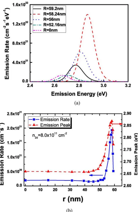
matrix element between the electron state, i, and the hole state, j. The calculated results are shown in figure 2.17. Figure 2.17(a) shows the calculated emission spectra of the MQW structure at different regions of the nanorod structure with a diameter of 120 nm and under an injected electron density of 8×1011 cm−2 (n3d~2.7×1018 cm−3). The average hole density is
around 7×1012 cm−2, which is much higher than electron density due to the heavier effective mass and smaller diffusion length so that more holes stay inside the QW after electron–hole pairs are generated. As shown in figure 2.17 (a), the emission intensity near the edge is the strongest. For r<45 nm, the emission strength does not change much, and this can be explained by the insignificant strain variation from the center, as shown in figure 2.14. Moreover, figure 2.17(b) shows the calculated emission peak shift and emission rates as a function of the radius of the cylindrical nanorod under an injected electron density of 8 × 10¹¹
cm−2. The maximum emission peak shift occurs at r=58 nm where 200 meV blue shift is
achieved, compared to the emission from center of the nanorod. At r=60 nm, the strain relaxation is not the maximum at the surface so that the energy shift maximum does not occur here. The emission rate reaches the maximum at edge and decreases rapidly from r=60 nm to r=45 nm. The emission rates are almost constants for r<45 nm, where the electron–hole wavefunction overlap does not change too much here. Since the center of MQWs are still suffered from the strain with its magnitude comparable to that of the as-grown planar structure, the PL from the center of the nanorod contributes to the red-edge emission, which is partially overlapped with the PL from the strained region. Therefore, we believe that the majority of the nanorod PL blue shift originates from the strain relaxed region, within a distance of ∼15 nm near the edge of the nanorod, as shown in figure 2.17(b). Moreover, the variation of strain tensors in the relaxation region results in a spatially varied polarization field, leading to a broadened emission spectrum.
Reference:
1 C. H. Chiu, M. H. Lo, T. C. Lu, P. Yu, H. W. Huang, H. C. Kuo, and S. C. Wang, IEEE Journal of Lightwave Technology 26, 1445 (2008).
2 W. Q. Han, S. S. Fan, Q. Q. Li, and Y. D. Hu, Science 277, 1287 (1997).
3 H. M. Kim, D. S. Kim, T. W. Kang, Y. H. Cho, and K. S. Chung, Applied Physics Letter
81 2193, (2002).
4 C. C. Yu, C. F. Chu, J. Y. Tsai, H. W. Huang, T. H. Hsueh, C. F. Lin, and S. C. Wang, Japan Journal of Applied Physics 41, L910 (2002).
5 W. Q. Han and A. Zettl, Applied Physics Letter 80, 303 (2002).
6 H. S. Chen, D. M. Yeh, Y. C. Lu, C. Y. Chen, C. F. Huang, T. Y. Tang, C. C. Yang, C. S.Wu, and C. D. Chen, Nanotechnology 17, 1454 (2006).
7 J. C. Johnson, H. J. Choi, K. P. Knutsen, R. D. Schaller, P. D. Yang, and R. J. Saykally, Nature Material 1 106 (2002).
8 S. Han, W. Jin, D. H. Zhang, T. Tang, C. Li, X. L. Liu, Z. Q. Liu, B. Lei, and C. W. Zhou, Chemical Physics Letter 389, 176 (2004).
9 H. M. Kim, Y. H. Cho, H. Lee, S. I. Kim, S. R. Ryu, D. Y. Kim, T.W. Kang, andK. S. Chung, Nano Letter 4 1059 (2004).
10 M. S. Son, S. I. Im, Y. S. Park, C. M. Park, T.W. Kang, and K. H. Yoo, Material Science and Engineering C-Biomimetic and Supramolecular System 26, 886 (2006).
11 J. D. Carey, L. L. Ong and S. R. P. Silva, Nanotechnology 14, 1223 (2003).
12 D. S. Hobbs, B. D. MacLeod, and J. R. Riccobono, Proc. of SPIE 6545 65450Y-1-14, (2007)
13 G. R. Lin, Y. C. Chang, E. S. Liu, H. C. Kuo, and H. S. Lin, Applied Physics Letter 90, 181923 (2007).
14 Y. Kanamori, K.-I. Kobayashi, H. Yugami, K. Hane, Japan Journal of Applied Physics 42, 4020 (2003)
15 Y. Zhao, J. Wang and G. Mao, Optics Letter 30, 1885 (2005)
16 S. Nakamura, M. Senoh, S. Nagahama, N. Iwasa, T. Yamada , T. Matsushita, H. Kiyoku, and Y. Sugimoto, Japan Journal of Applied Physics 35, L74 (1996).
17 Y. Du. S. Han, W. Jin, C. Zhou, and A. F. J. Levi, Applied Physics Letter 83, 996-998 (2003)
18 P. Yu, C. H. Chiu, Y.-R.Wu, H. H.Yen, J. R. Chen, C. C. Kao, H.-W. Yang, H. C. Kuo, T. C. Lu, W. Y. Yeh, and S. C. Wang, Applied Physics Letter 93, 081110 (2008).
19 Y.-R. Wu, M. Singh, and J. Singh, Journal of Applied. Physics 94, 5826 (2003).
20 O. Ambacher, J. Majewski, C. Miskys, A. Link, M. Hermann, M. Eickhoff, M. Stuzmann, F. Bernardini,V. Fiorentini,V. Tilak,B. Schaff, and L. F. Eastman, Condens. Material 14, 3399 (2002).
Figure 2.1 Schematic of GaN nanorod fabrication process
RTA
RIE
Ni 10 nm
SiO
2100 nm p-GaN
MQWs
n-GaN
Sapphire
Ni clusters
ICP
Masks remove
(a) (b) (c) (d) (e)(a)
(b)
Figure 2.2 SEM images of nano-clusters formed on the surface of (a) SiO2 layer and (b) GaN material.
50 100 150 200 0 100 200 300 400 0 1 2 3 4
Density
(
x 10
9cm
-2)
Diameters (nm)
Ni thickness (A)
Figure 2.3 The relationship of diameters and densities of the formed Ni nano-clusters versus the Ni thickness.
800 850 900 0 100 200 300 400 500 600 0 1 2 3 4
Density
(
x 10
9cm
-2)
Diameters (nm)
RTA Temperature
(
oC
)
Figure 2.4 The relationship of diameters and densities of the formed Ni nano-clusters versus the RTA temperature.
Figure 2.5 Cross-sectional views of the FESEM graphs for fabricated nanorod structures with heights of (a) 300 nm, (b) 550 nm, and (c) 720 nm.
(a)
(b)
0 30 60 90 0.1 1 10 100
Reflectivity (%
)
Incident Angle (degree)
S-Polarization h=300nm h=720nm h=550nm Bulk(a)
Sapphire n-GaN θi θoDetector He-Ne Laser
0 30 60 90 0.1 1 10 100
R
eflectivity (%
)
Incident Angle (degree)
P-polarizationh=300nm h=720nm h=550nm Bulk
(b)
Figure 2.6 Measured reflectivities of GaN nanorods with three different heights: h=350nm, 550nm, and 720nm, for (a) s-polarization and (b) p-polarization. The inset shows a schematic of the measurement setup.
20 40 60 80 1 10 100 1000 10000
Ref
lect
vity Rat
io, I
s
/I
p
Incident Angle
(
degree
)
h=720nm
h=550nm
h=300nm
Bulk GaN
Figure 2.7 The reflectivity ratio of polarizations, Is/Ip for bulk GaN, and nanorods of h=300, 550, and 720 nm is plotted as a function the incident angle. The reflectivities of nanorod structures are polarization-insensitive compared to those of bulk.
0.4 0.8 1.2 1.6 2.0 0 10 20 80 90 100
Reflectance (%)
Wavelength (
μ
m)
(S) bulk (S) h=720nm (P) bulk (P) h=720nm Incident Angle=32oFigure 2.8 The reflectivity spectroscopy for bulk GaN and the nanopillars with a height of 720 nm at an incident angle of 32o.