國 立 交 通 大 學
資訊科學與工程研究所
碩 士 論 文
多輸入多輸出鎖相迴路軟體化之研究
The Study of MIMO Software-defined Phase-locked Loop
研 究 生:黃則斌
指導教授:許騰尹 教授
多 輸 入 多 輸 出 鎖 相 迴 路 軟 體 化 之 研 究
The Study of MIMO Software-defined Phase-locked Loop
研 究 生:黃則斌 Student:Ze-Bin Huang
指導教授:許騰尹 Advisor:Terng-Yin Hsu
國 立 交 通 大 學
資 訊 科 學 與 工 程 研 究 所
碩 士 論 文
A ThesisSubmitted to Institute of Computer Science and Engineering College of Computer Science
National Chiao Tung University in partial Fulfillment of the Requirements
for the Degree of Master
in
Computer Science June 2009
Hsinchu, Taiwan, Republic of China
摘要
本 篇 論 文 提 出 了 可 軟 體 控 制 及 開 發 的 多 輸 入 多 輸 出 軟 體 鎖 相 迴 路 平 台 (MIMO-SDPLL)。此平台並結合了數個矽智財包括 CPU 及鎖相迴路的相關模組。CPU 的引 進,為平台提供有彈性的軟體控制及運算。在輸出規格需要大幅更動時,以變更軟體的 方式即能符合所需要的規格。本論文所提出的軟體鎖定演算法能達到高解析度鎖定的狀 態並且以軟體的方式進行開發。多重時脈輸入能用軟體排程的方式進行處理。硬體方 面,以 2 對 2 的架構進行作。所有的矽智財實作於 UMC 90nm 的製程上。
Abstract
A software controllable and programmable MIMO software-defined phase-locked loop (MIMO-SDPLL) platform is presented in this paper. This platform combine several silicon IPs including CPU and PLL modules. CPU is introduced to provide flexible software controllability and computing power. When the specification needs substantially modify, replace the software at platform can fit the new specification. The proposed software tracking algorithm can reach high-resolution phase-locked and development by software. Multi-clock can be handled with software scheduling. In hardware, 2x2 MIMO-SDPLL architecture is implemented in this work. All IP cores implement at UMC 90nm process.
誌謝
能完成這篇論文,首先要感謝我的指導教授許騰尹老師。老師有耐心的導引我論文 的研究方向,並適時的讓我獨立思考,培養解決問題的能力。在實驗室的資源提供上也 相當充足,老師會盡力爭取實驗室所需的工具。亦特別感謝 ISIP Lab 的成員及 PLL group。大家地無私互相分享知識及經驗才能順利完成這篇論文。最後感謝交通大學提 供相當良好的研究環境及家人的支持與鼓勵,讓我的碩士學業能順利的完成。 黃則斌 謹誌 民國九十八年八月十七日Table of Contents
摘要...i
Abstract ...ii
誌謝...iii
Table of Contents ...iv
List of Figures ...vi
List of Tables ...vii
Chapter 1 Introduction ...1
1.1. Thesis Motivation ...1
1.2. Thesis Contribution ...1
1.3. Thesis Organization ...2
Chapter 2 Overview of MIMO-SDPLL...3
2.1. Base Concept ...3 2.2. Silicon IP Selection...4 2.2.1. CPU ...4 2.2.2. BUS ...5 2.2.3. PLL ...5 2.3. Software...6 2.4. MIMO-SDPLL ...6
2.5. Architecture Simulator and IP Model ...8
2.5.1. Architecture simulator ...8
2.5.2. PLL IP Model ...8
Chapter 3 Tracking Algorithm ...10
3.1. Basic Concept of Frequency Search...10
3.2. Basic Concept of Phase Tracking ...12
3.3. The Challenge of Tracking Algorithm...13
3.4. The Proposed Tracking Algorithm ...16
3.4.1. TDC and DCO relation mapping...17
3.4.2. Frequency search algorithm ...18
3.4.3. Coarse tracking algorithm ...19
3.4.4. Fine tracking algorithm ...20
3.5. Scheduling of MIMO-SDPLL ...24
Chapter 4 Implementation and Simulation Result...26
4.1. Hardware ...26
4.1.1. Memory Map ...28
4.1.2. CPU ...29
4.1.5. Semi-asynchronous clock access (SACA) module ...33
4.2. Software...34
4.2.1. Software programming...34
4.2.2. Memory map I/O control...35
4.3. Simulation Result ...35
Chapter 5 Conclusion and Future Work ...38
List of Figures
Fig.1. Basic block diagram of ADPLL...4
Fig.2. OpenRISC OR1200 overview...5
Fig.3. Software flow of MIMO-SDPLL...6
Fig.4. MIMO-SDPLL architecture ...7
Fig.3.1. Binary search concept ... 11
Fig.3.2 The structure of time-to-digital converter (TDC) ...12
Fig.3.3 The simple phase tracking algorithm ...12
Fig.3.4. TDC-based phase tracking algorithm...13
Fig.3.5. Define of waveform expression. ...14
Fig.3.6. Setting new DCO control word...15
Fig.3.7. The close loop of tracking problem...16
Fig.3.8 The algorithm flow...17
Fig.3.9. TDC value and control word mapping...18
Fig.3.10 The estimation of reference clock ...19
Fig.3.11. Waveform of coarse tracking algorithm ...20
Fig.3.12. Different start position of coarse tracking algorithm ...20
Fig.3.13 The problem of fine tracking...21
Fig.3.15. The example of fine tracking algorithm...23
Fig.3.16. The working flow of fine tracking algorithm...24
Fig.3.16. The scheduling of 2×2 MIMO-SDPLL...25
Fig.4.1. 2×2 MIMO-SDPLL architecture...27
Fig.4.2 Memory map of 2×2 MIMO-SDPLL...29
Fig.4.3 WISHBONE read / write timing graph ...31
Fig.4.5. An example of SACA...33
Fig 4.6. The modified SACA block diagram...34
Fig.4.7. The waveforms of simulation result...37
List of Tables
Table 1 Hardware specification ...28 Table 2 Software environment...35 Table 3 Simulation setting ...36
Chapter 1
Introduction
1.1. Thesis Motivation
There are some types of PLLs, such as analog PLL, digital PLL (DPLL), and all-digital PLL (ADPLL) [1] [2]. All-digital approach brings portability and short design cycle in PLL design. However, designer often need redesign complexity circuit when algorithm or control strategy changed. With standard IC process, redesign also needs some time to run simulation, synthesis, layout and verification. It’s still longer than software development. So a new type of PLL with flexibility of reprogramming and reusability of silicon IPs called software-defined phase-locked loop (SDPLL) [3] is proposed.
The proposed SDPLL use a CPU to link all IPs via shared bus architecture. These IPs include those IPs modular from PLL and the other IPs are memory, flash and I/O device. With the flexibility of CPU, designer can implement tracking algorithm or controlling strategy in high level language like C language. Moreover, the calculation power of CPU let SDPLL can integrate more PLL IPs. Multiple clock output makes more possible combination of application. Here, this architecture with multi-input and multi-output is called MIMO software-defined phase-locked loop (MIMO-SDPLL). How to integrate these IPs into MIMO-SDPLL become a challenge.
1.2. Thesis Contribution
The proposed MIMO-SDPLL achieve high-resolution phase-locked with software control. Multi-clock can be handled by CPU with scheduling. When the specification needs substantially modify, replace the software at platform can fit the new specification.
1.3. Thesis Organization
Section 2 shows the overview of MIMO-SDPLL from hardware and software. Section 3 illustrates the proposed tracking algorithm. Section 4 is the implementation architecture includes software and hardware. Section 5 presents the simulation result of 2×2 MIMO-SDPLL and future work.
Chapter 2
Overview of MIMO-SDPLL
In this work, the proposed MIMO-SDPLL has feature of software controllability and programmability which integrates CPU with silicon IPs. These silicon IPs include PLL IPs. Here MIMO-SDPLL is discussed from some parts.
2.1.
Base Concept
In section 1, there are three type of PLL. For SoC implement issue, all-digital approach is suitable and easier. So ADPLL is chosen as basic PLL IPs.
Fig.1 shows conventional ADPLL block diagram. Include phase frequency detector (PFD), time to digital converter (TDC), digital control oscillator (DCO) and frequency divider (Divider N). ADPLL can generate frequency-locked and phase-locked clock output when input reference clock. After power on, PFD detect frequency or phase error between reference clock and divided-by-N clock. TDC converter error pulse received from PFD into digital data. If TDC output and DCO control tuning word (CTW) is equal then digital date sends to DCO directly. But in practical, digital data output from TDC often need digital processing to calculate CTW. The digital processing block is in Fig. 1. This block also process tracking algorithm or controlling strategy. DCO generate corresponding DCO clock with calculated CTW. In equation (1) shows this relation.
f ( )
=
DCO
f CTW (1)
Notice that function f usually not linear. Divider N divide DCO clock by N and output divided clock send back to PFD, equation (2) show this relation.
− − = DCO
divided by N f f
N (2)
ADPLL repeat the above actions until frequency-locked and phase-locked.
However, digital processing is hardware implement. This is not flexible for change transformation of CTW, tracking algorithm or controlling strategy. Designer can only change some function by reserved input wires. For example, if users need change control strategy for different application, they can only depend on original hardware function to generate input data bit-by-bit manually. This is time-consuming and hard work. Thus use CPU to replace digital processing is proposed. CPU is more flexible and powerful than original digital processing.
Fig.1. Basic block diagram of ADPLL
2.2. Silicon IP Selection
2.2.1.
CPUIn section 2.1 digital processing is replaced with CPU. The selection of CPU is free, open sourced OpenRISC OR1200 CPU released by OpenCores [4] [5]. OpenRISC project is to create a free, open source computing platform available under the GNU (L) GPL license.
The OR1200 is a 32bit scalar RISC with Harvard micro architecture, 5 stage integer pipeline, virtual memory support (MMU) and basic DSP capabilities. Fig 2 shows architecture of OR1200. At UMC 90nm process, OR1200 is about 10k ASIC gates. The reasons for choosing OR1200 are open source and have been implemented in various commercial ASICs and FPGA.
Fig.2. OpenRISC OR1200 overview
2.2.2.
BUSIn order to integrate CPU and silicon IPs, this work select OR1200 compatible WISHBONE [8] bus as bus architecture. WISHBONE is a specification maintain by OpenCores. Its purpose is to foster design reuse by alleviating system-on-a-chip integration problems. This is accomplished by creating a common, logical interface between IP cores. This improves the portability and reliability of the system, and results in faster time-to-market for the end user. The proposed MIMO-SDPLL platform use WISHBONE to connect all IP cores.
2.2.3.
PLLdifferent IP cores. The partition step is simple; divider digital processing input part and output part into two IP cores. In fig.1 PFD, TDC and Divider-N generate digital data to digital processing; this is input part and combine to error detector IP core. And output part is DCO independently. Notice that new IP cores need bus interface in order to connect to WISHBONE bus.
2.3. Software
The proposed MIMO-SDPLL control IP cores with software. In common, software can be developed with almost high level languages if there are corresponding compilers. In this work choose C as development language because C is one of the most popular programming languages. It is widely used on many different software platforms, include OpenRISC. And OpenRISC has provided C compiler for OR1200; this is familiar and convenience for programmer to develop software. In fig.3 exhibit software flow of MIMO-SDPLL, it is common and used for a long while.
Fig.3. Software flow of MIMO-SDPLL
2.4. MIMO-SDPLL
detector, DCO and other IP cores are connected by WISHBONE bus. Flash memory stores the program of tracking algorithm and controlling strategy. Semi asynchronous clock access (SACA) provide system clock of MIMO-SDPLL. It is synchronous rising edge of reference clock and maintains high after count the number user-defined. This can provide enough clock cycle for CPU computing and reach low power and low noise.
Fig.4. MIMO-SDPLL architecture
The working flow of MIMO-SDPLL:
1. After reset, CPU executes instructions and initials all IP cores. 2. CPU start polling error detector 1 ~ N.
3. If one of error detectors detects error, then CPU fetch this value. 4. CPU calculates CTW and sends to correspondence DCO.
5. Return to step 2.
number N decide by calculation power of CPU. Further more, all DCO clocks are frequency-locked and phase-locked.
2.5. Architecture Simulator and IP Model
MIMO-SDPLL use software to execute tracking algorithm and controlling strategy. In order to increase software development efficiency and convenience, architecture simulator and system model are used frequently.
2.5.1.
Architecture simulatorOpenRISC project provide an architecture simulator OR1ksim. It is a generic architecture simulator capable of emulating OpenRISC based computer systems. Or1ksim has several unique features:
z Free, open source code.
z High level, fast, architecture simulation that allows early code analysis and system
performance evaluation.
z Easy addition of new peripheral models.
Or1ksim can execute C program instruction by instruction. This is helpful for debugging. For MIMO-SDPLL simulation, PLL IP Models can add to Or1ksim.
2.5.2.
PLL IP ModelAs mentioned at section 2.2.3, there are two IP cores divide from ADPLL, error detector and DCO. For simulation at architecture simulator, these two IP cores are modelled. First, error detector has two inputs and one output. They are input reference clock and input divided clock with frequencyf andref f . Output is phase errordiv εout. In order to model clock, record
_
( , )
=
ref ref ref offset
D T t 1/ = ref ref T f _ =( + _ ) mod
ref offset sys ref init ref
t t t T . (3)
AndD is div
_
( , )
=
div div div offset
D T t
= ⋅
div dco
T N T
_ = _
div offset dco offset
t t . (4)
T is clock period , t is current system time,sys tinit is initial time of rising edge and
offset
t represent offset time at t . Phase error is phase difference detected atsys t ,sys εoutcan derive
as
_ _
εout =tdiv offset−tref offset (5)
If D phase leaddiv D thenref εout is positive else εout is negative. DCO model is similar to
error detector. Input CTWd is digital data can use directly. Output DCO clock ctw D also dco
record clock frequency and phase offset, T define as dco
= + ⋅
dco intr DCO ctw
T T k d (6) intr
T is intrinsic period of DCO. kDCOis DCO gain defined as a frequency deviation in response to 1 LSB of the inputd . Andctw tdco offset_ become
_ _ _ _ at 0 Δ Δ ′ = + = = ′ = −
dco offset dco offset dco offset dco init sys
dco dco t t t t t t t T T (7) ′ offset
t and ′T is previous phase offset and clock period. dco tdco init_ is initial phase offset of DCO.
Chapter 3
Tracking Algorithm
In PLL domain, high resolution and fast-locking time are important performance factor of tracking algorithm. The target of tracking algorithm is frequency-locked and phase-locked. It can be separated into three parts, frequency search, phase tracking and phase maintaining. At this section will discuss in detail from these parts.
As motioned at section 2, the proposed MIMO-SDPLL uses software to design tracking algorithm. The performance gap between software and hardware is a big design challenge. And the control strategy is complex when many IP cores active at the same time. These issues also will be discussed at this section and a tracking algorithm for MIMO-SDPLL will be proposed.
The organization of this section is as follow. Section 3.1 introduce common concept of frequency search. Section 3.2 shows the concepts of phase tracking. Section 3.3 analyses the tracking problem and introduces a new expression of waveform. Section 3.4 proposes a tracking algorithm can reach frequency-locked, phase-locked and phase maintained.
3.1. Basic Concept of Frequency Search
In tracking algorithm, accurate frequency is essential for phase tracking. If frequency error between reference clock and divided clock is big, then phase error will change at every clock cycle. This let phase acquisition more complex. There are two common frequency search algorithms have been used. One is binary search based and another is TDC-based.
The basic concept of binary search based algorithm is “Prune-and-Search”. DCO search target frequency and divide half of search range at each step. After the search range reduces to
one, the frequency search is done. Then algorithm enters phase tracking and phase maintaining state. Fig.3.1 shows the concept.
Fig.3.1. Binary search concept
However, for fast-locking application, lock-in time is critical design issue. Thus TDC-based algorithm is proposed. It needs TDC converts timing information into digital data. This is helpful for quickly calculation of the nearest CTW for DCO. With this idea, reference clock period information can be measured by TDC. And DCO quickly jump to the desired frequency as same as reference clock. Obviously, the lock-in time can be reduced. Fig.3.2 is basic structure of TDC. The internal delay chain measure input signal. And counter add one when input signal traverse the delay chain. TDC-based approach is chosen at this work.
Fig.3.2 The structure of time-to-digital converter (TDC)
3.2. Basic Concept of Phase Tracking
The basic concept of phase tracking algorithm is to minimize the phase error provided by phase detector. The simplest way is add constat control word after frequency search. Assume divider clock frequency is close enough to reference clock after frequency search. DCO control word will add (subtract) constant if phase is lag (lead). In fig.3.3 shows this process. Initial phase error is Δ1, and phase detector report divided clock’s phase is lag. Because phase
error Δ1 is unknown, control word subtracts a constant ε to reduce phase error. The Δ2, Δ3 and
Δ4 are in similar process. Δ4 adds ε because phase is changed from lag to lead. Obviously,
this method is slow and passive.
1 2 1 3 2 4 3 initial error -is constant ε ε ε ε Δ Δ = Δ Δ = Δ Δ = Δ +
Fig.3.3 The simple phase tracking algorithm
frequency search. As the same idea, phase error can be measured by TDC. With this information, the control word can be calculated accurate. In fig.3.4, assume the same condition of fig.3.3. The divided clock period is as same as reference clock period, denoted as T. Because of frequency is locked, Δ2 equal to Δ1. So T′ can be inserted to fix phase error Δ1.
From the derivation of these conditions, phase error becomes zero at Δ3.
1 initial error Δ 2 1 1 3 1 T T ( T T ) - 2T 2T - 2T 0 Δ = Δ ′ = − Δ ′ Δ = Δ + + = = Fig.3.4. TDC-based phase tracking algorithm
However, the two algorithms above, assuming perfect frequency locked which mentioned at section 3.1. In practical, frequency can’t lock perfectly because of the PFD’s dead zone, TDC’s resolution and DCO’s non-linear. To conquer these restrictions, a new tracking algorithm is proposed.
3.3. The Challenge of Tracking Algorithm
The algorithm of frequency search and phase tracking are discussed at section 3.1 and 3.2. However, phase tracking algorithm is affected by frequency search result considerably. The information of frequency and phase need consider together. So the tracking problem requires be rechecked at this section.
Before describing the challenge of tracking algorithm, a more powerful expression of waveform is introduced. This expression is proposed at [6]. Fig.3.5 illustrates the new definition of phase tracking & frequency search problem. The horizontal line means the cycle
time of divided output clock or reference clock which is according to the scale of TDC.
TDCmin is TDC minium detectable range. The vertical line represents the phase relation
between divided output clock and reference clock. The magnitude is according to the value of TDC, too.
Fig.3.5. Define of waveform expression.
The upper is original waveform and the bottom is anther expression.
For example of fig.3.5, the divided clock is lag Δ1 to reference clock at t0 initially. And
divided clock period is longer than reference clock with valueε. So this relationship can be represented as (Tref +ε, -Δ1). The t0 point is located at the quadrantof longer cycle and lag
at each cycle. In another case, if the divided clock is shorter than reference clock, the location of new points will be symmetric at Tref. But the direction is opposite to original. Summary, the
right-hand side of Tref always shift down and left-hand side shift up. From this new definition,
the tracking problem can be explained without drawing complex waveform which is hard to be understood.
In the example of fig.3.5, the DCO control word has not changed. Fig.3.6 shows the situation when setting new DCO control word.
Fig.3.6. Setting new DCO control word.
The tracking problem now can be transferred into another question. How to reach (Tref, 0)
at any point of fig.3.6 is new target of algorithm. The straight way is setting new control word to DCO if there is phase error. But the frequency error between divided clock and reference clock let this manner become non-convergence. In fig.3.7, the path of algorithm will be a close loop, and the magnitude of phase error and frequency error will be cyclic. The proposed algorithm will resolve this problem and reach frequency-lock and phase-lock.
0 1 2 : ( , ) : ( ( ), ) : ( , ( )) ref ref ref p T p T p T ε ε ε ε − +Δ − − Δ + + Δ + − Δ 3 4 5 : ( , ) : ( ( ), ) : ( , ( )) ref ref ref p T p T p T ε ε ε ε + −Δ + − Δ − − Δ − − Δ 0 p 1 p 2 p 3 p 4 p 5 p
:initial phase error :ε frequency error
Δ
Fig.3.7. The close loop of tracking problem
3.4. The Proposed Tracking Algorithm
In this section, a new tracking algorithm is proposed. The basic idea comes from [2], and does some modification for MIMO-SDPLL. The algorithm flow is in fig.3.8. It is separated into three main part, frequency search, coarse tracking and fine tracking. Initially, algorithm start at frequency search state to get reference clock period. Second, if watch dog not bark then algorithm enters phase tracking state. The phase tracking has two parts, one is coarse and another is fine. This is decided by the resolution of PFD, TDC and DCO. Because DCO have
extra control bit when TDC reach minimum detectable range TDCmin. More accurate tracking
can do by these control bit and PFD signal. Phase tracking algorithm does coarse tracking continually, if phase error is bigger than TDCmin. Else algorithm will enter fine tracking state.
Notably, all states of proposed algorithm need tuning frequency and phase, this will explain later.
Fig.3.8 The algorithm flow
3.4.1. TDC and DCO relation mapping
Usually, TDC and DCO relation is known after IP selection. However, this relation will have some variation with PVT issue. Thus the training of this relation is required. Before start tracking algorithm, DCO clock connect to the input of TDC and software set different known control word to DCO. After DCO clock changed, TDC can output digital data of this clock period. The digital data map to the corresponding control word can find out the relation. In fig.3.9 shows this method. However, this method assumes DCO is linear. In practically, DCO has multiple control stages with different resolution. And each stage is close to linear. Thus do this method one time for different stage is suitable. The control bit m is the bit number
between two control words c1 and c2. And c1 choose minimum control word and c2 choose
maximum control word at each stage. Note that the difference between two control words can’t be too small or the factor K will be imprecise.
2 1 1 1 2 1 2 ( ) ( ) 2 1 : 1 : 2 : m TDC c TDC c K c control word c control word m control bit between
c and c − = − TDC(c1) TDC(c2) K1 c1 2m-1 c2
Fig.3.9. TDC value and control word mapping
With the relation factor K between TDC and DCO, phase error can transfer into DCO
control word. The equation (7) shows the relation. Phase errorinit is initial error value sent
from TDC. CPU will do this transformation.
0
1 1
( / ) 2
, 0
mod , 0
: number of relation fator : bit offset of i n d ctw i i i init i i i i DCO Err K phase error i Err Err K i n d i = − − = ⋅ = ⎧ = ⎨ > ⎩
∑
(8)3.4.2. Frequency search algorithm
The frequency search algorithm is simple and as mentioned at section 3.1. The reference clock period can be estimated by TDC. For precise value, the half clock pulse is extended to full pulse with a register in fig.3.10. This can avoid unbalanced duty cycle of reference clock.
The period value Dref can transfer into control word and set to DCO. In this step, coarse
frequency search is finished if watch dog not bark. Watch dog will bark when phase error value between reference clock and divided clock is bigger than clock period twice.
Fig.3.10 The estimation of reference clock
3.4.3. Coarse tracking algorithm
The basic idea of coarse tracking is fixing frequency error and phase error at this step. However, DCO control word can’t change after phase error value is estimated at rising edge. Double the error value, and set new control word maintain half period can solve this problem. The steps of coarse tracking algorithm are shows in fig.3.11.
Initially, reference clock period is 2T½ and divided clock is 2T'½. The relation of these
two clock is 2T'½=2T½+ε. Four steps of coarse tracking algorithm:
z Step 1: PFD detect phase error Δ.
z Step 2: PFD detect phase error Δ+ε. CPU find frequency error ε and calculate T′½+2ε+Δ,
2T′½+ε.
z Step 3: DCO set T′½+2ε+Δ in half period to fix phase error. At the end of clock period,
phase is locked.
Fig.3.11. Waveform of coarse tracking algorithm
At this method, phase-locked state can represented as that phase error is small than
TDCmin. If the frequency and phase is locked after four algorithm steps, algorithm enters fine
tracking state. Else it does coarse tracking algorithm again. Fig.3.12 illustrates other situation by the proposed algorithm. Clearly, the proposed algorithm is reliable at different quadrant.
Fig.3.12. Different start position of coarse tracking algorithm
After coarse tracking, phase error is smaller than TDCmin. For the reason of
high-resolution and DCO has some extra control bit, fine tracking is essential. At this situation, PFD’s lead/lag signal and DCO fine tuning stage are useful information. The idea of fine tracking is binary search based. DCO increase clock period when divided clock is lead. Else decrease clock period when divided clock is lag. Each step decreases half of the search range.
Initial search range is TDCmin. There are four quadrants shows in fig.3.13. I and II are in
phase-lead area. III and IV are in phase-lag area. In the idea case, the tracking point stays at II
and IV and more and more closer to reference clock at binary search method. Point t1, t2, and
t3 meet this case.
Fig.3.13 The problem of fine tracking
However, it is possible enters I and IV within the tracking process. Because the distance between current point and reference clock is unknown. If current point enters I and III, DCO will increase period in phase-lead state and decrease in phase-lag state. This misleads let frequency error become bigger than before. To solve this problem, the fine tracking algorithm need modified.
area to correcting area in one step. According to this characteristic, the algorithm adds a wait slot when phase not change first time. And do binary search again at next step. Repeat these two steps until phase change. Second, decrease half of search range only at phase changed. Because phase change means reference clock is located in search range. Finally, if the search range reduce to DCO control word minimal value then algorithm enter frequency maintain state. Cycle time Phase error long short lead lag TDCmin Tref II III I IV 50% 50% phase change in one step 45°
Fig.3.14. The observation of mislead area
In fig.3.15 demonstrate the example of fine tracking algorithm. First, initial tracking point is located at II. In order to become closer to reference clock, DCO increase clock period with gain. The value of gain depends on TDC minimal detectable range. The range between dotted line and reference clock is the TDC minimal detectable range in the figure.3.15. The search range record the sum of gain value until phase change.
Cycle time Phase error long short lead lag TDCmin Tref II III I IV wait one time phase change gain gain gain×½ Gain×½ wait one time ½ search range
Fig.3.15. The example of fine tracking algorithm
Second, after increase of DCO period, the phase not changed and the tracking point enters mislead area. As mentioned above, the wait slot is inserted. This wait slot lets DCO period unchanged. And the tracking point shift down because of longer clock period. Third, DCO increase clock period again. Fourth, the phase is changed. This means that the tracking point is in IV, correct area. And the search range is twice of gain. The new tracking point is in half of search range and gain is divided by two because of binary search method. Repeat the above action, tracking point will more and more closer to reference clock.
Fig.3.16 shows the complete working flow of fine tracking algorithm. Period represent divided clock period. Range is search range and wait_fin will be one when tracking point finish wait one time.
Fig.3.16. The working flow of fine tracking algorithm
3.5. Scheduling of MIMO-SDPLL
In MIMO-SDPLL, the number of error detector and DCO can more than one. Because OpenRISC is a single core CPU, it needs handle IP cores switched. It repeats pooling error detector’s error flag. If error flag is high, then CPU do correspondence action. At this work, the proposed MIMO-SDPLL is 2-by-2. Because CPU’s computing power is a restriction. Thus the simplest scheduling is used. The B set of error detector and DCO start tracking algorithm after A set reach frequency maintain state. Fig.3.16. shows this simple scheduling.
IP core A IP core B tracking tracking maintain maintain CPU time waiting
Fig.3.16. The scheduling of 2×2 MIMO-SDPLL
However, it is notable that one stage execution time of tracking algorithm need small than the reference clock period of each combination of error detector and DCO. This can promise the correctness of tracking algorithm.
Chapter 4
Implementation and Simulation Result
In this section, the implementation of 2×2 MIMO-SDPLL is discussed at two parts, hardware and software. In hardware section, the implementation details of MIMO-SDPLL architecture are presented. In software section, the method of hardware control via software and software programming are presented. The hardware and software co-simulation result is showed at the end of this section.
4.1. Hardware
The overview of hardware architecture shows in fig.4.1. There are several IP cores include CPU, bus, error detector [3], DCO [7], SACA, memory and flash. The entire IP cores connect to the bus. Only CPU can send transaction request actively at this architecture. The DCO is high-resolution and wide frequency range proposed at [7]. The specification of IP cores list in table 1. The detail of IP cores is mentioned at following sub-section.
After reset signal is asserted, the CPU OpenRISC or1200 start fetching instructions from flash and execution them. These instructions are compiled form C source code. The entire tracking algorithm programmed in C source code. After hardware initial, CPU starts polling error detectors alternative. When reference clock and divided clock have phase error, the error detector will raise error flag signal. CPU then does one tracking algorithm stage for the correspond device.
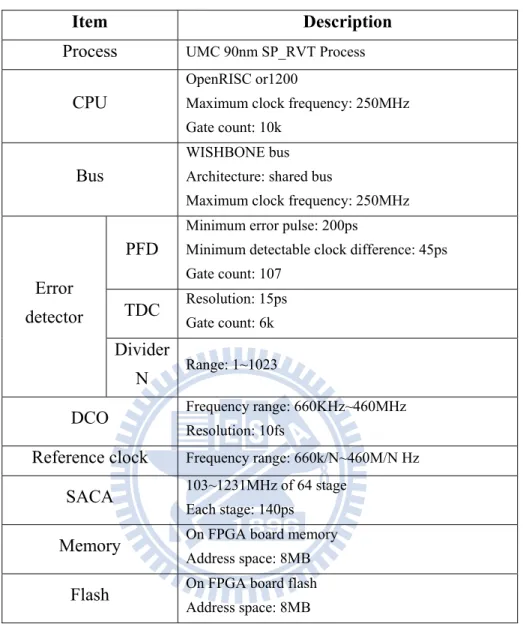
Table 1 Hardware specification
Item Description
Process UMC 90nm SP_RVT Process
CPU
OpenRISC or1200
Maximum clock frequency: 250MHz Gate count: 10k
Bus
WISHBONE bus Architecture: shared bus
Maximum clock frequency: 250MHz PFD
Minimum error pulse: 200ps
Minimum detectable clock difference: 45ps Gate count: 107 TDC Resolution: 15ps Gate count: 6k Error detector Divider N Range: 1~1023
DCO Frequency range: 660KHz~460MHz
Resolution: 10fs
Reference clock Frequency range: 660k/N~460M/N Hz
SACA 103~1231MHz of 64 stage
Each stage: 140ps
Memory On FPGA board memory
Address space: 8MB
Flash On FPGA board flash
Address space: 8MB
4.1.1. Memory Map
There are several I/O devices in MIMO-SDPLL. CPU needs access these devices from bus. The common method is that all I/O devices include memory are treated as a whole memory. Thus software can communication with specific hardware depends on this memory map. Fig.4.2 is the memory map at this work.
Fig.4.2 Memory map of 2×2 MIMO-SDPLL
4.1.2. CPU
The selection of CPU is OpenRISC or1200. Or1200 support cache, MMU and basic DSP capabilities. For direct use and area issue, the above function doesn’t implement in this work. By default configuration, the divided is simulation by multiplier with the help of compiler. It needs implement because the software is compiled without standard library. At UMC90 process, or1200’s gate count is 10k and has maximum frequency up to 250MHz.
4.1.3.
WISHOBONE Bus ProtocolFor CPU compatibility and IP cores connection, the WISHBONE [8] bus is chosen. WISHBONE has two type of interface: MASTER or SLAVE. MASTER can request transaction to SLAVE. Like CPU is a MASTER. SLAVE can reply transaction request from MASTER. All IP cores are SLAVE beside CPU in this work. Fig.4.3 shows a simple example of its single read and single write protocol. The bus protocol works as follows:
Single read-
CLK_I EDGE 0: MASTER presents a valid address on ADR_O. MASTER presents bank select SEL_O.
MASTER negates WE_O to indicate a read cycle. MASTER asserts STB_O to indicate the start of phase. MASTER asserts CYC_O to indicate the start of cycle.
CLK_I EDGE 1: SLAVE decodes input, and responding SLAVE asserts ACK_I. SLAVE presents a valid data on DAT_I.
MASTER monitors ACK_I, and prepares to latch data on DAT_I. Note: SLAVE can add any number of wait states (WSS) before asserts ACK_I. CLK_I EDGE 2: MASTER latches data on DAT_I.
MASTER negates STB_O and CYC_O to indicate the end of the cycle. SLAVE negates ACK_I in response to negated STB_O.
Single write-
CLK_I EDGE 0: MASTER presents a valid address on ADR_O. MASTER presents valid data on DAT_O. MASTER presents bank select SEL_O.
MASTER asserts WE_O to indicate a read cycle. MASTER asserts STB_O to indicate the start of phase. MASTER asserts CYC_O to indicate the start of cycle.
CLK_I EDGE 1: SLAVE decodes input, and responding SLAVE asserts ACK_I. SLAVE prepares to latch data on DAT_O.
MASTER monitors ACK_I, and prepares to terminate the cycle. Note: SLAVE can add any number of wait states (WSS) before asserts ACK_I. CLK_I EDGE 2: SLAVE latches data on DAT_O.
MASTER negates STB_O and CYC_O to indicate the end of the cycle. SLAVE negates ACK_I in response to negated STB_O.
CLK_I ADR_O DAT_I DAT_O WE_O SEL_O STB_O ACK_I CYC_O VALID
wss
wss
VALID VALID VALID VALID VALID READ WRITEFig.4.3 WISHBONE read / write timing graph
4.1.4. IP Cores Interconnection
In MIMO-SDPLL, the IP cores need be connected for communication. There are four defined types of WISHBONE interconnection, point-to-point, data flow, shared bus and crossbar switch. The shared bus and crossbar switch is useful for connecting two or more MASTERs with SLAVEs. They are suitable interconnection at this work. And the shared bus requires less interconnection logic and routing resources than crossbar switch. So the shared bus system is chosen for IP cores connection.
Fig.4.4 shows the interconnection block diagram. There two MASTERs and four SLAVEs. MASTERs include or1200’s data channel and instruction channel. SLAVEs include PLL module A, PLL module B, storage module and SACA module. PLL module is the combination of error detector module and DCO module. Storage module includes memory and flash.
The bus arbiter allocates the bus access priority between MASTERs, data channel priority is higher than instruction channel because of data dependency. The address comparator switches the correct data flow from MASTERs to SLAVEs according to the memory map in fig.4.2.
Fig.4.4. The interconnection block diagram of MIMO-SDPLL IP cores with shared bus system.
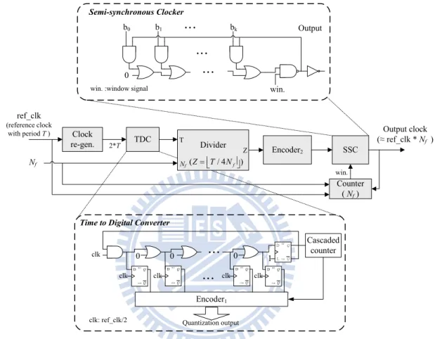
4.1.5. Semi-asynchronous clock access (SACA) module
It is important to decide the system clock in this work. There are two choices, one is reference clock and another is DCO clock. But reference clock is too slow and DCO clock is not stable enough for CPU computation. For this reason, the semi-asynchronous clock access (SACA) [3] is used.
SACA is a clock generator which synchronous to the rising edge of reference clock. And start trigger fixed number of cycles with specific period asynchronous to reference clock. The fixed number of cycles and clock period are defined by user. Fig.4.5 shows an example of SACA with four cycle count.
Fig.4.5. An example of SACA.
However, if the SACA clock frequency is higher than the frequency upper bond of system, the system will failed. To prevent this condition, the modified SACA architecture is proposed. In fig.4.6 shows the block diagram. It uses TDC, frequency divider, encoder and semi-asynchronous clocker (SAC) to generate the nearest clock. And this output clock will close to Nf × fref. Nf is the frequency multiplication factor define by user, fref is the reference
clock frequency. The output clock range of SACA is from 103MHz to 1231MHz into 64 stages, each stage is 140ps.
For example, if the reference clock is 30MHz and system needs 120MHz. The TDC will convert the reference clock period into digital data and divider will divide this data by four. Then encoder gets this divided-data and mapping it to the nearest clock of SAC. Finally, SAC
output the nearest clock about 30×4 = 120MHz for four cycles.
In this work, the Nf setting to more than 2048. Because the execution time of one
algorithm step needs less than one reference clock cycle.
TDC SSC ref_clk (reference clock with period T ) 2*T Output clock (≈ ref_clk * Nf ) Divider Nf (Z= ⎣⎢T/ 4Nf⎥⎦) Counter ( Nf) Encoder2 win. 0 … … b0 b1 … bk Output win. Semi-synchronous Clocker Z Nf T win. :window signal
Time to Digital Converter
Q Q SET CLR D Q Q SET CLR D Q Q SET CLR D Q Q SET CLR D Encoder1 Cascaded counter 0 0 … 0 … clk clk clk clk Quantization output clk SET CLR D L 1 Clock re-gen. clk: ref_clk/2
Fig 4.6. The modified SACA block diagram
4.2. Software
4.2.1. Software programming
The software programming environment lists in table 2. The working flows of software development are common. First, use C language to develop program. Second, compile the source code by gcc cross-compiler. Finally, gcc will generate executable binary file. This binary file will place in flash.
Table 2 Software environment
Item Description
Development language C
Cross compiler gcc 3.4.4 for OpenRISC 32 bit architecture
Host CentOS release 5.2 Kernel version: 2.6.18-92.1.17.el5
4.2.2. Memory map I/O control
In order to checking and setting hardware, the memory map I/O is used at this work. This manner help software programmer simpler and easier to access hardware IP cores. The memory map of IP cores shows in fig.4.2.
Here give an example of memory map I/O control. First, define the base address of IP core depend on fig.4.2.
#define DEVICE BASE ADDR x _ _ 0 95000000 (8) Second, declare a volatile pointer and assign base address value. A volatile qualifier must be used when reading the contents of a memory location whose value can change unknown to the current program.
* _ ;
_ = ( *) _ _ ;
volatile unsigned long DEVICE PTR
DEVICE PTR unsigned long DEVICE BASE ADDR (9)
Finally, this pointer can read or write IP cores register by software. / / _ * _ ; / / * _ _ ; = =
read hardware register data buf DEVICE PTR
write hardware register DEVICE PTR data buf
(10)
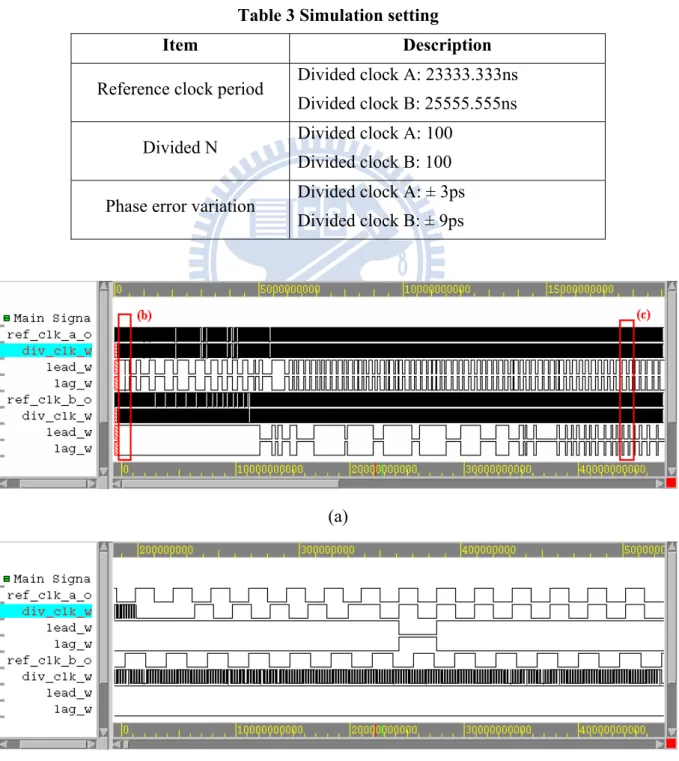
4.3. Simulation Result
This section shows the simulation result. The simulation setting lists in table 3. The simulation waveform is presented at fig.4.7. Because the waveform is hard to observation, the phase error information is recoded to draw a curve. This is helpful for the variation of phase
error. Fig.4.8 shows the result of phase error variation graph. X-axis represents number of reference clock; this is unrelated to clock period. Y-axis represents phase error between Nth reference clock and Nth divided clock in picoseconds. The above figures shows clock B start
tracking after clock A reaching phase maintain state. And both clock convergence at 550th
reference clock. The figure below shows the detail of 550th and 800th. The divided clock A
maintain at ± 3ps and clock B at ± 9ps.
Table 3 Simulation setting
Item Description
Reference clock period Divided clock A: 23333.333ns
Divided clock B: 25555.555ns
Divided N Divided clock A: 100
Divided clock B: 100
Phase error variation Divided clock A: ± 3ps
Divided clock B: ± 9ps
(a)
(c)
Fig.4.7. The waveforms of simulation result.
(a) The full view of waveform. (b) The zoom version of (a). Clock A do coarse tracking. (c) The zoom version of (c). Clock A and B enter frequency maintain stage.
Chapter 5
Conclusion and Future Work
From the simulation result, the proposed 2×2 MIMO- SDPLL has high resolution under software control. And more than one clock can be handled with scheduling. When the specification needs substantially modify, platform can fit the new specification by replacing the software.
In the future, the CPU scheduling can improve to multi-tasking. And the software development can provide different software IPs for different applications.
Reference
[1] Terng-Yin Hsu, Bai-Jue Shieh, Chen-Yi Lee” An all-digital phase-locked loop(ADPLL)-based clock recovery circuit” Solid-State Circuits, IEEE Journal of Volume 34, Issue 8, Aug. 1999 Page(s):1063-1073
[2] Ching-Che Chung, Chen-Yi Lee, “An all-digital phase-locked loop for high-speed clock generation” IEEE Journal of Solid-State Circuits, Vol38,pp.347-351, Feb.2003
[3] Chang-Ying Chuang, Terng-Yin Hsu” The Study of Software-defined Phase-locked loop ” Thesis CS, NCTU 2008.
[4] “OpenRISC 1200 IP Core Specification” Rev. 0.7, Sep 6, 2001 [5] “OpenRISC 1000 Architecture Manual “July 13, 2004
[6] Li Jyun-Rong, Hsu Terng-Yin” The Study of All Digital Phase-Locked Loop (ADPLL) and its Applications” Thesis CS, NCTU 2006.
[7] Jung-Chin Lai, Terng-Yin Hsu” The study of Wideband, Cell-based Digital Controlled Oscillator and its Implementation” Thesis CS, NCTU 2007.
[8] “WISHBONE System-on-Chip (SoC) Interconnection Architecture for Portable IP Cores” Revision: B.3, Released: September 7, 2002