Coplanar-Waveguide-Fed Microstrip Bandpass Filters
With Capacitively Broadside-Coupled Structures
for Multiple Spurious Suppression
Chi-Hsueh Wang, Member, IEEE, Pu-Hua Deng, and Chun Hsiung Chen, Fellow, IEEE
Abstract—Coplanar-waveguide (CPW)-fed microstrip bandpass filters are proposed with capacitive couplings suitably introduced at the input/output (I/O) ports, as well as between the resonators for spurious suppression. By adopting these capacitive couplings, several open stubs are established so that adjustable multiple transmission zeros may independently be created to suppress several unwanted spurious passbands, thereby extending the stopband and improving the rejection level. In this study, the capacitive couplings required at the I/O ports, as well as across the resonators, are realized by the broadside-coupled transition structures between the top microstrip layer and the bottom CPW layer so that the I/O ports may properly be matched and the spurious responses may effectively be suppressed. Specifically, a fifth-order bandpass filter, centered at 0 = 1 33 GHz with a stopband extended up to 8.67 GHz (6.52 0) and a rejection level better than 30 dB, is implemented and carefully examined.
Index Terms—Bandpass filter, coplanar waveguide (CPW), dual metal-layer structure, microstrip, spurious suppression.
I. INTRODUCTION
I
N MICROWAVE communication systems, the filters with deep stopband and good selectivity are required to enhance the system performance. In order to reduce the interference by keeping the out-band signals from reaching a sensitive receiver, a high-performance filter with wider upper stopband is also required. However, the planar bandpass filters made of half-wavelength uniform-impedance resonators have un-wanted spurious passbands at the multiples of center frequency , where is the passband center frequency. Several filters using the stepped-impedance resonators were proposed to shift the spurious passbands to the higher frequen-cies so as to extend the upper rejection band [1]–[3]. However, the stepped-impedance method can only push the spurious passbands to the higher frequencies instead of suppressing them. If one would like to move the first spurious passband to , e.g., by using the stepped-impedance resonators, a large impedance ratio for the resonators is required such that the layout of the filter becomes difficult due to the fabrication limit.Manuscript received August 18, 2006; revised October 26, 2006. This work was supported by the National Science Council of Taiwan under Grant NSC 94-2752-E-002-001-PAE, Grant NSC 94-2219-E-002-008, and Grant NSC 94-2213-E-002-055.
The authors are with the Department of Electrical Engineering and Graduate Institute of Communication Engineering, National Taiwan University, Taipei 106, Taiwan, R.O.C. (e-mail: [email protected]).
Digital Object Identifier 10.1109/TMTT.2007.892816
To solve these drawbacks, several methods to suppress spurious passbands have been reported [4]–[12]. In [4], the “wiggly-line” filters using a sinusoidally varying linewidth were proposed to give an effective suppression on the first spurious response around . Corrugated coupled microstrip lines [5]–[7] that are designed to equalize the phase velocities of the two eigenmodes were adopted to design the planar filters with suppression of the first spurious passband. In [8], an over-coupled resonator was employed to increase the electrical length of the odd mode so as to compensate for the difference in the phase velocities. Alternatively, the ideas of proposing substrate suspension [9] and ground-plane aperture [10] were reported to equalize the even- and odd-mode phase velocities so that the first spurious response can be suppressed. By etching split-ring resonators [11] to achieve strong magnetic coupling, the first spurious passband may also be suppressed. In [12], a meandered parallel coupled-line structure was utilized to sup-press the first spurious passband of a microstrip bandpass filter. However, most of these filter configurations still suffer from the higher order spurious responses around
[4]–[12].
The concept of using dissimilar resonators to produce dif-ferent harmonic frequencies for each resonator was proposed [13]–[15]. Based on this concept, one may implement a wide-stopband microstrip bandpass filter for which the spurious re-sponses may be suppressed due to the mutual cancellation ef-fect. However, the technique of adopting dissimilar resonators is not feasible in controlling the bandwidth of stopband and it would also suffer from the difficulty of choosing the proper dis-similar resonators to avoid the mutual coupling effects in the higher order filter design.
Recently, a coplanar waveguide (CPW) bandpass filter with rejection band extended up to was reported [16]. This filter is mainly composed of two parts, i.e., the loaded air-bridge en-hanced capacitors to suppress the lower order spurious pass-bands and the broadside-coupled microstrip-to-CPW-fed struc-tures to attenuate the high-order spurious responses, therefore, its stopband may be extended even up to . Although the method adopted by [16] is useful in realizing a very-wide stop-band CPW filter, it is difficult to extend to the other structures using different configurations.
In [17] and [18], capacitive-tapped couplings between res-onators and input/output (I/O) were established so that extra transmission zeros in the stopband can easily be created without requiring complex couplings between resonators. Here, tapped chip capacitors were inserted between the resonators, thus the
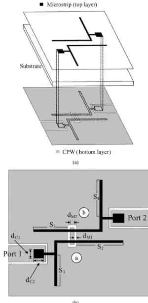
resonators (such as the one shown in Fig. 1) with capaci-tive couplings for multiple spurious suppression are proposed and carefully examined. First, the I/O capacitive couplings are achieved by using the broadside-coupled CPW-to-mi-crostrip transition structures [20] to replace the two I/O matched transformers adopted in [19] so that the I/O ports may properly be matched and the filter size may be reduced. These two I/O capacitive-coupled structures may also provide two open stubs to create two transmission zeros for spurious suppression. Second, the capacitive couplings between the adjacent resonators are realized by the broadside-coupled microstrip-to-CPW-to-microstrip transition structures instead of the parallel-coupled-line structures used in [19] so that extra open stubs may be created to produce additional transmission zeros for spurious suppression.
At first glance, the proposed filter (Fig. 1) might look sim-ilar to the dual-behavior resonator (DBR) filter discussed in [21]; however, they are quite different in topology and func-tion. Briefly, the DBR filters are based on the parallel associ-ation of two stopband structures which are carefully designed to create two transmission zeros on either side of the passband. By using the stepped-impedance and different-length stubs, the lengths of associated open or shorted stubs may be adjusted in-dependently, thus the created transmission zeros may be con-trolled freely. The main drawback of DBR filters concerns the attenuated band which is difficult to control over a wide range of frequencies, and this drawback may be solved by some spe-cial techniques [21]. The proposed filter topology is originated from the hairpin coupled-resonator filter. By using the capac-itively broadside-coupled structures for feeding and coupling, several open stubs can freely be established so as to create ad-justable multiple transmission zeros for suppressing several un-wanted spurious responses, therefore, the rejection level can be improved and the stopband can be extended even higher than , as will be demonstrated later. Moreover, the lengths and other parameters of open stubs may be adjusted, thus one may easily control the locations and widths of the attenuation dips in the filter response.
In comparison with the techniques used in [13]–[15] and [16], the method proposed in this study is easy in extension and simple in controlling the bandwidth of stopband. The proposed method would have a limitation in implementing a wide stopband filter, as did the one in [16], due to the difficulty in realizing the open stubs of very short lengths.
In this study, the basic principle of spurious suppression is demonstrated by implementing a second-order microstrip band-pass filter, which has four open stubs to create four transmis-sion zeros for supprestransmis-sion of spurious passbands. Specifically, a fifth-order microstrip bandpass filter is implemented, having ten open stubs to create five pairs of transmission zeros. Each
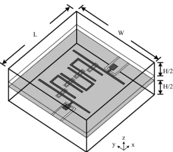
Fig. 1. Proposed second-order bandpass filter with capacitively broadside-cou-pled structures for feeding and coupling. (a) 3-D circuit layout. (b) Top-/bottom-layer circuit layouts to show the relative location between top microstrip Top-/bottom-layer and bottom CPW layer.
pair of transmission zeros is designed to suppress one spurious passband; thus, the implemented fifth-order filter may suppress five spurious passbands.
II. SECOND-ORDERFILTERS
A. Filter Structure and Design
The proposed second-order coupled-resonator microstrip bandpass filter structure composed of resonators is shown in Fig. 1 in which capacitively broadside-coupled structures are utilized to establish the proper feed circuits for I/O ports and the required couplings between the adjacent resonators. The relative location between the top microstrip layer and bottom CPW layer is shown in Fig. 1(b). Here, the broadside-coupled CPW-to-microstrip transition structures are employed to realize the I/O capacitive couplings instead of using two trans-formers in [19] so that the I/O ports may properly be matched and the filter size may be reduced. The I/O coupled structures
Fig. 2. Capacitively broadside-coupled microstrip-to-CPW-to-microstrip tran-sition structure and the associated open stubs of lengthsS and S . (W = W = 1:2 mm, d = 0:4 mm, and d = 0:9 mm).
provide two open stubs for producing two transmission zeros. The coupling between resonators and is realized by the capacitively broadside-coupled microstrip-to-CPW-to-mi-crostrip transition structure, which also supplies two open stubs for spurious suppression. Being composed of resonators, the proposed filter in Fig. 1 would exhibit the
spurious responses around .
The open stubs, such as , and in Fig. 1, are mainly introduced for spurious suppression. To this end, each open stub should properly be designed such that its length is equal to at the spurious frequency ; therefore, it would create a transmission zero designed to suppress the spu-rious passband around . The width of the open stub, which is related to the impedance of the transmission line in the stub, can determine the width and sharpness of the attenuation dip associated with the filter response in the stopband. For design purposes, the response to the broadside-coupled microstrip-to-CPW-to-microstrip transition structure shown in Fig. 2 needs to be investigated. Typical design curves presenting the relations between the transmission-zero frequencies and the lengths and of open stubs are shown in Fig. 3(a) and (b). Based on these design curves, the proper stub lengths and to locate the transmission zeros around may then be determined.
The capacitive coupling between adjacent resonators, such as resonators and , is established by the broadside-coupled mi-crostrip-to-CPW-to-microstrip transition structure, as depicted in Fig. 1. The corresponding coupling coefficient would specify the required coupling capacitance between the two adjacent res-onators, thereby determining the associated broadside-coupled structure between resonators. For example, the coupling coeffi-cient of the filter in Fig. 1 may be adjusted by varying the coupling capacitor between resonators and with its capaci-tance value mainly decided by the width in Fig. 1(b). The design curve for versus is shown in Fig. 4 for further reference.
To design the proposed bandpass filter (Fig. 1) with its pass-band center frequency at , each resonator is selected so that its resonant frequency is equal to the specified center fre-quency . Note that the lengths of open stubs and have already been decided by the spurious frequencies ) under rejection. To make sure that resonator in Fig. 1 is res-onated at the specified center frequency , the remaining length extracting and should be chosen such that the total length of resonator is equal to at . Obviously, through using
Fig. 3. (a) Full-wave simulated responses of the capacitively broadside-cou-pled transition structure in Fig. 2 (W = W = 1:2 mm). (b) Design curves to relate the transmission-zero frequenciesfz ; fz to the length S of open stub in Fig. 2. (S = 20 mm.)
Fig. 4. Coupling coefficientM versus the width d [see Fig. 1(b)] of the coupled structure between resonatorsa and b. (d = 0:4 mm.)
the broadside-coupled elements, the choice of the stubs’ length is free and not dependent on the design of resonator. Although
Fig. 5. Feed structure associated with the resonator near I/O port.
the transmission-zero frequencies due to the open stubs are far from the passband, the open stubs still have small influences on the resonance frequency of the resonator. This is why the lengths of open stubs should be decided at the first design step, and, in the meantime, one should make sure that the total length of each resonator is equal to at . These small influences will be considered using the transmission line model.
The feed structure associated with the resonator near the I/O port should properly be designed so as to give the specified ex-ternal quality factor . The value of the external quality factor would be determined from the filter specification. Fig. 5 shows the proposed feed structure in which a capacitor and suit-able transmission line sections are adopted for I/O coupling and impedance matching. This feed structure is connected to the res-onator for which its value is given by [19].
The load impedance , defined at point of Fig. 5, may be written as
(1) If this load impedance is not equal to 50 , a trans-former or J-inverter should be added for impedance matching [19]. Note that the series coupling capacitor together with two transmission line sections of characteristic impedance and length at its two ends may be equivalent to a J-inverter, as shown in Fig. 5, for impedance matching. Consequently, the required I/O coupling (or matching) capaci-tance and length may be given by
(2)
(3) where is the susceptance of the capacitance .
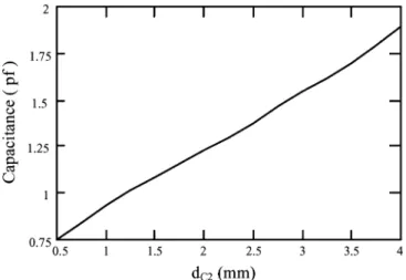
Fig. 6. Coupling capacitance versus the widthd [see Fig. 1(b)] of the I/O coupled structure. (d = 4:5 mm.)
The I/O capacitive coupling is realized by the parallel-plate capacitor structure with a size of , as shown in Fig. 1(b). The coupling capacitance versus the width is shown in Fig. 6.
Finally, the broadside-coupled CPW-to-microstrip transition structures (J-inverters) are introduced at the input and output so that the I/O ports may properly be matched.
The design guidelines for the proposed coupled-resonator bandpass filters, such as the one in Fig. 1, are summering in the following.
• The first step is to design each open stub associated with the resonators so that it would create a transmission zero to suppress the spurious passband around ). • The second step is to design the filter resonators so as to
meet the given specifications.
• The third step is to implement the required coupling coef-ficients between the adjacent resonators so as to meet the bandwidth specification for the filter.
• The last step is to deal with the feed structure using (1)–(3).
B. Filter Implementation and Results
The proposed CPW-fed second-order microstrip bandpass filter with capacitively broadside-coupled transition struc-ture between adjacent resonators is fabricated on the Rogers
RO4003C substrate ( , and thickness
mm). Fig. 1 shows the 3-D and top-/bottom-layer layouts of the proposed second-order microstrip bandpass filter. The implemented filter has a dimension of
(40.4 mm 53 mm), where is the guided wavelength of the microstrip structure at the center frequency . This filter is designed according to the second-order maximally flat response with a center frequency of 1.45 GHz and a 3-dB bandwidth of 12%, for which the coupling coefficient is 0.083. The specific dimension [see Fig. 1(b)] to give the required may be determined from Fig. 4.
The external quality factors at input and output are 12.8. The required coupling capacitances at input and output are 1.34 and 1.49 pF, respectively, and their values may be calculated by (2). The required dimension [see Fig. 1(b)], which estab-lishes the desired value is given in Fig. 6. The corresponding
Fig. 7. Measured and simulated results, insertion loss (j S j), and return loss (j S j) of the proposed second-order filter in Fig. 1. (a) Narrowband and (b) wideband frequency responses.
geometrical parameters are then fine tuned in the full-wave sim-ulator Ansoft Ensemble 8.0.
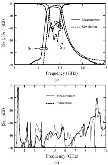
The measured and simulated results of the implemented filter (Fig. 1) are shown in Fig. 7. The measured center frequency is at 1.43 GHz and the minimum insertion loss is 1 dB. Four trans-mission zeros are produced by the four open stubs , , , and (Fig. 1) and are found at 2.33, 2.66, 4.51, and 4.85 GHz, respectively. The shift in these transmission-zeros frequencies is less than 5%.
The sensitivity of this proposed filter is mainly dependent on the fabrication process. Normally the fabrication error associ-ated with the size is approximately 0.0254 mm and the cor-responding electrical length error is 1 at 20 GHz. Thus, the proposed filter would have a limitation in extending the band-width of stopband due to the difficulty in realizing the open stubs of very short lengths.
The second filter structure, shown in Fig. 8, has four trans-mission zeros designed to suppress the first spurious passband. This implemented filter has a dimension of
(28.1 mm 41.9 mm). Specifically, the two transmission zeros associated with the two open stubs and are distributed around 3.4 GHz and the other two zeros produced by the two
Fig. 8. Top-/bottom-layer layouts of the second-order filter with four transmis-sion zeros to distribute around the first spurious passband.
stubs and are distributed around 3.6 GHz. This filter is also designed according to the second-order maximally flat re-sponse with a center frequency of 1.44 GHz, a 3-dB bandwidth of 13.5%, and the required coupling coefficient is 0.0954. The external quality factors at input and output are 10.47. The coupling capacitances at input and output are 1.44 pF. The measured and simulated results of the second filter (Fig. 8) are shown in Fig. 9. The measured center frequency is at 1.43 GHz, the minimum insertion loss is 1.05 dB. The frequency response for the filter in Fig. 1 is also compared with that for Fig. 8. With four transmission zeros designed for the first spurious harmonic, the filter in Fig. 8 has much better rejection around this har-monic, as shown in Fig. 10.
III. FIFTH-ORDERFILTER
Fig. 11 shows the top-/bottom-layer layouts of the pro-posed fifth-order filter. Here, the capacitive couplings at I/O ports are again implemented by the broadside-coupled CPW-to-microstrip transition structures and those between adjacent resonators are by the broadside-coupled-microstrip-to-CPW-to-microstrip transition structures. This filter has ten open stubs to create ten transmission zeros, which are assigned to some specified frequencies. Specifically, the transmission zeros due to the stubs
and are designed to distribute around the first, second, third, fourth, and fifth spurious harmonics, respectively, so that five spurious passbands may effectively be suppressed.
The design guidelines for this fifth-order filter are similar to the ones for the second-order filter, as mentioned in Section II. The proposed filter is designed according to the fifth-order Chebyshev filter with a 0.1-dB ripple level, having a center frequency of 1.35 GHz and a 3-dB bandwidth of 10%. The required I/O coupling capacitances and coupling coefficients between adjacent resonators are obtained as in Section II, and the corresponding coupling coefficients
and are 0.077, 0.0583, 0.0583, and 0.077, respectively. The external quality factors at input and output are 11.8. The coupling capacitances at input and output are 1.51 pF.
Fig. 9. Measured and simulated results of the second-order filter in Fig. 8. (a) Narrowband and (b) wideband frequency responses.
Fig. 10. Comparison of the measured responses for the filters in Figs. 1 and 8.
The implemented filter has a dimension of (64.6 mm 56 mm).
The measured and simulated results for the implemented fifth-order filter (Fig. 11) are shown in Fig. 12. The measured center frequency is at 1.33 GHz and the minimum insertion loss is 2.92 dB. Good agreement between measured and simulated
Fig. 11. Top-/bottom-layer layouts of the proposed fifth-order filter for mul-tiple spurious suppression.
Fig. 12. Measured and simulated results of the proposed fifth-order filter in Fig. 11. (a) Narrowband and (b) wideband frequency responses.
results is observed, except for a slight frequency shift of less than 2% around passband. As shown in Fig. 12(b), the stopband
Fig. 13. Rectangular housing structure for the proposed fifth-order filter in Fig. 11. (W = 86 mm, L = 84:8 mm, H = 30 mm.)
Fig. 14. Simulated results of the fifth-order filter in Fig. 11 with and without housing. (Curve 1: with housing, but without absorber, Curve 2: with housing and absorber, Curve 3: without housing.)
is extended up to 8.67 GHz with a rejection level better than 30 dB. Note that the proposed fifth-order filter has suppressed the five spurious passbands.
To provide necessary support and to prevent unnecessary interferences, the filter is usually surrounded by a metallic housing in the system application. Physically, the housing may cause unwanted cavity resonances to degrade the spurious-sup-pression characteristic. Thus, the housing effect should be dealt with in the filter design phase. Note that the cavity resonances would eventually appear no matter how the housing is arranged and reshaped. Shown in Fig. 13 is a typical rectangular housing structure for the proposed fifth-order filter in Fig. 11. An approach to suppress the unwanted cavity resonances is to attach the absorbing material inside the housing walls [16]. Curve 1 of Fig. 14 exhibits the simulated result of the filter with the metallic housing (but without the absorbing material). Obviously, the spurious-suppression characteristic has been
destroyed due to the cavity resonances, and extra spurious passbands are observed around the resonant frequencies of the cavity. By attaching the absorbing material on the top and bottom walls of the housing, those unwanted resonances may be suppressed, as shown in the simulated Curve 2 in Fig. 14. Although the use of absorbing material may provide a solution for suppressing the unwanted cavity resonances, the lossy absorbing material would also increase the insertion loss of the filter. As shown in Fig. 14, the insertion loss of Curve 1 is 2.2 dB, but that of Curve 2 is 2.93 dB at the passband center frequency.
IV. CONCLUSION
In this paper, the CPW-fed microstrip bandpass filters have been implemented and carefully examined with capacitively broadside-coupled structures established at I/O ports and be-tween adjacent resonators so as to provide extra open stubs for spurious suppression. By adjusting the lengths of open stubs, multiple transmission zeros may be created and suitably distributed without increasing the circuit area so that multiple spurious passbands may effectively be suppressed and the rejection bandwidth may be extended. Specifically, a fifth-order bandpass filter, centered at GHz, has been imple-mented and its stopband has been extended up to 8.67 GHz (6.52 ) with a rejection level better than 30 dB.
REFERENCES
[1] M. Makimoto and S. Yamashita, “Bandpass filters using parallel cou-pled stripline stepped impedance resonators,” IEEE Trans. Microw. Theory Tech., vol. MTT-28, no. 12, pp. 1413–1417, Dec. 1980. [2] S. Y. Lee and C. M. Tsai, “New cross-coupled filter design using
im-proved hairpin resonators,” IEEE Trans. Microw. Theory Tech., vol. 48, no. MTT-12, pp. 2482–2490, Dec. 2000.
[3] C. M. Tsai, S. Y. Lee, and C. C. Tsai, “Performance of a planar filter using a 0 feed structure,” IEEE Trans. Microw. Theory Tech., vol. 50, no. 10, pp. 2362–2367, Oct. 2002.
[4] T. Lopetegi, M. A. G. Laso, J. Hernandez, M. Bacaicoa, D. Benito, M. J. Grade, M. Sorolla, and M. Guglielmi, “New microstrip ‘wiggly-line’ filters with spurious passband suppression,” IEEE Trans. Microw. Theory Tech., vol. 49, no. 9, pp. 1593–1598, Sep. 2001.
[5] J. T. Kuo, W. H. Hsu, and W. H. Hsu, “Parallel coupled microstrip filters with suppression of harmonic response,” IEEE Microw. Wireless Compon. Lett., vol. 12, no. 10, pp. 383–385, Oct. 2002.
[6] B. S. Kim, J. W. Lee, and M. S. Song, “An implementation of har-monic-suppression microstrip filters with periodic grooves,” IEEE Mi-crow. Wireless Compon. Lett., vol. 14, no. 9, pp. 413–415, Sep. 2004. [7] S. Sun and L. Zhu, “Periodically nonuniform coupled microstrip-line
filters with harmonic suppression using transmission zero reallo-cation,” IEEE Trans. Microw. Theory Tech., vol. 53, no. 5, pp. 1817–1822, May 2005.
[8] J. T. Kuo, S. P. Chen, and M. Jiang, “Parallel-coupled microstrip filters with over-coupled end stages for suppression of spurious responses,” IEEE Microw. Wireless Compon. Lett., vol. 13, no. 10, pp. 440–442, Oct. 2003.
[9] J. T. Kuo, M. Jiang, and H. J. Chang, “Design of parallel-coupled mi-crostrip filters with suppression of spurious resonances using substrate suspension,” IEEE Trans. Microw. Theory Tech., vol. 52, no. 1, pp. 83–89, Jan. 2004.
[10] M. d. C. Velazquez-Ahumada, J. Martel, and F. Medina, “Parallel coupled microstrip filters with ground-plane aperture for spurious band suppression and enhanced coupling,” IEEE Trans. Microw. Theory Tech., vol. 52, no. 3, pp. 1082–1086, Mar. 2004.
[11] J. Garacia-Garacia, F. Martin, F. Falcone, J. Bonache, I. Gil, T. Lopetegi, M. A. G. Laso, M. Sorolla, and R. Marques, “Spurious passband suppression in microstrip coupled line bandpass filters by means of split ring resonators,” IEEE Microw. Wireless Compon. Lett., vol. 14, no. 9, pp. 416–418, Sep. 2004.
[15] S. C. Lin, P. H. Deng, Y. S. Lin, C. H. Wang, and C. H. Chen, “Wide-stopband microstrip bandpass filters using dissimilar quarter-wave-length stepped-impedance resonators,” IEEE Trans. Microw. Theory Tech., vol. 54, no. 3, pp. 1011–1018, Mar. 2006.
[16] S. C. Lin, T. N. Kuo, Y. S. Lin, and C. H. Chen, “Novel coplanar-waveguide bandpass filters using loaded air-bridge enhanced capaci-tors and broadside-coupled transition structures for wideband spurious suppression,” IEEE Trans. Microw. Theory Tech., vol. 54, no. 8, pp. 3359–3369, Aug. 2006.
[17] K. Wada and I. Awai, “Heuristic models of half-wavelength resonator bandpass filter with attenuation poles,” Electron. Lett., vol. 35, no. 3, pp. 401–402, Mar. 1999.
[18] T. Ohno, K. Wada, and O. Hashimoto, “A class of a planar triplexer by manipulating multiple attenuation poles,” in Proc. 34th Microw. Eur. Conf., Amsterdam, The Netherlands, Oct. 2004, pp. 625–628. [19] J. T. Kuo and E. Shih, “Microstrip stepped impedance resonator
band-pass filter with an extended optimal rejection bandwidth,” IEEE Trans. Microw. Theory Tech., vol. 51, no. 5, pp. 1554–1559, May 2003. [20] K. M. Shum, T. T. Mo, Q. Xue, and C. H. Chan, “A compact bandpass
filter with two tuning transmission zeros using a CMRC resonator,” IEEE Trans. Microw. Theory Tech., vol. 53, no. 3, pp. 895–900, Mar. 2005.
[21] A. Manchec, C. Quendo, I.-F. Favennec, E. Rius, and C. Person, “Syn-thesis of capacitive-coupled dual-behavior resonator (CCDBR) filters,” IEEE Trans. Microw. Theory Tech., vol. 54, no. 6, pp. 2346–2355, Jun. 2006.
Chi-Hsueh Wang (S’02–M’05) was born in
Kaoh-siung, Taiwan, R.O.C., in 1976. He received the B.S. degrees in electrical engineering from National Cheng Kung University, Tainan, Taiwan, R.O.C., in 1997, and the Ph.D. degree from National Taiwan University, Taipei, Taiwan, R.O.C., in 2003.
He is currently a Post-Doctoral Research Fellow with the Graduate Institute of Communication Engi-neering, National Taiwan University. His research in-terests include the design and analysis of microwave and millimeter-wave circuits and computational elec-tromagnetics.
Chun Hsiung Chen (SM’88–F’96) was born in
Taipei, Taiwan, R.O.C., on March 7, 1937. He received the B.S.E.E. and Ph.D. degrees in electrical engineering from National Taiwan University, Taipei, Taiwan, R.O.C., in 1960 and 1972, respec-tively, and the M.S.E.E. degree from National Chiao Tung University, Hsinchu, Taiwan, R.O.C., in 1962.
In 1963, he joined the Faculty of the Department of Electrical Engineering, National Taiwan University, where he is currently a Professor. From August 1982 to July 1985, he was Chairman of the Department of Electrical Engineering, National Taiwan University. From August 1992 to July 1996, he was the Director of the University Computer Center, National Taiwan University. In 1974, he was a Visiting Scholar with the Department of Electrical Engineering and Computer Sciences, University of California at Berkeley. From August 1986 to July 1987, he was a Visiting Professor with the Department of Electrical Engineering, University of Houston, Houston, TX. In 1989, 1990, and 1994, he visited the Microwave Department, Technical University of Munich, Munich, Germany, the Laboratoire d’Optique Electromagnetique, Faculte des Sciences et Techniques de Saint-Jerome, Universite d’Aix-Marseille III, Mar-seille, France, and the Department of Electrical Engineering, Michigan State University, East Lansing, respectively. His areas of interest include microwave circuits and computational electromagnetics.
![Fig. 4. Coupling coefficient M versus the width d [see Fig. 1(b)] of the coupled structure between resonators a and b](https://thumb-ap.123doks.com/thumbv2/9libinfo/8820440.232021/3.891.458.826.787.1034/fig-coupling-coefficient-versus-width-coupled-structure-resonators.webp)