Infrared emission from Ge metal-insulator-semiconductor tunneling diodes
M. H. Liao
Department of Electrical Engineering, National Taiwan University, Taipei, Taiwan 106, Republic of China and Graduate Institute of Electro-Optical Engineering, National Taiwan University, Taipei, Taiwan 106, Republic of China
T.-H. Cheng
Department of Electrical Engineering, National Taiwan University, Taipei, Taiwan 106, Republic of China and Graduate Institute of Electronics Engineering, National Taiwan University, Taipei, Taiwan 106, Republic of China
C. W. Liua兲
Department of Electrical Engineering, National Taiwan University, Taipei, Taiwan 106, Republic of China; Graduate Institute of Electro-Optical Engineering, National Taiwan University, Taipei, Taiwan 106, Republic of China; and Graduate Institute of Electronics Engineering, National Taiwan University, Taipei, Taiwan 106, Republic of China
共Received 22 August 2006; accepted 15 November 2006; published online 28 December 2006兲 The Ge light-emitting diode with ⬃1.8 m strong infrared emission is demonstrated using a metal-insulator-semiconductor tunneling structure. The intensity of a Ge device is one order of magnitude stronger than a similar Si device. At the positive gate bias, the holes in the Al gate electrode tunnel to the n-type Ge through the ultrathin oxide and recombine radiatively with electrons. An electron-hole-plasma model can be used to fit all the emission spectra from room temperature down to 65 K. From the measurement temperature range, the extracted band gap is ⬃40 meV lower than the reported band gap data, and the linewidth drops from 70 to 25 meV. The longitudinal acoustic phonon 共⬃28 meV兲 and/or the band gap renormalization at high carrier density are proposed to be responsible for the reduction of photon energy. The band gap reduction on the mechanically strained n-type Ge and Si is also investigated experimentally and theoretically. © 2006 American Institute of Physics. 关DOI:10.1063/1.2420783兴
Much effort has been devoted in seeking the possibilities of light emission using indirect band gap materials1–4 for both scientific interest and optoelectronic applications. The 1.1m infrared emission from Si using the metal-insulator-semiconductor 共MIS兲 tunneling structure was demonstrated in the past.5 By the Ge incorporation, the emission wave-length can be further tuned. The infrared emissions of⬃1.3, ⬃1.5,6
and ⬃2 m7 wavelengths from Si0.8Ge0.2 quantum well, Si0.45Ge0.55 quantum dot, and Si/ SiGe heterojunction, respectively, were also reported using a similar MIS tunnel-ing structure. Due to the high carrier mobility, strong photon absorption,8and possible integration with Si, the light emis-sion from Ge is of great interest for scientific research and practical applications. In this letter, the 1.8m infrared emission from Ge MIS tunneling diode with the effects of temperature and strain is investigated. As compared with the similar Si device, the infrared emission of Ge device is much stronger共approximately ten times higher兲. The strain effect on Ge band gap reduction is less severe than that of Si and is consistent with the theoretical calculation.
The 2 nm oxide used in the MIS tunneling diode is grown by liquid phase deposition共LPD兲 at 50 °C on n-type Ge共100兲 wafer.9The resistivity of the 100 mm Ge wafer is in the range of 0.04– 0.4⍀ cm. Before oxide deposition, the sample was cleaned by a HF dip. The thickness is measured by an ellipsometer. The MIS tunneling diode has Al gate electrodes with the circular area defined by the shadow mask.
The other Al contact is on the back of the wafer. The experi-mental setup for measuring the electroluminescence 共EL兲 spectra and Raman spectra, and the mechanism to apply ex-ternal mechanical strain are similar to the methods used in Refs.10and11.
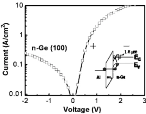
Figure 1shows the typical I-V curve of a Ge MIS tun-neling diode. When the Al gate is at negative gate bias, the current is mainly controlled by the thermally generated holes.12 For the positive bias, the holes in the Al gate elec-trode tunnel into the Ge, besides the electron tunneling from the Ge to the Al gate electrode. As a result, a significant tunneling current was observed at the positive gate bias. Meanwhile, the positive gate bias also attracts electrons in the Ge/oxide interface to form an accumulation layer. The momentum spread due to the localized electrons in the accu-mulation layer, phonons, and the Ge/oxide interface
rough-a兲Author to whom corresponding should be addressed; electronic mail:
FIG. 1. I-V curve of a metal-insulator n-type Ge tunneling diode. The inset shows the schematic band diagram at the accumulation positive bias. APPLIED PHYSICS LETTERS 89, 261913共2006兲
0003-6951/2006/89共26兲/261913/3/$23.00 89, 261913-1 © 2006 American Institute of Physics
ness can provide the necessary momentum during the electron-hole radiative recombination.5 The luminescence was collected when the tunneling holes from Al gate elec-trode to Ge radiatively recombine with the electrons in the accumulation region of Ge. The band diagram of the Ge MIS light emitting diode共LED兲 at the positive gate bias is shown as the inset of Fig. 1 for reference. For the MIS tunneling diode with a positive gate bias, intensive infrared共Fig.2兲 is emitted with a peak around 1.8m 共0.7 eV兲. In order to compare the external quantum efficiency between Ge and Si MIS LEDS, two kinds of MIS tunneling diodes were fabri-cated by the same process, gate electrode, and LPD oxide thickness 共⬃2 nm兲 which is controlled by the deposition time. The optical power from Si MIS LED and Ge MIS LED can be detected by two different commercial InGaAs p-i-n diodes. The spectral range of InGaAs detectors covers from 0.95 to 1.6m 共with the responsivity of 0.65 A/W at 1.1m兲 and from 1.2 to 2 m 共with the responsivity of 1.1 A / W at 1.8m兲 for Si and Ge MIS LED measurements, respectively. The resulting current was read by Keithley 485 picoammeter. Under the injection current of 100 mA, the ex-ternal quantum efficiency for⬃1.8m light emission from the Ge MIS LED is observed as⬃5⫻10−5at room tempera-ture, about one order of magnitude higher than Si MIS LED at the same measurement condition. It may be due to the higher radiative recombination coefficient of Ge 共6.4 ⫻10−14cm3s−1for Ge and 1.1⫻10−14cm3 s−1for Si兲 共Ref.
13兲 and the slightly smaller wave vector k needed to con-serve momentum in Ge. However, the clear origin is still unknown and worthy of investigation. Note that in our quan-tum efficiency measurement, we cannot collect all the light from the device, and only the scattered light from the periph-ery of the gate area was detected. Therefore, the number presented here is a lower bound of the true quantum effi-ciency. The feature of the emission line shape is the asym-metrical broadening, where the high energy part is broader than the low-energy part. This is very similar to the line shape of the electron-hole-plasma 共EHP兲 recombination in Si.5To confirm this observation, the line shape of EL spectra 共Fig.2兲 is fitted by the EHP recombination model using the following expression:
I共h兲 = I0
冕
0
h−Eg,EL
dEDe共E兲Dh共h− Eg,EL
− E兲fe共E,Fe,T兲fh共h− Eg,EL− E,Fh,T兲,
where Deand Dhare the densities of states of electrons and
holes, respectively, Feand Fhare the respective quasi-Fermi
energies, h is the energy of photon emitted, T is the mea-surement temperature, Eg,ELis the band gap of Ge obtained
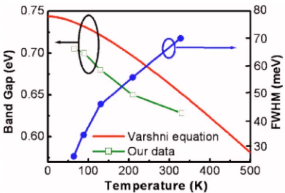
by the EL measurement, and f are the Fermi-Dirac distribu-tion. The fitting parameters used in this work are also listed in Fig.2. The carrier density estimated from the quasi-Fermi energy at 65 K is about 8⫻1017 cm−3. According to the Mott transition, excitons will dissociate into electron-hole plasma at a high carrier density. The extracted band gaps from the EL spectra from Ge MIS tunneling diode are ⬃40 meV lower than the Ge band gap obtained from Varshni’s equation14 for the measurement temperatures共Fig.3兲, while the photon energy reduction in Si MIS tunneling diode is observed to be⬃80 meV.15 The phonon replicas can be in-volved in the momentum conservation of the radiative re-combination and should be responsible for the photon energy reduction. In Ge, the longitudinal acoustic 共LA兲 phonons 共 ⬃28 meV兲 are strongest and prominent, while the transverse optical phonons共⬃58 meV兲 are favored in Si.16On the other hand, the high carrier concentration of ⬃8⫻1017cm−3 causes further energy reduction of⬃7 meV for Ge devices, based on the band gap renormalization model calculation.17 The rest of band gap lowering共⬃5 meV兲 maybe due to the surface bending15 or extraction errors. The band gap renor-malization of Ge is less serve than that of Si.17–19The line-width 共full width at half maximum兲 of the EL spectra de-creases from 70 to 25 meV when the temperature dede-creases from room temperature to 65 K 共Fig.3兲. The carrier filling closer to the conduction-band and valence-band edges at lower temperature is responsible for the decrease in line-width.
Figure 4 shows the EL spectra at 65 K from the un-strained and un-strained Ge MIS LEDs. The magnitude of strain is measured by Raman spectroscopy. Raman spectra were excited by an Ar laser共wavelength of 514 nm兲 and the Ra-man shifts of 0.91 and 1.32 cm−1under uniaxial and biaxial tensile strains, respectively, were extracted from the curve fitting using a Lorentzian profile.11Using the Raman shift of the Ge-Ge phonon peak and phenomenological potentials, the strains in Ge are estimated to be 0.32% for biaxial strain and 0.45% for uniaxial strain,11respectively. The redshift of the EL spectra under the external tensile strain was observed in Ge MIS LED, similar to the Si MIS LED.10 The peak of
FIG. 2. Measured electroluminescence spectra of a bulk Ge共100兲 metal-insulator-semiconductor light-emitting diode at different temperatures. The fitting parameters such as temperature and the band gap of EL spectra are also listed for reference.
FIG. 3. Extracted band gap and linewidth at different temperatures.
261913-2 Liao, Cheng, and Liu Appl. Phys. Lett. 89, 261913共2006兲
the light emission spectra at the temperature of 65 K is re-duced by 30 meV共69 nm兲 under the 0.32% external biaxial tensile strain. Band gap reduction as a function of external strain for Ge and Si is shown in Fig.5 with the theoretical curves. Both Ge and Si band gaps are reduced under the tensile strain. Using the deformation potential parameter in Ref.19, with the formula in Ref.20, the theoretical values of band gap reduction共⌬Eg兲 of Ge 共Si兲 due to external strain
are calculated to be −80共−105兲 meV/% for the biaxial ten-sile strain and −15共−60 meV/% for the uniaxial tenten-sile strain, very close to the experimental data.
In summary, we presented the EL spectra from the EHP recombination in the Ge MIS tunneling diode at different temperatures. The EL spectra can be fitted by a simple con-volution of electron and hole distribution functions. The LA phonon and/or the band gap renormalization at high carrier density may be responsible for the reduction in Ge. With the external strain, the emission wavelength can be further turned.
This work is supported by the National Science Council of ROC under Contract Nos. 2221-E-002-370 and 95-2221-E-002-357.
1H. Mimura, T. Matsumoto, and Y. Kanemitsu, Appl. Phys. Lett. 65, 3350
共1994兲.
2Q. Mi, X. Xiao, J. C. Sturm, L. C. Lenchyshyn, and M. L. W. Thewalt,
Appl. Phys. Lett. 60, 3177共1992兲.
3H. Presting, T. Zinke, A. Splett, H. Kibbel, and M. Jaros, Appl. Phys. Lett. 69, 2376共1996兲.
4W. Eisfeld, U. Werling, and W. Prettl, Appl. Phys. Lett. 42, 276共1983兲. 5C. W. Liu, M. H. Lee, M.-J. Chen, I. C. Chen, and C.-F. Lin, Appl. Phys.
Lett. 76, 1516共2000兲.
6M. H. Liao, C.-Y. Yu, T.-H. Guo, C.-H. Lin, S. T. Chang, C.-T. Chai, and
C. W. Liu, IEEE Electron Device Lett. 27, 252共2006兲.
7M. H. Liao, C.-Y. Yu, C.-F. Huang, C.-H. Lin, C.-J. Lee, M.-H. Yu, S. T.
Chang, C.-Y. Liang, C.-Y. Lee, T.-H. Guo, C.-C. Chang, and C. W. Liu, Tech. Dig. - Int. Electron Devices Meet. 2005, 1023.
8Y.-H. Kuo, Y. K. Lee, Y. Ge, S. Ren, J. E. Roth, T. I. Kamins, D. A. B.
Miller, and J. S. Harris, Nature共London兲 437, 1334 共2005兲.
9P.-S. Kuo, B.-C. Hsu, P.-W. Chen, P. S. Chen, and C. W. Liu, Electrochem.
Solid-State Lett. 7, G201共2004兲.
10M. H. Liao, M.-J. Chen, T. C. Chen, P.-L. Wang, and C. W. Liu, Appl.
Phys. Lett. 86, 223502共2005兲.
11M. H. Liao, P.-S. Kuo, S.-R. Jan, S. T. Chang, and C. W. Liu, Appl. Phys.
Lett. 88, 143509共2006兲.
12B.-C. Hsu, W. T. Liu, C.-H. Lin, and C. W. Liu, IEEE Trans. Electron
Devices 48, 1747共2001兲.
13http://www.ioffe. rssi. ru/SVA/NSM/Semicond/
14S. M. Sze, Physics of Semiconductor Devices, 2nd ed.共Wiley, New York,
1981兲, p. 15.
15C. W. Liu, M.-J. Chen, I. C. Chen, M. H. Lee, and C.-F. Lin, Appl. Phys.
Lett. 77, 1111共2000兲.
16J. Weber and M. I. Alonso, Phys. Rev. B 40, 5683共1989兲. 17D. A. Kleinman, Phys. Rev. B 33, 2540共1986兲.
18X. Xiao, C. W. Liu, J. C. Sturm, L. C. Lenchyshyn, and M. L. W. Thewalt,
Appl. Phys. Lett. 60, 1720共1992兲.
19Properties of Crystalline Silicon, EMIS Datareviews Series No. 20, edited
by R. Hull共INSPEC, London, 1999兲, p. 404.
20C. G. Van der Walle, Phys. Rev. B 39, 1871共1989兲.
FIG. 4. Electroluminescence spectra of the Ge metal-insulator-semiconductor light-emitting diode under 0.32% biaxial tensile strain at 65 K.
FIG. 5. Band gap reduction of strained Ge and Si due to strain. Biaxial strain gives more band gap reduction than uniaxial strain, and the reduction of Ge band gap is less than Si band gap under external strain.
261913-3 Liao, Cheng, and Liu Appl. Phys. Lett. 89, 261913共2006兲