1.中文摘要 隨著元件與效能的持續改善,金屬層間介電層也逐漸的採用低介電常數材 料。而在本研究中,針對兩種介電材料 SiLK 和 SiO2的熱特性與金屬層的抗電遷 移的研究,這可以評估低介電常數材料 SiLK 作為金屬層間介電層的可行性。利 用舉離法來製作測試電遷移的銅導線,利用田口法來求得最佳的實驗參數。由本 研究可以得到,利用 SiLK 作為金屬層間介電層的熱阻抗較 SiO2作為金屬層間介 電層高 14%。依據熱阻抗與導線溫度上升的狀況,可以推斷主要的熱量轉移是經 由金屬層下層介電層到達矽基板。而利用 SiLK 作為金屬層間介電層的對於電遷 移的活化能比起利用 SiO2作為金屬層間介電層還小,相對的生命期也較短,可 能的機制在本研究中討論。 而介電材料的介電非等向性也是介電材料利用在金屬層間介電層必須要考 慮的因素。利用兩種的測試結構可以估計 SiLK 的介電非等向性。金屬-介電質-金屬平行電容結構用來估計垂直介電係數,利用 comb-serpentine 叉合結構估計 平行介電係數。所以得到 SiLK 垂直介電係數為 2.65,介電非等向性為 3.85%。
然而,SiLK 的漏電流比 SiO2大,本研究中討論銅導線與 SiLK 整合的可靠度。
關鍵字:介電等向性,銅,銅與低介電常數材料的整合,電遷移,可靠度 2.Abstract
As device density and performance continue to improve, low dielectric constant (k) materials are needed for interlevel dielectric (ILD) applications. In this study, the thermal characteristics and electromigration (EM) resistance of two dielectrics, SiLKTM and SiO2, are investigated to evaluate the feasibility of low dielectric constant
dielectric SiLKTM for the intermetal dielectric applications. Lift-off patterning was employed to fabricate the Cu interconnect for EM test and Taguchi method was used in the experimental design to identify the key parameters for a successful lift-off. It was shown that the thermal impedance of the metal lines passivated with SiLK is 14%
higher than that of metal lines passivated with SiO2. On the basis of thermal
impedance and temperature rise of the interconnect, it was concluded that the major heat transfer path is via the underlayer dielectric to the Si substrate. The activation energy of EM for Cu passivated with SiLK is smaller and the EM lifetime is shorter than that of Cu passivated with SiO2. Possible mechanisms are discussed.
evaluated with two test structures, the metal-insulator-metal (MIM) parallel capacitor structure for the out-of-phase dielectric constant (k⊥) and comb-and-serpentine
interdigitated structure for the in-plane dielectric constant (k//). A k⊥ of 2.65 and a
dielectric anisotropy of 3.85% was obtained for SiLK. However, SiLK exhibits larger leakage current as compared to amorphous SiO2 films. The reliability issue on the
integration of Cu-SiLK is discussed.
Keywords: dielectric anisotropy, Cu, SiLK, Cu-low k integration, eletromigration, reliability
3.Introduction
As interconnect feature size decreases and clock frequency increases, interconnect RC time delay and current density increment become the major limitations on achieving high circuit speeds and reliability. Low dielectric constant materials are needed for interlevel dielectric (ILD) applications. Polymers, with low processing temperatures, ease of application, and good surface planarization, have attracted much attention in the application for ILD. However, polymer thin films are anisotropic due to the preferred chain orientation in the film plane and a ~21% difference between the in-plane dielectric constant and the out-of-plane dielectric constant was reported for a fluorinated polyimide (DuPont EPI-136M)[1,2]. The dielectric constant of the ILD materials is a critical parameter in controlling electrical performance, because it affects the propagation delay, crosstalk, and power dissipation of the integrated circuits. Hence, the dielectric anisotropy of low dielectric constant polymers is an important parameter in selecting ILD.
SiLK(trademark of the Dow Chemical Company) is a low-molecular-weight aromatic thermosetting polymer. SiLK films are one of the most attractive interlayer dielectrics, because of their good surface planarization characteristics, low dielectric constant and high toughness [3,4]. In this study, the thermal characteristics of SiLK are investigated to evaluate the feasibility of SiLK for ILD applications. Besides, the electromigration in Cu with SiLK passivation was studied and the mechanism explored. In addition, the dielectric anisotropy of SiLK is investigated. In the application of low dielectric constant polymer as ILD material, it is advantageous in process integration to employ an inorganic liner such as SiO2 or Si3N4. The
introduction of liner helps in obtaining interconnect patterns with better resolution, enhancing the dielectric breakdown strength,…etc[5]. However, the liner may behave as a current leakage path. In this work, the leakage current between SiLK and inorganic liner SiO2 is studied and the pros and cons of using SiLK as ILD material
4.Experimental Procedures
Four-inch diameter p-type (100) Si wafers with nominal resistivity of 1 to 10 Ω-cm were used as substrates. An interdigitated comb and serpentine test structure, as shown in Fig.1, was employed for lift-off and electromigration study. After standard RCA cleaning and spin-drying, 500nm thermal oxide was grown at 950°C in a steam
atmosphere. Then PECVD was employed to grow 50nm of Si3N4 on top of thermal
oxide. The parameters studied for the lift-off process include: baking of photoresist, thickness of metal, type of barrier, room temperature storage, oscillation intensity and oscillation time. Taguchi method was employed to design the lift-off experiments. Sixty-five samples are studied for each condition and an optical microscope was used to examine whether the process was successful, i.e., whether an integral test structure was obtained. The optimum process parameters were employed in the lift-off for preparing specimens for electromigration (EM) test.
The adhesion strength of Cu to the underlayer dielectric was evaluated with a direct pull tester (SEBASTIAN FIVE, QUAD Group, U.S.A.). A stud was bonded perpendicularly to the coating surface with epoxy by holding it in contact through a spring mounting chip designed especially for the stud. The assembly was cured at 150 ℃ for one hour. The stud were then put into the platen and gripped. The tester pulled the stud and samples down against the platen support ridge until the coating failed. The stress of adhesion, σa , is defined as σa =F/A. The area of A is circular section of
the stud.
Specimens for EM tests were 250nm Cu with a 30nm TaN barrier. The metal film was obtained with the optimized lift-off process. After pattern delineation, wafers were passivated with 650nm SiLK or 500nm SiO2. The SiO2 films were deposited by
the decomposition of tetraethyl orthosilicate with PECVD (Multichamber PECVD, STS-MULTIPLEX CLUSTER SYSTEM, England) at 250℃ and 100 mtorr. After contact hole opening, 1µm thick Al was deposited and patterned to form the contact pads. Finally, samples were annealed at 450°C for 1 hr in 100 Torr N2 purge furnace.
Accelerated EM tests were carried out on a hot chuck of probe station. The stressing current density was 2.8x10⁶ A/cm2 and the ambient temperature ranged from 225°C to 300°C in air for EM test.
Metal-Insulator-Metal(MIM) parallel-plate capacitors were prepared to measure the out-of-plane dielectric constant. A 30nm Ta barrier layer and a 600nm Cu film were sputtered sequentially onto the substrate to serve as the bottom electrode. SiLK films were then spin-coated, baked, and cured (90sec. at 150°C followed by 60sec. at 325°C followed by 30 min. at 400°C) to a thickness of ~650nm. Aluminum films were then deposited as the top electrode. The out-of-plane dielectric constant (k⊥) was
k⊥=Cd/ε0A (1)
where d is the thickness of the dielectric film, C the measured capacitance, ε0 is the
permittivity of free space and A the area of the electrode. The amorphous SiO2 films,
deposited by the decomposition of tetraethyl orthosilicate, with 500 nm in thickness were deposited onto Cu electrode with PECVD (Multi-chamber PECVD, STS-MULTIPLEX CLUSTER SYSTEM, England) at 250℃ and 100mTorr. The dielectric constant of amorphous SiO2 film was also measured with an MIM structure.
For the evaluation of in-plane dielectric constant (k//) and interface leakage current,
an interdigitated comb and serpentine structure, as shown in Fig.1 is employed. Fig.2 gives the flow chart for the preparation of specimens. A 500nm SiO2 film was grown
on the Si substrate. Conventional photolithography was used to obtain SiO2 trenches
(300 nm in depth) with the interdigitated pattern shown in Fig.1. Ta(~30nm) and Cu(~600nm) films were then sputtered sequentially to fill oxide trenches and vacuum annealled at 450℃ for 60min. Chemical mechanical polishing was then employed to obtain a smooth specimen with cross-section shown in Fig. 2(b). Some specimens were then coated with SiLK or SiO2. The thickness of the coating is ~650nm. An
additional photolithography was used to open bond pads for electrical testing. A C-V analyzer (model 590, Keithley, U.S.A) and a semiconductor parameter analyzer (HP4155B, Hewlett Packard Co., U.S.A) were employed to measure the capacitance and the leakage current, respectively.
5.Results and Discussion
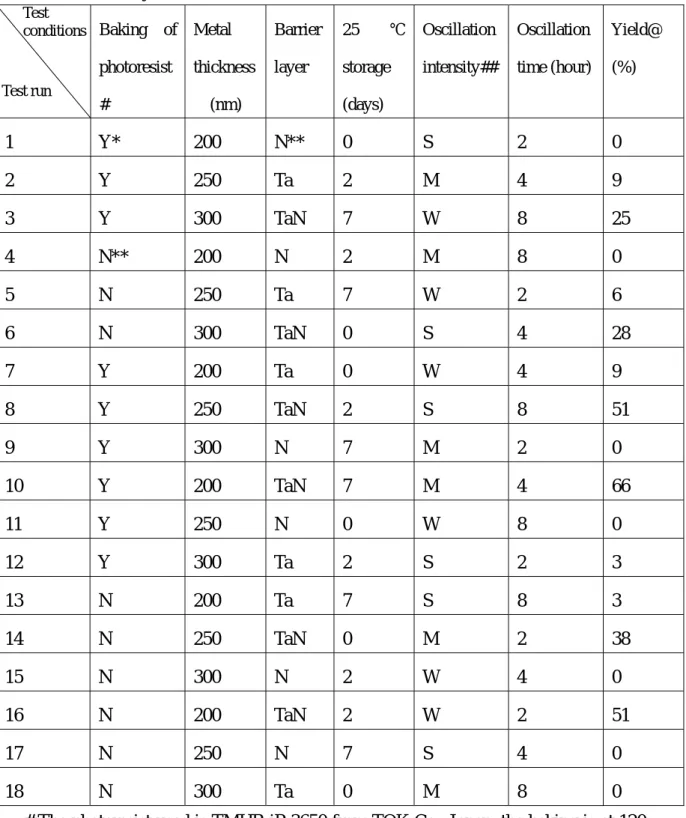
Fig.3 shows the photograph of the patterned interdigitated structure. A summary of the lift-off test designed with Taguchi method is given in Table 1. Among the parameters studied, employment of barrier layer appears to be a key factor to ensure successful lift-off. Barrier layer enhances the adhesion strength of metal to the dielectric and helps in maintaining the pattern integrity during lift-off. The adhesion strength of Cu to SiO2 increases from 9.8MPa to 37.5MPa when a barrier layer is
inserted. On the basis of the yield data shown in Table 1, the optimum Cu lift-off conditions are: curing the photoresist at 120°C for 3 min; a metal thickness of 200nm with 30nm TaN barrier layer, and the ultrasonic oscillation used to strip resist and lift off metal should be medium for an appropriate period of time (4hrs in this study).
The joule heating induced by power consumption will raise the temperature of interconnect and IC chips. The average temperature increase △T in Cu interconnect due to joule heating is shown in Fig.4. The △T of Cu passivated with SiLK (Cu-SiLK) is larger than that of Cu passivated with SiO2 (Cu-SiO2) especially at
Serpentine comb2
Comb1 Serpentine
(a)
Growth of SiO
2(~500nm)
Photolithography to
obtain oxide trenches
Sputtering of metal
(Ta(~30nm) followed by
Cu(~600nm))
Vacuum annealing (60
min at 450℃)
CMP to obtain a smooth
surface
Coating of SiLK or SiO
2Lithography to open bond
pads
Electrical Measurement
Overlayer
deposition
Yes
No
SiO
2Si substrate
Cu/Ta
Cu/Ta
Cu/Ta
Cu/Ta
Air or SiLK or SiO
2(b)
Fig.2(a)Flow chart for the preparation of samples and (b)schematic diagram of the sample cross-section.
Table 1 Summary of the lift-off test Baking of photoresist # Metal thickness (nm) Barrier layer 25 ℃ storage (days) Oscillation intensity## Oscillation time (hour) Yield@ (%) 1 Y* 200 N** 0 S 2 0 2 Y 250 Ta 2 M 4 9 3 Y 300 TaN 7 W 8 25 4 N** 200 N 2 M 8 0 5 N 250 Ta 7 W 2 6 6 N 300 TaN 0 S 4 28 7 Y 200 Ta 0 W 4 9 8 Y 250 TaN 2 S 8 51 9 Y 300 N 7 M 2 0 10 Y 200 TaN 7 M 4 66 11 Y 250 N 0 W 8 0 12 Y 300 Ta 2 S 2 3 13 N 200 Ta 7 S 8 3 14 N 250 TaN 0 M 2 38 15 N 300 N 2 W 4 0 16 N 200 TaN 2 W 2 51 17 N 250 N 7 S 4 0 18 N 300 Ta 0 M 8 0
# The photoresist used is TMHR iP-3650 from TOK Co., Japan, the baking is at 120 ℃ for 3 min, ## ultrasonic oscillation to lift the photoresist off. S: strong (~200Watt), M: medium (~170Watt), W: weak (~140Watt), * y: with baking, ** N: without baking or barrier layer, @: sample size: 65
Test run Test conditions
measuring the temperature coefficient of resistance (TCR)[6]: ) ( ) ( 2 1 2 1 T T R R R T TCR T × − − = (2)
where R1, R2, and RT are the resistance at temperatures T1, T2, and T (T is normally
taken as 20°C), respectively. Therefore, the average temperature rise in the interconnect is : T R T TCR R R T T T × − = − = ∆ ) ( 2 1 2 1 (3)
The TCR’s of Cu-SiO2 and Cu-SiLK are 3.22x10⁻³°C-1 and 3.21x10⁻³°C-1, respectively.
The therml conductivity of SiLK (1.9x10⁻³W/cm-°C) is one eleventh of that of silicon dioxide (2.09x10⁻²W/cm-°C)[3]. The temperature rise induced by the joule heating is dissipated both through the underlayer insulator dielectric to the Si substrate that acts as a heat sink and through the overlayer passivation dielectric, as shown schematically in Fig.5.
The difference in △T between Cu-SiLK and Cu-SiO2 is not very significant. At
a current density of 3x10⁶ A/cm2, △T for Cu-SiLK and Cu-SiO2 are 3°C and 2°C,
respectively, as shown in Fig.4. This suggests that most heat dissipated through the underlayer dielectric to the Si heat sink (substrate), hence, although thermal conductivity of SiLK and SiO2 differs by an order of magnitude, no much difference
is observed between the temperature rise △T of Cu passivated with SiLK and that of Cu passivated with SiO2. Previous work indicates that when using an underlayer
dielectric with poor thermal conductivity, the joule heating could cause a huge temperature rise at interconnects and, hence, accelerates the electromigration damage and finally leads to the catastrophic interconnect failure as well as the thermal decomposition of the underlayer dielectric [7]. The thermal impedance, θj, is defined
by the expression [8]:
△ T=P * θj (4)
where P is the power input of the interconnect. The θj of Cu-SiLK specimen is 1832
℃/W which is 14% higher than that of Cu-SiO2 (1604℃/W), as shown in Fig.6. As
one compares the thermal impedances obtained in this study to those of a previous work which studied the effect of underlayer dielectric on the thermal characteristics of interconnect [7], it is concluded that the thermal conductivity of the underlayer dielectric plays a crucial role in heat dissipation because most heat dissipated through the underlayer dielectric to the Si substrate which has a larger thermal conductivity (6.28*10-1W/cm℃) as compared to the dielectric. In the previous work, polyimide and SiO2 were used as underlayer dielectric. The thermal conductivity of SiO2 is
about twenty times of that of polyimide (1.05*10-3W/cm℃). The thermal impedance of Cu on SiO2 and Cu on polyimide are 234℃/W and 736℃/W, respectively, as
Fig.4 The average temperature increments of Cu interconnect as a function of current density. Ambient temperature: 30℃.
■: Cu passivated with SiO2, ▲: Cu passivated with SiLK
-1 0 1 2 3 4 5 6 7 8 0 5 10 15 20 25
Current density (MA/cm
2)
△T(℃)
Ta
Ta
Fig.5 Schematic diagram for interconnect heat dissipation.
Si substrate
CuOverlayer dielectric
Underlayer dielectric
RSi-a RSi RCu-U RCu-O RO-a TCu0.000 0.002 0.004 0.006 0.008 0.010 0.012 0.014 0 5 10 15 20 25
Power(W)
θ
Cu-SiO2=1604
0C/W
θ
Cu-SiLK=1832
0C/W
Fig.6 Temperature increment versus input power of Cu interconnects with SiO2 or
SiLK passivation.
compared to 1604℃/W (Cu- SiO2) and 1832℃/W (Cu-SiLK) in this study. Besides, a
temperature raise (△T) of over than 600℃ was observed in the Cu on polyimide system and caused the decomposition of the polyimide underlayer. While in this study, the difference in △ T between Cu with different passivation layers is not as significant as that with different underlayers and the magnitude of △T (i.e., 3℃
(Cu-SiLK) and 2 ℃ (Cu- SiO2)) is small. Hence, the thermal conductivity of
passivation dielectric is not as crucial as that of underlayer dielectric in the respect of degradation induced by thermal stress.
The relative resistance R/R0 as a function of time at various temperatures is
exhibited in Fig.7. The resistance increases more rapidly at higher soaking temperature. By defining a resistance change of 4.5% as the criterion of early stage failure, i.e, assuming the dimensions of the maximum voids are much less than the line width, the time rate change of electrical resistance dR/dt due to electromigration damage is thermally activated and can be expressed by the following empirical equation [9]: ] exp[ 1 0 kT Q AJ R dt dR× = n − (5)
where R0 is the initial resistance at a given temperature, A is a preexponential factor,
Jn is the electron current density raised to the n-th power, T is temperature and Q is the activation energy for EM. The activation energy can be obtained from the ln[(dR/dt)(1/R0) versus 1/T plot shown in Fig.8. As can be seen from Figs.7 and 8,
both the time to failure and activation energy for EM of Cu-SiLK are smaller than
those of Cu-SiO2. There are several possible causes which result in shorter EM
lifetime and smaller activation for EM of Cu-SILK as compared to Cu- SiO2. One is
the smaller thermal conductivity of SiLK which causes a larger temperature gradient and accelerates the EM process.
The residual stress of Cu film resulted from the thermal expansion mismatch between the copper and the passivation layer could also affect the EM process, the residual stress can be estimated as follows:
σ=E(αp-αCu)(T-T0) (6)
where E is the Young’s modulus of Cu film(11252kg/mm2), αp and αCu are the
coefficients of thermal expansion (CTE) of passivation layer and Cu, respectively. To
is the annealing temperature (450°C), and T is testing temperature (225°C to 300°C). The CTE of Cu, SiLK, and SiO2 are 16.5, 66, and 0.5ppm/°C, respectively [3,10].
Hence SiLK exerts a compressive stress of 83.54~125.32 kg/mm2 (300°C~225°C),
while SiO2 a tensile stress (27.01~40.51kg/mm2) (300°C~225°C). Previous works
suggests that the presence of high compressive stress would enhance electromigration resistance [11,12]. However, in this study, samples passivated with SiLK (presumably
Fig.7 Relative resistance as a function of current stressing time at various temperatures of Cu passivated with (a) SiO2 and (b)SiLK. Current density:
2.8x10⁶A/cm2 0.999 1.0021.03 1.04 1.05 R0 /R 0.999 1.0021.03 1.04 1.05 R0 /R 0.999 1.0021.03 1.04 1.05 R0 /R 0.999 1.0021.03 1.04 1.05
300
0C
275
0C
250
0C
225
0C
R0 /R 0.999 1.002 1.03 1.04 1.05 R/R 0 3000C 2750C 2500C 2250C 0.999 1.002 1.03 1.04 1.05 R/R 0 0.999 1.002 1.03 1.04 1.05 R/ R0 0.999 1.0021.03 1.04 1.05 R/R 0Fig.8 ln[(dR/dt)(1/R0)] vs. 1/T and activation energy Q for Cu films passivated with
SiO2 (■) or SiLK (▲) during EM test. Current density: 2.8x10⁶A/cm2.
1.70 1.75 1.80 1.85 1.90 1.95 2.00 2.05 -7.0 -6.5 -6.0 -5.5 -5.0 -4.5 -4.0 -3.5 -3.0 -2.5
Q=0.71eV
Q=0.89eV
ln(dR/dt*R
0) (1/ho
u
r)
1000/T (1/
0k)
under compression) have shorter lifetime than those passivated with SiO2 (presumably
under tension). Similar phenomenon was observed on Cu passivated with various polyimide films [13]. It is probably due to the viscoelastic behavior of polyimide and/or that at the testing temperature, the polymer flexes and relieves some of the stress present in a test line. Hence, the effect of the compressive stress on the EM resistance is not appreciable.
Table 2 summarized the failure time and failure time ratio of Cu films stressed at 2.8x10⁶A/cm2 and various temperatures. The ratio of the failure time (tSiLK/tSiO2)
between Cu passivated with SiLK (tSiLK) and Cu passivated with SiO2 (tSiO2) decreases
as temperature increases. The atomic diffusivity D of copper for passivated samples can be expressed as follows [14,15]:
D=D0 exp(-Q/kt)=D0 exp[-(Em+fΩ)/kT] (7)
where f is the constrain force provided by passivation, Ω is the atomic volume, and Em is the activation energy for diffusion. The Young’s modulus of SiO2 and SiLK are
72GPa and 2.45GPa, respectively[3]. The more rigid SiO2 exerts a larger constrain
force on the metallization and retards the diffusion of the metal atoms. Hence, the lifetime for SiO2 passivated samples is longer than that of SiLK passivated ones.
Besides, it is argued that at higher temperatures the polymer relaxes more, the constrain force decreases diffusion of Cu is faster, and consequently, the tSiLK/ tSiO2
ratio decreases with the increase of temperature.
As described in the Experimental Procedure, the out-of-plane dielectric constant (k⊥) is measured with an MIM parallel-plate capacitor structure. The k⊥ of SiLK and
SiO2 are 2.65 and 4.2, respectively. Interdigitated electrode structure, shown in Fig.1,
has been used to determine the in-plane dielectric constant (k//) [1,2]. In order to
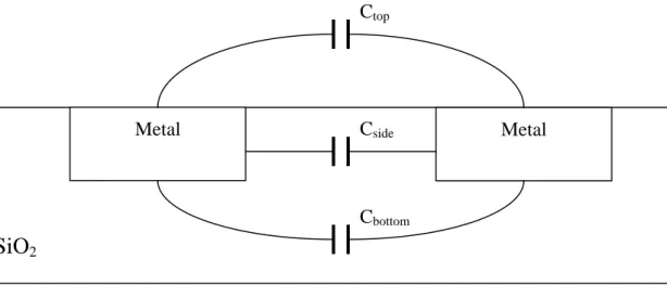
characterize the dielectric properties of SiLK in a structure of its actual use, a multilayer test structure as fabricated as shown schematically in Fig.2. The capacitances between the metal line passivated with air (i.e., without passivation), SiO2, or SiLK are measured. The interdigitated metal line structure is used to amplify
the capacitance between the metal lines, as shown in Fig.2(b). The length of the serpentine metal line is about 400μm. The capacitance measured, C, includes the capacitance contributed by SiO2 (Cbottom + Cside) and the dielectric passivation (Ctop).
As shown schematically in Fig.9(a), C equals to the sum of Ctop, Cside and Cbottom ,
where Cside is the line-to-line capacitance and Ctop and Cbottom are the fringe
capacitance. The capacitance of specimens passivated with air (i.e., unpassivated), SiO2, and SiLK are 0.0226 nF, 0.0369 nF, and 0.0302 nF, respectively. The accuracy
of measurements is ±0.0001nF. The dielectric constant of air is ~1. Because SiO2 is
amorphous and without preferred orientation, the dielectric behavior of SiO2 should
Table 2. Failure time and failure time ratio of Cu films stressed at 2.8x10⁶A/cm2 and various temperatures
Temperature(℃) t*SiO2(x105s) t*SiLK(x105s) tSiLK/ tSiO2
225 5.59 4.18 0.75
250 3.10 2.09 0.67
275 1.58 1.05 0.66
300 0.54 0.29 0.54
* tSiO2 and tSiLK are time to failure for Cu films passivatived with SiO2 and SiLK,
passivation
Fig. 9 (a)Schematic diagram of the capacitance between metal lines and (b)Capacitance vs. dielectric constant plot for specimens with various passivations. The measured capacitance is C, C=Ctop+Cside+Cbottom, and
(Cside+Cbottom) is constant, so the dielectric constant of SiLK can be obtained
the C-k plot. Metal Metal
SiO
2Si substrate
0.5 1.0 1.5 2.0 2.5 3.0 3.5 4.0 4.5 Air SiLK SiO 2 C(nF) k 0.025 0.030 0.035 0.040 0.045 0.050 measurement simulation Ctop Cside CbottomC=Ctop+Cside+Cbottom
(a)
(b)
(Cbottom+ Cside)
structure. Because (Cbottom + Cside) are approximately constant for the three specimens,
the dielectric constant of SiLK can be interpolatd from the C-k curve shown in Fig.9(b). The dielectric constant k thus obtained is 2.701 from SiLK. The k⊥ of SiLK
is 2.65. The difference between the k⊥ and the k obtained from Ctop of Fig.9(a)
suggests that the dielectric behavior of SiLK is anisotropic. The capacitance Ctop
consists of relatively large fringe capacitance from the extension of electric fields around the metal lines. It is beyond the scope of this research to analyze the electric field distribution inside the dielectric layer of the capacitor Ctop and to calculate the
in-plane dielectric constant k// of SiLK on the basis of the gross dielectric constant k
(2.701), the out-of-plane dielectric constant k⊥ (2.65) and the electric field. So it is
assumed that the gross dielectric constant k is the average of k⊥ and k//. The k// thus
obtained is 2.752.
The dielectric anisotropy is attributed to the preferred chain orientation in the plane of the polymeric thin film, resulting in properties in the film thickness direction different from those in the film plane. Cho et.al reported that molecular structure affected the dielectric anisotropy of polymers. Rigid rod-like polymers, such as fluorinated polyimide, EPI-136M, have a strong propensity to align parallel to the substrate when solution cast due to a substrate confinement effect, while flexible chain polymers, such as fluorinated poly(aryl ethyl) (FLARE-1.51), have a smaller propensity to align parallel to the substrate and are more likely isotropic [1]. Table 3 summarizes the chemical structure and the dielectric constant of four low k polymers. Fig.10 exhibits the percent anisotropy ((k// - k⊥)/ k⊥×100%) as a function of weight
and/or length of the monomer. The anisotropy data shown in Table 3 and Fig.10 are derived from three separate studies with three different structures of multilayer test vehicles (references 1 and 2 and this work). Polymers with low monomer weight (<400 g/mole) exhibit small anisotropy, but no specific trend is observed between the anisotropy and weight of monomer, probably due to the experimental errors and/or structural differences. However, the anisotropy increases with further increase of monomer weight, the higher the weight of monomer, the larger the dielectric anisotropy, as can be observed from Table 3 and Fig.10. Factors that affect the evaluation of the in-plane dielectric constant and the anisotropy includes: measurement error (<0.5% in this study), the assumption that the gross dielectric constant is the average of k// and k⊥, structure of the test vehicles, such as: aspect ratio
between the electrode spacing and the dielectric thickness, the hierarchy of the various dielectric layers with respect to metallization, the dependence of the lateral capacitance on the thickness of the dielectric between metal trenches, etc.
Fig.10 Percent anisotropy (k//- k⊥)/ k⊥×100% as a function of (a) length of monomer
and (b) weight of monomer of four low k polymers.
(a)
0.25 0.30 0.35 0.40 0.45 0.50 0.55 0.60 0 5 10 15 20 25FLARE-1.5 [1]
SiLK
BPDA-PDA[1]
EPI-136M [1]
% Anisotropy
Length of monomer, nm.
200 400 600 800 1000 0 5 10 15 20 25EPI-136M[1]
SiLK
FLARE-1.5 [1]
BPDA-PDA[1]
% Anisotropy
Weight of monomer (g/mole)
(b)
because it contains charge carriers that can be displaced (i.e., polarized), and charge displacements within the dielectric can neutralize a part of the applied field, and, consequently, increase the amount of charge stored. There are various possible mechanisms for polarization in a dielectric material, such as: electronic polarization, atomic polarization, molecular (orientation) polarization, and space charge polarization. The dielectric anisotropy of the polymer is resulted from the molecular polarization which has a relaxation time corresponding to the particular material system and, in general, can not follow the electric field when the applied frequency exceeds ~1010Hz.
The leakage current between SiLK and SiO2 is evaluated with the comb and
serpentine interdigitated structure shown in Fig.1. The metal lines were coated with SiLK or SiO2 as described in the experimental procedures. Fig.11 exhibits the comb
current Icomb as a function of serpentine voltage Verp for specimens with different
coatings. It is obvious that the leakage currents of specimens with SiLK overlayer are larger than those of specimens with SiO2 overlayer. There are various paths for
current to flow, such as: through the interface of the overlayer and the underlayer, through the bulk of overlayer, and/or through the underlayer, as shown schematically in Fig.12(a). If the majority current flows through the bulk, the leakage current should be approximately inversely proportional to the length of the path, since the resistance is proportional to the length. As shown schematically in Fig.12(b), Iserp should be
approximately twice of Icomb2. However, if interface current flow dominates, then
there is not apparent relation between leakage current and path length. To identify the major current leakage path, voltage was applied onto pad of comb1 , and currents were measured at pads of comb2 and serpentine. As observed in Fig.13, Iserp is much
larger than Icomb2, this suggests that the SiLK/SiO2 interface is the major path for
current leakage flow.
Table 4 gives a comparison between Cu-SiLKTM and Cu-SiO2 systems. The low
dielectric constant of SiLK renders it a good candidate as interlevel dielectric, however, the larger leakage current, higher thermal impedance and the poor electromigration resistance of Cu passivated with SiLK cast the reliability concerns for Cu-SiLK system.
6.Conclusions
The employment of barrier layer appears to be a key factor to ensure a successful lift-off for Cu interconnects, as the barrier enhances the adhesion strength of metal to the dielectric and helps in maintaining the pattern integrity during lift-off. The thermal impedance of Cu interconnects passivated with SiLK (Cu-SiLK) is about 14% higher
Fig.11 Icomb as a function of Vserp for specimens coated with SiO2 or SiLK 0 2 4 6 8 10 0 200 400 600 800
I
co m b(pA
)
V
serp(V)
SiO
2SiLK
SiO2 or SiLK
Fig.12 (a)Partial cross-section of the specimen and possible current leakage paths indicated by arrows. Current can flow through the overlayer (1,2), the interface between the overlayer and the underlayer (3,4), and the underlayer (5,6). That is Iserp=I(1)+ I(3)+ I(5),
and Icomb2= I(2)+ I(4)+ I(6). (b)Equivalent circuit model when current flown through
bulk layer is the major path. That is Iserp»I(1)+ I(5), and Icomb2» I(2)+ I(6). Ri represents the resistance to current flow via path i and is proportional to the length of the path. Because the distance between comb1 and comb2 is about twice that between comb1 and serpentine, so I(1)»2I(2), I(5)»2I(6), and Iserp»2Icomb2 , if current flown through bulk
is the major leakage path.
comb1 serpentine comb2
(5) (3)
SiO
2Si substrate
(4) (2) (6) comb2SiO
2Si substrate
SiO
2or SiLK
C2 R2 C1 R1 C5 R5 C6 R6 I(2) I(1) I(6) comb1 serpentine I(5)(a)
(b)
(1)Fig.13 Leakage current Iserp and Icomb2 as a function of Vcomb1 for specimens coated with SiLK. 0 2 4 6 8 10 0 200 400 600 800
leakage current (pA)
V
comb1(V)
I
serp
Table 4.Dielectric properties of SiLK and SiO2 as well as reliability issues [16] for
Cu-SiLK and Cu-SiO2 system.
SiLK SiO2 k// 2.752 4.2 Dielectric constant k⊥ 2.65 4.2 % dielectric anisotropy (k//- k ⊥)/ k⊥×100% 3.85 0 Dielectric leakage current Icomb at Vserp=6V, (pA)(Fig.11) 568 112
For reliability issues[16] Cu-passivated
with SiLK
Cu-passivated with SiO2
Thermal impedance of Cu, °C/W 1832 1604
225℃ 4.2×10⁵s 5.6×10⁵s 250℃ 2.1×10⁵s 3.1×10⁵s Electromigration (EM) lifetime of Cu interconnects at 2.8×10⁶A/cm2 300℃ 2.9×10⁴s 5.4×10⁴s
Activation energy Q for EM
of Cu (eV.) 0.71 0.89 100℃ 6.49×10⁷s 8.51×10⁸s Predicted EM lifetime* of Cu interconnect at 2.8×10⁶A/cm2 25℃ 1.69×10 10 s 9.04×10¹¹s
* The predicted EM lifetime is calculated on the basis of Ahhrenius
equation:
exp(
)
2 1 2 1kT
Q
kT
Q
t
t
T T=
−
than that of Cu passivated with SiO2 (Cu- SiO2). Besides, the difference in joule
heating induced temperature increase △T between Cu-SiLK and Cu-SiO2 is not
significant. This suggests that most heat dissipated through the underlayer dielectric to Si substrate which acts as a heat sink. Hence, the thermal conductivity of passivation dielectric is not as critical as that of underlayer dielectric in the respect of thermal stress induced degradation. The electromigration resistance and lifetime of SiLK passivated Cu is poorer than those of SiO2 passivated one. This is attributed to the
small thermal conductivity and low rigidity of SiLK dielectric.
The dielectric anisotropy of SiLK films is studied. The out-of-plane dielectric constant (k⊥), measured with an MIM structure, is 2.65. The in-plane dielectric
constant (k//) was evaluated with a comb and serpentine interdigitated structure and an
assumption of equal contribution of k⊥ and k// to the gross dielectric constant. The k//
obtained is 2.752. The dielectric anisotropy of SiLK, ~3.85% is attributed to the molecular polarization and should fade away at high frequencies (>1010Hz). The low dielectric constant renders SiLK a good candidate to replace SiO2 for interlevel
dielectric. However, Cu passivated with SiLK exhibits larger leakage current, higher thermal impedance, and shorter electromigration lifetime than that passivated with SiO2. Hence, there is a reliability concern for the integration of Cu-SiLK system.
7.成果自評
本計畫原申請為三年期,但核定為兩年期,因此研究進度及項目皆作調整, 已在兩年內完成原訂三年的工作,本計畫第一年的研究成果已寫成精簡報告於 92 年 5 月 26 日繳交,是以該部分成果並未涵蓋在此份報告中。
本計畫之研究成果已整理成兩篇論文,一篇已發表於國際期刊(Electromigration and Integration Aspects for Copper-SiLKTM System, Journal of Electronic Materials, 33(2004)796) , 另 外 一 篇 送 審 中 (Dielectric Anisotropy in the Integration of
Cu-SiLKTM System)。
8.參考文獻
1.T.H.Cho, J.K.Lee, P.S.Ho, E.T.Ryan, and J.G.Pellerin, J.Vac. Sci. Tecnol., B18(2000)208.
2.A. Deutsch, M. Swaminathan , M.-H.Ree, C.Surovic, G.Arjavalingam, K.Prasad, D.C.McHerron, M.McAllister, G.V.Kopcsay, A.P.Giri, E.Perfecto, and G.E.White, Proceedings, the Topical Meeting on Electrical Performance of Electronic Packaging, Monterey, California, pp.151-154, 1993
3.S.J.Martin, J.P.Godschalx, M.E.Mills, E.O.Shaffer Ⅱ, and P.H.Townsend, Adv. Mater., 23(2000)1769.
H.Feldis, R.Blanc, E.Tabouret, D.Louis, C.Arvet, E.Lajoinie, Y.Gobil, G.Passemard, F.Jourdan, M.Moussavi, M.Cordeau, T.Morel, T.Mourier, L.Ulmer, E. Sicurani, F.Tardif, A.Beverina, Y.Trouillet, and D.Renaud, Proceeding, International Interconnect Technology Conference, p.198, 1999.
5.J.D.Plummer, M.Deal, and P.B.Griffin, “Silicon VLSI Technology: Fundamentals, Practice and Modeling”, Prentice Hall, p.58, 2000.
6.H.Shafft and J.A.Lechner, “Statistics for Electromigration Test”, IRPS, pp.192-202, 1988.
7.Y.L.Chin, and B.S.Chiou, Jpn. J. Appl. Phys., (in press).
8.K.Banerjee, A.Amerasekera, G.Dixit and C.Hu, Proc. IEDM, pp.65-68, 1996. 9.C.K.Hu, B.Luther, F.B.Kaufman, J.Hummel, C.Uzoh, and D.J.Rerson, Thin Solid
Films, 262(1995)84.
10.S.P.Murarka: Metallization Theory and Practice for VLSI and ULSI (Butterworth-Heinemann, New York, 1993) p.69.
11.J.R.Lloyd, Thin Solid Films, 91(1982)175.
12.J.R.Lloyd, and P.M.Smith, J. Vac. Sci. Tech., A1(1983)455.
13.J.S.Jiang, and B.S.Chiou, Intl. J. Microcircuits and Electronic Packaging, 22(1999)395.
14.I.A.Blech, J.Appl. Phys., 47(1976)1203.
15.J.R.Lloyd, Mater. Res. Symp. Proc., 428(1996)3.
16.H.S.Tseng, B.S.Chiou, W.F.Wu, and C.C.Ho, “Electromigration and Integration Aspects for Copper-SiLKTM Syetems”, J.Electronic Materials, 33(2004)796.
![Table 4.Dielectric properties of SiLK and SiO 2 as well as reliability issues [16] for Cu-SiLK and Cu-SiO 2 system](https://thumb-ap.123doks.com/thumbv2/9libinfo/8747370.205223/27.892.162.727.181.880/table-dielectric-properties-silk-sio-reliability-issues-silk.webp)
