國
立
交
通
大
學
電子工程學系電子研究所
博 士 論 文
非對稱輕摻雜汲極金氧化半導體電晶體微波電性分析
Radio Frequency Performance of Asymmetric- Lightly-Doped-Drain
Metal-Oxide-Semiconductor Field-Effect Transistors
研 究 生:張 慈
指導教授:荊鳳德 教授
非對稱輕摻雜汲極金氧化半導體電晶體微波電性分析
Radio Frequency Performance of Asymmetric- Lightly-Doped-Drain
Metal-Oxide-Semiconductor Field-Effect Transistors
研 究 生:張 慈 Student:Tsu Chang
指導教授:荊鳳德 博士 Advisor:Dr. Albert Chin
國 立 交 通 大 學
電子工程學系電子研究所
博 士 論 文
A Dissertation
Submitted to Department of Electronics Engineering and Institute of Electronics
College of Electrical and Computer Engineering National Chiao Tung University
in partial Fulfillment of the Requirements for the Degree of
Doctor of Philosophy in
Electronics Engineering
January 2010
非對稱輕摻雜汲極金氧化半導體電晶體微波電性分析
研究生 : 張慈 指導教授 : 荊鳳德 教授
國立交通大學電子工程系電子研究所
摘要
在這論文中報告 0.18 微米非對稱輕摻雜汲極功率金氧化半導體電晶體特性 的設計,這類型元件不具備n型汲極伸展區,使用台積電代工一層多晶矽六層金 屬標準製程,而不會需要改變任何製程參數,在相同的閘極寬度下比傳統金氧化 半導體電晶體有較佳的特性。該元件具有直流崩潰電壓 6.9 V,功率密度 0.54 W/mm,最大振盪頻率 115 GHz,較佳的相鄰通道功率抑制線性度特性,在 2.4 GHz 有優異之汲級效率 52 % 。進而分析模型化了 0.18 微米非對稱輕摻雜汲 極金氧化半導體電晶體的射頻功率特性,使用校正後之元件模型與直流電壓電流 量測,雜散參數與射頻功率資料相對應,建立非對稱輕摻雜汲極功率金氧化半導 體電晶體模型以製作之兩級放大器晶片之製作,具有晶片電感電容元件匹配,在 增加偏壓,所量測之功率輸出增加,該晶片在 2.4 GHz 具有良好之功率特性,具 有 19.6 dB 功率增益,較高之 23.3 dBm 輸出功率, 29.6 % 功率附加效益,在 18 dBm 輸出時具有優異之 -36 dBc 相鄰通道功率抑制線性度之特性,晶片面積 僅1-mmx1.1-mm。 另外選用總寬度為 200 微米非對稱輕摻雜汲極功率金氧化半導體電晶體功率元件,利用基板磨薄技術使得矽基板僅餘 50 微米,矽基板轉移至碳化矽成為 散熱基板使用,使得非對稱輕摻雜汲極金氧化半導體電晶體於碳化矽上得到DC 及RF效能提昇近 6.6 % ,碳化矽具備比矽材料高三倍之高導熱係數,且具有高 基板阻值的特性,使得該大尺寸之 50 微米矽基板非對稱輕摻雜汲極功率金氧化 半導體減少了自我加熱及基板的雜散效應,因此,50 微米矽基板轉換於碳化矽 之非對稱輕摻雜汲極功率金氧化半導體之功率增益、飽和輸出功率及功率附加效 益等參數得以提昇。
Radio Frequency Performance of Asymmetric-
Lightly-Doped-Drain Metal-Oxide-Semiconductor
Field-Effect Transistors
Student: Tsu Chang Advisor: Prof. Albert Chin
Department of Electronics Engineering & Institute of Electronics
National Chiao-Tung University
Abstraction
We report the performance of 0.18 μm RF power MOSFETs with an
Asymmetric-Lightly-Doped-Drain (LDD) design. Such devices do not have an n+ drain extension using a foundry-standard 1P6M process, without making any process modifications and exhibited better characteristics than conventional MOSFETs with the same gate length. The devices showed a DC breakdown voltage of 6.9 V, a 0.54 W/mm power density, 115 GHz fmax, and a good adjacent channel power ratio (ACPR)
linearity, as well as a 52 % drain efficiency at 2.4 GHz .Moreover, we have modeled the RF power performance of 0.18 μm asymmetric-LDD MOSFET. Using the
well-calibrated device model with good matching to measured DC I-V, S-parameters and RF power data, we have fabricated a 2.4 GHz two-stage RF power amplifier using the asymmetric-LDD MOSFET cells and on-chip matching inductors. The measured output power increases with increasing bias voltages. Good RF power
performance was measured at 2.4 GHz with 19.6 dB power gain, large 23.3 dBm output power, high 29.6% PAE, excellent ACPR linearity of -36 dBc at 18 dBm and small die size of only 1-mm×1.1-mm.
In this thesis, the total width 200 μm of asymmetric-LDD MOSFET (AMOSFET)
cells presents the DC characteristics and radio frequency (RF) power performance improvement as high as 6.6% with 50 μm thick silicon substrate on SiC substrate. The self-heating effect and parasitic effect of the large size AMOSFET with 50 μm
thick silicon on SiC substrate is reduced due to good heat dissipation and less lossy of thinned silicon substrate and SiC substrate. Therefore, the power gain, saturation output power and power added efficiency of AMOSFET with 50 μm Si substrates
ACKNOWLEDGMENTS
I would first like to thank my adviser Prof. Albert Chin for his illuminative suggestions and discussions during the period of my working toward PhD degree. His inspiration benefits me a lot on the creative ideas, effective schedule control and the integrity to the processing tasks.
I appreciate the financial and equipment supports from National Science Council, National Nano Device Lab. and Semiconductor Center of NCTU. I am also grateful to those who ever assisted this work: the crews of ED633 Lab and the assistance professor Dr. Hsuan-ling Kao from Dept. of Electronic Engineering, Chang Gung University. And also specially thanks for the supports from all colleagues in Chung-Shan Institute of Science & Technology.
Finally, much gratitude must be expressed to Dept. of Electronics Eng., NCTU, for the 4-year training. The encouragements from my father, mother and my wife Gina who always support and give me all their loves. This work can’t be finished without them.
CONTENTS
ABSTRACT
iACKNOWLEDGMENTS
vCONTENTS
viFIGURE CAPTIONS
ixTABLE CAPTIONS
xiiiCHAPTER
1
Introduction
1
1.1 Motivation
1
1.2 Si RF MOSFETs Technology and Modeling
3
1.3
Innovation
and
Contribution
5
CHAPTER 2 Fundamental of RF Power Amplifier
7
2.1
Introduction
7
2.2 Amplifier parameters
8
2.3 Loadline matching and Load pull measurement
11
CHAPTER 3 RF Power Characteristics of CMOS -
Compatible Asymmetric-LDD MOS
Transistor
18
3.1 Introduction
18
3.2 EXPERIMENTAL PROCEDURE
21
3.3 Device Characteristic of RF AMOSFETs
22
3.3.1 DC and small signal RF characteristics 223.3.2 Device modeling of the AMOSFET 25
3.3.3 RF power performance of the AMOSFET 27
3.3.4. Linearity in saturation 29
3.4 Conclusions
30
CHAPTER 4 A Single Chip Implementation for
2.4GHz Linear Power Amplifier
47
4.1 Introduction
47
4.2 Architecture
49
4.3
Small-signal
characteristics
50
4.4
Large
signal
characteristics
51
4.5 Linearity
52
4.6 Conclusions
53
CHAPTER 5 RF AMOSFETs on SiC Substrate
59
5.2
Experiment
Procedure
61
5.3 DC Characteristic of 0.18
μm RF AMOSFETs on SiC
Substrate 63
5.4 S-parameter of 0.18
μm RF AMOSFETs on SiC
Substrate
64
5.5 RF Power Characteristics
69
5.6 Conclusions
71
CHAPTER 6 Conclusions and Future Work 82
6.1 Conclusions
82
6.2
Future
Works 83
REFERENCES
84VITA
100
FIGURE CAPTIONS
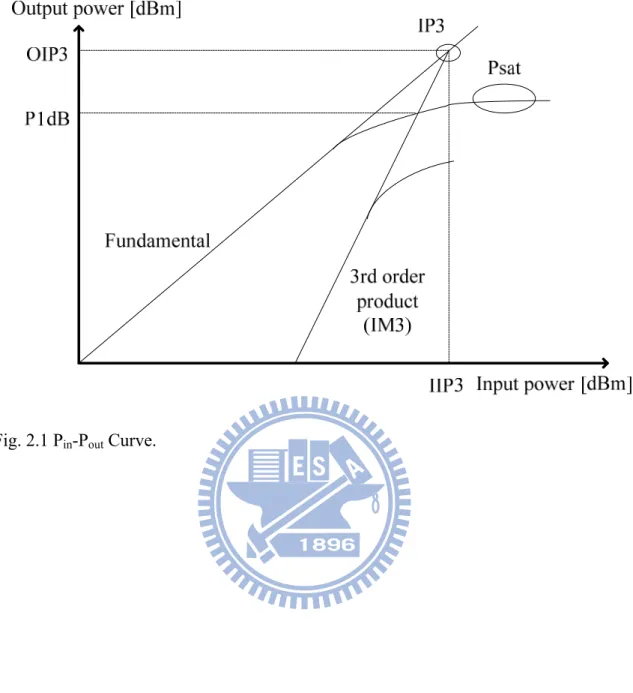
Fig. 2.1 Pin-Pout Curve. 14
Fig. 2.2 Spectrum for a nonlinear RF amplifier. 15 Fig. 2.3 Optimum load is decided by the bias point and I-V characteristics of the
transistor.
16 Fig. 2.4 Typical equipment configurations for Load pull measurement system. 17 Fig. 3.1 The cross-sectional view of an asymmetry-LDD NMOSFET. The
0.18μm gate length, conventional MOSFETs have a wide spacer. 31
Fig. 3.2 (a) The Id-Vd characteristics at Vg of 0 V and (b) Id-Vg characteristics for
conventional and asymmetric-LDD n-MOSFETs with LG=0.18 μm. 32
Fig. 3.3 The electric potential of conventional and asymmetric-LDD 0.18μm RF MOSFETs.
33 Fig. 3.4 Energy band diagram of conventional and asymmetric-LDD devices.
The thick undoped LDD lowers the electric field and increases VBD. 34
Fig. 3.5 Id-Vd and gm-Vg curves for conventional and asymmetric-LDD nMOSFETs with Lg=0.18μm and at Vd=1.8V.
35
Fig. 3.6 Measured and simulated (a) Id-Vd and (b) Id-Vg characteristics for
10-gate-finger conventional and asymmetric-LDD 0.18 μm RF
MOSFETs.
36 Fig. 3.7 Measured (solid symbols) and simulated (line) S-parameters for (a)
conventional and (b) asymmetric-LDD 0.18 μm RF MOSFETs.
37
Fig. 3.8 Measured and simulated |H21|2,Gmax, ft and fmax characteristics for
conventional and asymmetric-LDD 0.18 μm RF MOSFETs. The ft was
obtained by extrapolating |H21|2 to 0 dB with a -10 dB/decade slope. The
fmax was obtained by extrapolating the MAG to 0 dB. 38
Fig. 3.9 The self-consistent device model of asymmetric-LDD 0.18 μm RF MOSFETs to simulate the DC, small signal S-parameters to large signal RF power characteristics. 39 Fig. 3.10 Measured and simulated ft, fmax and gm characteristics of conventional
and asymmetric-LDD 0.18mm RF MOSFETs.
40 Fig. 3.11 Measured and modeled RF output power and PAE at 2.4 GHz for both
types of device. 41 Fig. 3.12 Measured and simulated power density as functions of operation
frequency and Vd bias for conventional and asymmetric-LDD 0.18μm RF
Fig. 3.13 The dependence of the power density on device length. 43
Fig. 3.14 Input and output voltage and current swing of the devices at the 10 dBm RF input power for (a) Conventional (ZS=195+j168.8, ZL=95.1+j20.9), (b) asymmetrical-LDD at Vd=2.5V (ZS=195+j168.8, ZL=121.2+j29.8) and (c) at Vd=3.0V (ZS=195+j168.8, ZL=120.5+j40) 0.18 μm RF MOSFETs. 44
Fig. 3.15 ACPR vs. output power of conventional and asymmetric-LDD 0.18μm RF MOSFETs @ 2.4 GHz. 45
Fig.4.1 A schematic of the 2-stage MOS PA
54
Fig.4.2 Measured and simulated gain and return loss for MOS PA.
55
Fig.4.3 Measured and simulated RF output power, gain and PAE.
56
Fig.4.4 Measured ACPR of the MOS PA.
57
Fig.4.5 An image of the PA chip with 1-mm×1.1-mm die size. 58
Fig. 5.1 (a) Image of a 50 μm thick die on SiC substrate. (b) The substrate thickness measurement after thinned-down procedure. 72
Fig. 5.2 The drive current of 0.18 μm AMOSFETs on VLSI-standard Si substrate and 50 μm Si substrate on SiC.
73
Fig. 5.3 The increasing rate of the drain current for 0.18 μm AMOSFETs on VLSI-standard Si substrate and 50 μm Si substrate on SiC at Vd = 1.8 V.
74
Fig. 5.4 The DC transconductance gm of 0.18 μm AMOSFETs on VLSI-standard
Si substrate and 50 μm Si substrate on SiC. 75
Fig. 5.5 Measured ⎪H21⎪2 and Gmax characteristics of 0.18 μm AMOSFETs on
VLSI-standard Si substrate and 50 μm Si substrate on SiC.
76
Fig. 5.6 The equivalent circuit model of NMOSFET, the elements in dotted box are the intrinsic elements.
77 Fig. 5.7 Measured (solid symbols) and simulated (line) S-parameters for (a) no thinned-down and (b) thinned-down of asymmetric-LDD 0.18 μm RF
MOSFETs.
78 Fig. 5.8 The equivalent circuit model of NMOSFET for Vgs<Vth. 79
Fig. 5.9 Measured RF output power, gain and PAE of 0.18 μm AMOSFETs on VLSI-standard Si substrate and 50 μm Si substrate on SiC at 2.4 GHz.
TABLE CAPTIONS
Table.3.1 Comparison of LDMOS, Conventional and Asymmetric MOSFETs(*Calculate from P1dB; **4dB compression). 46
Table.5.1 Comparison of gm and Rsub for 0.18 μm AMOSFETs on VLSI-standard
Chapter 1
Introduction
1.1 Motivation
Fundamental challenges of Si-based RF technology include the poor power performance of the devices and the loss in associated passive devices such as inductors, transmission lines, and the probing pads [1.1.1]-[1.1.7]. The RF loss in the passive devices can be reduced by using micro-strip lines [1.1.5]-[1.1.7], an etched air-gap, or proton implantation [1.1.1]-[1.1.5]. These approaches help shield the components from the low-resistivity Si substrate. However, little progress has been made in improving the MOSFET RF power performance, even though device scaling has resulted in improvements in the RF gain, the unity-gain cut-off frequency (ft), the maximum
frequency of oscillation (fmax) and the RF noise figure [1.1.8] -[1.1.10]. The poor RF
power output of Si MOSFETs arises from the lower drain breakdown voltage when compared with GaAs FETs. This reflects the smaller bandgap in Si (1.1 eV) compared with that for GaAs (1.42 eV). The drain breakdown voltage also deteriorates with
low cost and high integration capability. To address this challenge, lateral double-diffused MOS (LDMOS) transistors [1.1.11]-[1.1.15] have been proposed to improve the breakdown voltage, by trading-off the on-state resistance (Ron). This requires customized,
complex process steps, and the resulting lower ft and fmax limit the high frequency
operation of applications [1.1.11]-[1.1.15].
Here we report the RF performance of a 0.18μm asymmetric-LDD MOSFET that
has a high drain-breakdown voltage. This device preserves the high RF gain, ft and fmax,
permitting superior high frequency operation. The higher breakdown voltage results from creating a wider drain depletion regime, and is a different approach from that in LDMOS devices. The reported devices are fully-compatible with standard foundry logic processes, being achieved by blocking the n+ ion implantation at the drain extension, using an extra
mask or embedded the design in the p-MOSFET mask. Thus no customized process steps are required.
1.2 Si RF MOSFETs Technology and Modeling
Silicon RF MOSFETs are now widely-used for wireless communications, due to the improvements of the larger RF gain, higher current-gain (|H21|2) cut-off frequency (ft)
and better power-gain (Gmax) maximum oscillation frequency (fmax) with transistor
down-scaling and technology evolution [1.2.1]-[1.2.7]. This has led MOSFETs the prime choice for wireless communication and RF system-on-chip (SoC) application such as WiMAX, W-LAN, and Ultra-Wide Band (UWB). However, one fundamental challenge for MOS transistors is the relative poor RF power performance, which is due to the lower drain breakdown voltage for RF power delivery. The breakdown voltage becomes even worse with down-scaling MOSFET, even though the higher fT and fmax allow a higher
frequency operation with higher gain. Nevertheless, the MOSFET is still desirable for RF power application because of the low cost and very high-density circuit integration. To improve the breakdown voltage, lateral-diffused MOS (LDMOS) transistors [1.2.8] have been proposed. However, the issues are the lower ft and fmax difficult for higher RF
frequency application and the non-standard process with extra process steps and masks beyond IC foundry.
An accurate device model from DC to RF frequency range is necessary to confirm required specification of designed circuit, and to shorten design cycle. The power performance is a principal requirement for RF circuit design, for example: power
amplifier (PA) design. The design of power amplifier not only needs precise DC and S-parameters model but even more needs accurate large signal model to evaluate the power performance of the circuit. It is needed a physical MOSFET model in a specific frequency range capable of simulation of DC to RF characteristics. BSIM3 model is a good candidate for DC modeling and it allows users to accurately model upon parameter extraction on existing technology or predict MOSFET behavior based on the default or an extracted technology. However, when BSIM3 model is applied to simulated S-parameter and power performance of 0.18 μm asymmetric-LDD MOSFET at high frequency, it
must require some modification for fitting both characteristics of the device. In this thesis, we provided a modified BSIM3 model to predict device DC I-V, S-parameters, and Power performance. The precise RF model is important for the implementation of MOSFETs and other device in RF front-end circuit.
1.3 Innovation and Contribution
In this thesis, we first Here we report the RF performance of a 0.18μm
asymmetric-LDD MOSFET that has a high drain-breakdown voltage. This device preserves the high RF gain, ft and fmax, permitting superior high frequency operation. The
higher breakdown voltage results from creating a wider drain depletion regime, and is a different approach from that in LDMOS devices. The reported devices are fully-compatible with standard foundry logic processes, being achieved by blocking the n+ ion implantation at the drain extension, using an extra mask or embedded the design in
the p-MOSFET mask. Thus no customized process steps are required. This approach almost doubles the DC breakdown voltage, to 6.9 V, leading to an increase in the RF voltage swing, and an output power improvement as high as 64% at 2.4 GHz - compared with conventional MOSFETs at the same 0.18 μm gate length. In addition the linearity of
ACPR was 8 dB better, with a high 52% drain efficiency. These results are among the best published data for MOS transistors [1.1.11]-[1.1.15] used in RF power applications.
This thesis also presents the DC characteristics and radio frequency (RF) power performance improvement as high as 6.6 % of asymmetric lightly-doped-drain
metal-oxide-semiconductor field-effect transistors (Asymmetric LDD MOSFET, AMOSFET) with 50 μm thick silicon substrate on SiC substrate. The self-heating effect and parasitic effect of the large size AMOSFET with 50 μm thick silicon on SiC substrate
is reduced due to good heat dissipation and less lossy of thinned silicon substrate and SiC substrate. Therefore, the power gain, saturation output power and power added efficiency of AMOSFET with 50 μm Si substrates mounted on SiC substrate is improved.
Chapter 2
Fundamental of RF Power
Amplifier
2.1 Introduction
The main purpose of this chapter is to introduce the fundamental principles and parameters of power amplifier. In this thesis power amplifiers are based on the MOS devices. And its RF operation as well as device model is extremely important for microwave power amplifier design, which is will be introduced in the Chapter 3.
Power amplifiers can be divided into different classes of operations [2.1.1]. Based on where is biased and if the device is operated as a switch, there are broadband linear amplifiers, (such as Class A, AB, and B), tune power amplifiers (such as Class C and F), switch mode power amplifiers (such as Class D and E). Since the linearity, efficiency and bandwidth are of interest in this work, only the Class A, AB power amplifier will be discuss. In this chapter, Class A configuration is chosen as an example to demonstrate the concept and principle of linear RF power amplifiers design.
2.2 Amplifier parameters
Some important characteristics of power amplifier are listed below [2.2.1].
(1) Output power of PA
Output power which is a function of the input power is from the power deliver to the load. The Psat as refer in the fig. 2.1, define as maximum saturated power. The P1dB is
defined the gain is compressed by 1 dB.
(2) Power gain
The power amplifiers are characterized by transducer power gain defined as the ratio of the power delivered to the load (Po) to the power available from the source (Pin) to the
amplifier. The power gain is defined as
in o
P
P
G
=
/
(3) Efficiency of PA
There are two way to define the efficiency, Drain efficiency or power added efficiency. Drain efficiency can be define as
Drain efficiency=
dc out dsbias bias out P P V I P = *efficiency (PAE), it is more reasonable indication of PA performance, which is a metric for rating the efficiency of a power amplifier that takes into account the effect of the gain of the amplifier. It is calculated as.
Power Added efficiency=
dc out dc in out P P G P P P )* 1 1 ( ) ( − = −
<Drain efficiency
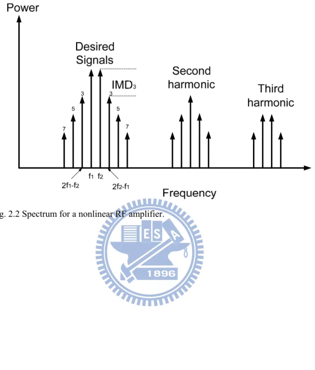
(4) LinearityA real amplifier with nonlinear transfer characteristic, the output signal waveform in general exhibits extra frequency components at the output. The transfer function of a weakly nonlinear system can be written as a Taylor series expansion as below:
.... 4 4 3 3 2 2 1 0+ ⋅ + ⋅ + ⋅ + ⋅ + = in in in in out a a V a V a V a V I
Given an input signal at single frequency f1, the higher order harmonics of 2f1 and 3f1
will be generated.
When two signals f1 and f2 with different frequencies are applied to a nonlinear, not
only the harmonic components of those two frequencies will be generated, but also mf1+nf2 intermodulation products ( IM ), which are closed to f1 and f2, produce distortion
in the output (shown in the Fig. 2.2 ).
The third-order term will be generated 3rd intermodulation products at (2f1-f2) and (2f2-f1) which are call IM3 components. The difference between the IM3
3 3 Vin a ⋅
intermodulation distortion ( IMD3 ) or IM3 suppression, and the linearity performance of
a power amplifier can be described by the IMD3.
The harmonic frequency components created by the nonlinear terms could be removed by an output bandpass filter centered at the fundamental frequency. However, if the frequencies of the two-tone signals are close, the intermodulation products will be close to their fundamental frequency (in-band), therefore cannot be removed by filtering. In wireless communication systems, the band intermodulation signals lie in adjacent channels, which will create interference. Therefore, linearity performance is a very important factor for a RF power amplifier.
Adjacent Channel Power Ratio (ACPR) is a factor of linearity of power amplifier which measured the amount of interference, or power, in the adjacent frequency channel. ACPR is usually defined as the ratio of the average power in the adjacent frequency channel (or offset) to the average power in the transmitted frequency channel. It is a critical measurement for CDMA transmitters and their components. It describes the amount of distortion generated due to nonlinearities in RF components.
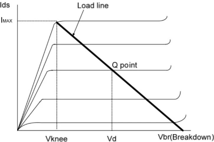
2.3 Loadline matching and Load pull measurement
For power amplifier extract more power from the transistor becomes more important. Therefore, the intrinsic transistor output is matched to an optimum load decided by the bias point and large-signal I-V characteristics of the transistor in order to obtain maximum available output power (as shown in Fig.2.3). The method to get the optimum impedance is the load line theory which is proposed by Cripps [2.3.1]. The optimum load impedance Ropt is defined by
Max knee br opt I V V R = ( − )
where Imax is the maximum current, Vbr is the breakdown voltage and Vknee is the knee
voltage of the active device. The calculated Ropt is the best matching impedance for the
maximum output power. Under this matching condition, the device will deliver an optimum output power is as following equation
8 ) ( br knee Max opt I V V P = − ×
The reactance of device output impedance can be determined by the small signal (S parameter) model. The calculated Gamma output including Ropt and reactance will be the
simple estimated method to get the optimum output power.
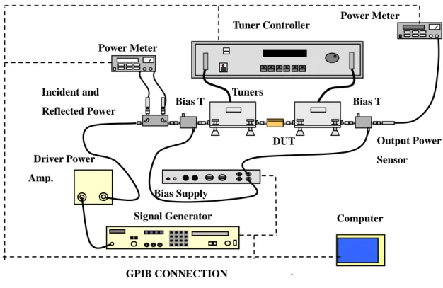
Another method is the load pull measurement which is the key verification method in this thesis. The load pull measurement is one direct large signal measurement
technique to characterize device properties [2.3.2]. The measurement system simultaneously monitors the tuned impedance of the characterization circuitry and the performance of the device. Device response is then recorded under the variable load condition. The optimum load and source impedance will be displayed on a smith chart and obtain the optimum output power and power added efficiency. The load pull contours are determined for one frequency at a time. For wide band characterization, load pull measurements can be taken at several discrete frequencies within the band of interest.
Fig.2.4 shows a typical equipment configuration that can be used to realize a traditional load pull system. A large amplifier signal is supplied to the DUT from the driver amplifier. The input tuner is used to optimize the input match and to assure maximum power transfer to the device. The output tuner is tuned to realize some specific performance. Bias to the device under test is through the bias tees placed in the system. In this thesis, the ATN load pull system was performed to verify the power amplifier characteristics. The advantages of ATN automatic load pull system which tuner is solid state devices are fast and vibration free. However, the mechanical tuner has the superior characteristics of power limitation and high gamma more than the solid state tuner. In the medium power amplifier application, the ATN load pull system is suitable for testing under the stable and fast condition.
amplifiers. Load pull measurements do not provide an easy means for performing parameter extraction of large signal model parameters. However, the data can be used to choose the optimal devices for specific power applications and to verify large signal model.
Fig. 2.3 Optimum load is decided by the bias point and I-V characteristics of the transistor.
Fig. 2.4 Typical equipment configurations for Load pull measurement system. Power Meter Power Meter Bias T Bias T Output Power Sensor Signal Generator Tuner Controller Bias Supply DUT Tuners Incident and Reflected Power GPIB CONNECTION Driver Power Amp. Computer
Chapter 3
RF Power Characteristics of
CMOS - Compatible Asymmetric
-LDD MOS Transistor
3.1
Introduction
PAs are typically the most important building blocks of RF transceivers. PA require large output power with efficiency and linearity to transmit RF signal. It will be a challenge to increase output power, efficiency and linearity at the same time, so that is the reason why discrete or hybrid implementations of this circuit are so popular. Pseudo-morphic High Electronic Mobility Transistor (pHEMT) FET, Hetero-junction bipolar transistor (HBT), bipolar junction transistor (BJT), CMOS, Bi CMOS, LDMOS are common implementation of RF integrated circuit. However, the CMOS PAs have the advantages of the integration of silicon technology. The studies of CMOS PAs are more important in the transmitter system.
The technological evolution and down-scaling of Si MOSFETs have produced continuing improvements in the RF gain, cut-off frequency (ft), maximum oscillation
frequency (fmax) and RF noise figure [3.1.1]-[3.1.5]. However, the down-scaled devices
breakdown voltage. A transistor design, termed Lateral Diffused MOS (LDMOS), has been proposed to improve the RF output power, by increasing the drain breakdown voltage. However, the RF performance of an LDMOS device comes at the expense of a relatively large on-resistance, and low ft and fmax [3.1.6]-[3.1.9]. Additional processing
steps and masks are also needed for LDMOS, when compared with standard CMOS. To address this issue we have previously proposed an asymmetric-lightly-doped-drain (LDD) MOSFET which can increase the drain breakdown voltage and RF output power [3.1.13]. However, it is unclear if the improved RF power performance of such an asymmetric-LDD MOSFET can be further improved at shorter gate lengths with higher operation frequencies. The realization of both the high power density and low ACRP is difficult when scaling the gate length (Lg). Long gate length (Lg) and long drain side
region have been used to improve breakdown voltage (VBD) [3.1.14]. However, the long
gate length degrades gain and the long drain side region increase parasitic resistance and impacts the output power (Pout). In this paper, we further studied the scalability of this
asymmetric-LDD MOSFET [3.1.15] to 0.18 μm which increase VBD and power density
as well as improving linearity of ACPR due to higher bias point. In this thesis, we report on the performance of an asymmetric MOSFET having a 0.18 μm gate length. This
asymmetric-LDD MOSFET has been fabricated within a conventional foundry process. The output power of the asymmetric-LDD MOS transistor has been found to increase by
as much as 64% at 2.4 GHz under saturated power conditions. This performance is better than or comparable with the data of other MOS transistors for high frequency power applications [3.1.6]-[3.1.12] with additional advantage without making any process modifications.
3.2
EXPERIMENTAL PROCEDURE
A foundry standard 0.18 μm 1-poly-6-metals (1P6M) logic process was used in this
study. To increase the breakdown voltage of asymmetric-LDD MOSFET, the drain LDD region was removed by an n+ ion-implantation blocking mask [3.1.13] [3.1.15], as shown
in Fig. 3.1. Conventional MOSFETs were also fabricated for comparison. The p-type region underneath the drain spacer forms a wider depletion region to allow larger applied drain voltage. Multiple gate fingers layout has been used, which have 10-gate-finger in these MOS transistors with 0.18 μm gate length and 5 μm widths. Standard
coplanar-waveguide (CPW) RF layout was used for on-wafer probing [3.1.1]-[3.1.5]. The small signal S-parameters are measured from 45 MHz to 26 GHz by CASCADE probe station and SOLT standard calibration procedure using HP8510C network analyzer. The intrinsic device characteristics were obtained by a de-embedding procedure [3.1.1]-[3.1.5]. The RF power characterization was carried out by on-wafer measurements at 2.4 GHz using an ATN load-pull system, where the input and output impedance matching conditions were selected to optimize the output power.
3.3
Device Characteristic of RF MOSFETs
3.3.1 DC and small signal RF characteristicsFigure 3.2(a) and (b) show the DC drain current-drain voltage (Id-Vd) and drain
current-gate voltage (Id-Vg) characteristics of the comparison of conventional and
asymmetric-LDD MOSFETs, respectively.
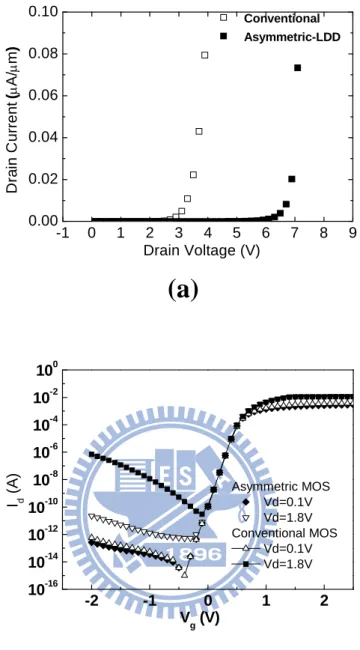
The DC drain breakdown voltage (BVdss) is determined at Vg of 0 V and Ids of 0.1
μA/μm. As shown in Fig. 3.2 (a), the BVdss is increased from 3.5 V for conventional
MOSFET to 6.9 V for asymmetric-LDD transistors DC drain breakdown voltage at gate voltage (Vg) of 0 V (BVdss) for conventional and asymmetric- LDD MOS
transistors[3.1.15]. Such almost 2 times improved BVdss is due to the designed wider
depletion region at drain side to allow higher applied voltage, which is vital for RF power application with large voltage swing. The larger BVdss is vital for RF power application
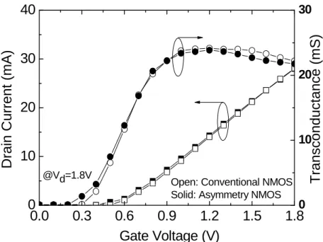
that has nearly 2 times larger swing voltage than DC drain bias voltage. The nearly the same drive current is at on-state which is 11.03 mA and 11.02 mA for conventional and asymmetric- LDD MOS transistors. Moreover, the asymmetric-LDD transistor shows a more than 4 orders of magnitude lower leakage current at -1.8 V (Fig. 3.2 (b)). This is also due to the wider depletion region at drain side to lower the reverse leakage current. T-Supreme and Medici device simulation is shown in Figs. 3.3 and 3.4, where the asymmetric-LDD devices decrease the peak electric field at drain side by the wider
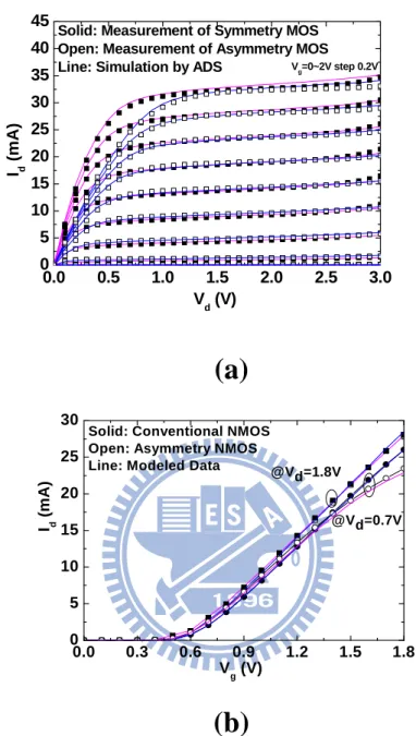
depletion region. Thus, our asymmetric MOS combines the merits of a MOSFET with the high breakdown voltage of a lateral bipolar transistor. The lower electric field can also improve the reliability by hot carrier injection (HCI). Fig. 3.5 shows the Id-Vg and gm-Vg
characteristics, where the asymmetric-LDD and conventional MOSFETs almost have the same peak gm of ~490 mS/mm. The nearly identical Id-Vg curves at high Vd led to close
trans-conductance (gm) that is important for small signal RF gain of |H21|2 and Gmax, ft
(gm/2πCg) and fmax discussed in following sections, where Cg is the gate capacitance.
In addition to the high breakdown voltage, the high drain current is also important for RF power application. The comparison of drive current of conventional and asymmetric- LDD 0.18 μm MOSFET were shown in the DC drain current-drain voltage
(Id-Vd) and drain current-gate voltage (Id-Vg) characteristics of Figs. 3.6(a) and (b),
respectively. The discrepancy between these two 0.18 μm devices is the slightly degraded
knee voltage and turn on resistance (Ron) at low Vd. However, the saturation drain current
(Id,sat) of these two devices is almost the same at high Vd. The close Id,sat is due to the
injected electrons from source can transient over the wide drain depletion region at fast saturation velocity.
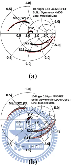
The RF S-parameters are shown in Figs. 3.7(a) and (b) for conventional and asymmetric-LDD 0.18 μm MOSFETs, respectively. The forward S21 is divided by 3 to fit
reverse S12 in asymmetric-LDD MOSFET that is due to the smaller gate-drain coupling
capacitance with wide depletion region at drain without n+ drain extension region.
To further analyze the small signal RF characteristics, we have plotted the frequency dependence on |H21|2 and Gmax as shown in Figs. 3.8, for conventional and
asymmetric-LDD 0.18 μm MOSFETs respectively. The |H21|2 follows the typical -20
dB/decade slope with increasing frequency and Gmax follows a -10 dB/decade slope at the
maximum stale gain (MSG) frequency region. The ft was obtained by extrapolating the
|H21|2 to 0 dB by the same slope of -20 dB/decade. The asymmetric device maintained a
high ft of 52 GHz and close to the 55 GHz value for conventional device. This is due to
nearly the same gm obtained in the Id-Vg characteristics shown in Fig. 3.5 at large Vd bias.
However, this method cannot be used for determining the fmax. This is because the Gmax
slope changes from -10 dB/decade to higher value at higher frequencies, where the Gmax
decreases from the MSG to maximum available gain (MAG). A device model is needed to analyze the MAG and fmax at higher frequency, beyond the maximum frequency
provided by network analyzer. Such device model, with simulation data in good agreement with measured DC, small signal S-parameters and large signal RF characteristics, are also indispensable for power amplifier circuit design.
3.3.2 Device modeling of the AMOSFET
Figure 3.9 shows the device model for asymmetric-LDD MOSFET. A Berkeley Short-channel IGFET Model (BSIM3) core is used to simulate the DC to RF characteristics, and additional sub-circuits were added for parasitic effects [3.3.1]-[3.3.3]. This asymmetric-LDD device model has smaller Cgd and larger drain series resistance
(RD) to simulate the slightly larger Ron and smaller S12, owing to the wide depletion
region without n+ doping at drain side. The typical value of RD is 11.33 Ω with smaller
gate-drain feedback capacitance (Cgd) of 1.86×10⁻¹⁰ F/m. The good accuracy of this
equivalent circuit model has been verified by the close agreements of simulated and modeled DC, S-parameters and RF gains (|H21|2 and MSG) shown in Figs. 3.6, 3.7 and
3.8, respectively.
Based on this well calibrated model shown in Fig. 3.9, we have further simulated the
Gmax to higher frequencies, where the Gmax degradation slope changes to ~25 to 40
dB/decade at MAG region. It is important to notice that a fmax of 115 GHz was obtained
by extrapolation asymmetric-LDD device model that is higher than the 97 GHz value in conventional device. This is due to the smaller reverse S12 shown in Fig. 3.7(b),
originated from the blocking n+ drain LDD extension underneath the drain spacer to give
high ft and fmax are in sharp contrast to the much-degraded values for LDMOS shown in
Table 3.1, at the same gate length.
Note that the transit frequency fT (=gm/2π(Cgd+Cgs)) and the maximum oscillation
frequency fmax are useful figures of merit to evaluate the dynamic performances of a
device dedicated to RF PA applications. The fmax of the MOS transistor can be estimated
by [3.3.4] gd g T max f / R C f = 8π ⋅ ⋅
The smaller Cgd increases fT and fmax. The gm of asymmetric-LDD device and
conventional device are almost the same under saturation region. Therefore, the asymmetric device obtains high fT and fmax which are almost same as conventional type.
The higher ft and fmax permit higher operating frequencies, which also give desired
larger |H21|2 and Gmax gain. Fig. 3.10 shows the VG dependences on ft, fmax and gm. The
peak ft occurs at almost the same VG as for the peak gm and a higher fmax is in the
3.3.3 RF power performance of the AMOSFET
We further measured the RF power characteristics. Figure 3.11 shows the output power and power-added efficiency (PAE) for conventional and asymmetric-LDD 0.18 μm devices measured at 2.4 GHz. The DC bias for these devices during measurements
are at peak gm for Vg. The Vd bias for conventional devices were at 1.8 V allowing a 2
times drain voltage swing close to BVdss that is higher at 2.5 and 3 V for asymmetric-LDD
MOSFET because of the higher BVdss. Good match between harmonic balance simulation
and measured data are also shown in Fig. 3.12. The RF output power at 2.4 GHz increased from 0.33 W/mm in conventional MOSFET to 0.43 and 0.54 W/mm in asymmetric-LDD device, which is equivalent to a 30% and 64% improvement. The peak PAE for asymmetric-LDD 0.18 μm device is 42% and 40% at Vd bias of 2.5 and 3 V
respectively, which is slightly lower than the 48% value for conventional device. However, the peak PAE for asymmetric-LDD device exists at higher RF power output than conventional ones with as much as 3 dB better output power.
Figure 3.12 further depicts the measured and simulated output power as functions of
Vd bias and frequency. The output power decreases with increasing frequency from 2.4 to
3.5 GHz that is due to the decreased gain at higher frequency. Figure 3.13 shows output power is higher at smaller gate lengths. This improvement is due to the higher power gain
(Gmax) at the shorter gate length. However, still significantly larger RF output power is
obtained in asymmetric-LDD 0.18 μm devices than conventional ones, which is simply
due to larger applied Vd bias permitting larger RF voltage swing. The higher RF power
density of asymmetric-LDD MOSFET is especially important for Si-based power amplifier design using power-combining techniques [3.3.5]. The higher power density in unit cell allows shorter transmission lines for RF power combination, where the RF loss to substrate for transmission line is one of the key issues for Si-based RF ICs [3.3.6]-[3.3.8].
Table 3.1 compares the performance with other devices [3.3.9]-[3.3.14]. Our device has better ft and fmax values than for LDMOS, better BVdss values than conventional
devices and the highest RF power density, while maintaining good drain efficiency and PAE.
The load-pull measurement offers no information of the actual voltage and current waveforms at time domain. We have performed the harmonic balance simulation on our well-calibrated large signal nonlinear model shown in Figs. 3.11 and 3.14. Figures 3.14 (a), 3.14 (b) and 3.14 (c) show the voltage and current swings as a function of time for 0.18 μm conventional and asymmetric-LDD MOSFETs biased at Vd of 1.8, 2.5 and 3 V,
respectively, with the same 10 dBm input power at 2.4 GHz.
with increasing VD bias from 3.8 V and 35.3 mA for VD=1.8 V, 4.9 V and 37.2 mA for
VD=2.5 V, and 6.2 V and 43.2 mA for VD=3 V. Therefore, the improved RF power
performance in asymmetric-LDD MOSFETs is due to the both larger voltage and current swings, which is in good agreement with the load-pull measurements shown in Fig. 3.11.
3.3.4 Linearity in saturation
One of the key factors for power amplifier is to have a good linearity. We have measured the ACPR of both conventional and asymmetric-LDD MOSFETs to examine the linearity characteristics. The ACPR measurement was standard W-CDMA with QPSK modulation from ROHDE & SCHWARZ SMIQ06B signal generator. The calibration was done by ATN on-wafer load pull system. As shown in Fig. 3.15, the ACPR degrades with increasing output power that is typical for RF power transistors. However, the asymmetric-LDD device shows improved ACPR with increasing Vd bias;
the improvement is as high as 8 dB better at peak PAE than conventional devices. This is due to the decreased reverse feedback coupling between gate and drain nodes from smaller Cgd that decreases the interference from adjacent channels. The much-improved
3.4
Conclusions
We have designed an asymmetric-LDD MOS transistor to increase the BVdss from
3.5 V to 6.9 V for larger output voltage and current swing and higher RF power delivery. Besides, good ACPR and PAE are obtained. This asymmetric-LDD MOSFET is fully embedded in the standard CMOS logic process provided by foundries without any process modification.
Fig. 3.1 The cross-sectional view of an asymmetry-LDD NMOSFET. The 0.18μm gate length, conventional MOSFETs have a wide spacer.
-1 0 1 2 3 4 5 6 7 8 9 0.00 0.02 0.04 0.06 0.08 0.10 Conventional Asymmetric-LDD Dr a in Cu rr e n t ( μ A/ μ m ) Drain Voltage (V)
(a)
-2 -1 0 1 2 10-16 10-14 10-12 10-10 10-8 10-6 10-4 10-2 100 I d (A ) V g (V) Asymmetric MOS Vd=0.1V Vd=1.8V Conventional MOS Vd=0.1V Vd=1.8V(b)
Fig. 3.2 (a) The Id-Vd characteristics at Vg of 0 V and (b) Id-Vg characteristics for
Fig. 3.3 The electric potential of conventional and asymmetric-LDD 0.18μm RF MOSFETs.
-0.2
-0.1
0.0
0.1
0.2
-4
-2
0
2
Lateral Emitter Base Collector
Ev
Band Energy (eV)
Distance
(μ
m
)Conventional NMOSFET at Vds=1.8V
Asymmetric NMOSFET at Vds=3.0V
EC
Source Depletion-Region Drain
Fig. 3.4 Energy band diagram of conventional and asymmetric-LDD devices. The thick undoped LDD lowers the electric field and increases VBD.
0.0 0.3 0.6 0.9 1.2 1.5 1.8 0 10 20 30 40 Gate Voltage (V) D rain C u rrent ( m A ) 0 10 20 30 Transconductance (m S)
Open: Conventional NMOS Solid: Asymmetry NMOS @Vd=1.8V
Fig. 3.5 Id-Vg and gm-Vg curves for conventional and asymmetric-LDD nMOSFETs with
0.0 0.5 1.0 1.5 2.0 2.5 3.0 0 5 10 15 20 25 30 35 40 45 I d (mA) Vd (V) Vg=0~2V step 0.2V
Solid: Measurement of Symmetry MOS Open: Measurement of Asymmetry MOS Line: Simulation by ADS
(a)
0.0 0.3 0.6 0.9 1.2 1.5 1.8 0 5 10 15 20 25 30 @Vd=0.7V @Vd=1.8VSolid: Conventional NMOS Open: Asymmetry NMOS Line: Modeled Data
V
g (V)
I d
(mA)
(b)
Fig. 3.6 Measured and simulated (a) Id-Vd and (b) Id-Vg characteristics for 10-gate-finger
0.5 1.0 2.0 5.0 -0.5j 0.5j -1.0j 1.0j -2.0j 2.0j -5.0j 5.0j 10-finger 0.18 μm MOSFET Solid: Symmetry NMOS Line: Modeled Data
S12 Mag(S21)/3 S22 S11
(a)
0.5 1.0 2.0 5.0 -0.5j 0.5j -1.0j 1.0j -2.0j 2.0j -5.0j 5.0j 10-finger 0.18 μm MOSFET Solid: Asymmetric-LDD MOSFET Line: Modeled dataS22 S11
S12 Mag(S21)/3
(b)
Fig. 3.7 Measured (solid symbols) and simulated (line) S-parameters for (a) conventional and (b) asymmetric-LDD 0.18 μm RF MOSFETs.
1 10 100 0 5 10 15 20 25 30 35 40 0 5 10 15 20 25 30 35 40 |H 21 | 2 (dB ) Frequency (GHz)
Symbol: Measured Data Line: Modeled Data
G ma x (dB ) Symmetric Asymmetric fT = 55GHz 52GHz fmax= 97GHz 115GHz
Fig. 3.8 Measured and simulated |H21|2,Gmax, ft and fmax characteristics for conventional
and asymmetric-LDD 0.18 μm RF MOSFETs. The ft was obtained by extrapolating |H21|2
to 0 dB with a -10 dB/decade slope. The fmax was obtained by extrapolating the MAG to 0
RS Cds RD RG RSB Rds RDBR B DSG DSS DDG DDD D S G B BSIM RS Cds RD RG RSB Rds RDBR B DSG DSS DDG DDD D S G B BSIM
Fig. 3.9 The self-consistent device model of asymmetric-LDD 0.18 μm RF MOSFETs to simulate the DC, small signal S-parameters to large signal RF power characteristics.
0.0 0.3 0.6 0.9 1.2 1.5 1.8 0 20 40 60 80 100 120 140 0 10 20 30 40 50 60 70 80 90 ft gm
Open: Conventional NMOS Solid: Asymmetry NMOS Line: Modeled Data
Conventional NMOS Asymmetry NMOS f t & f ma x (GHz) Vg (V) fmax @Vd=1.8V g m (m S)
Fig. 3.10 Measured and simulated ft, fmax and gm characteristics of conventional and asymmetric-LDD 0.18μm RF MOSFETs.
-30 -25 -20 -15 -10 -5 0 5 10 15 -12 -8 -4 0 4 8 12 16 20 Ou tp u t P o wer (d B m) Ga in (d B ) Input Power (dBm) P o wer -A dded E fficiency (% ) 0 10 20 30 40 50 60 70 80 90 100 Conventional NMOS Asymmetric NMOS Vd=2.5V Asymmetric NMOS Vd=3V
Line: Modeled Data
10-finger 0.18 μm MOSFET
Fig. 3.11 Measured and modeled RF output power and PAE at 2.4 GHz for both types of device.
2.0 2.5 3.0 3.5 4.0 0.0 0.1 0.2 0.3 0.4 0.5 0.6 0.7 0.8 Asymmetric Device Vds=3V Asymmetric Device Vds=2.5V Conventional Device Pow e r D e nsity (W/mm) Frequency (GHz) Dash Line:Model Solid Line:Measurement
0.10 0.15 0.20 0.25 0.30 0.35 0.40
0.0
0.2
0.4
0.6
0.8
Asymmetric Device Vds=3V Asymmetric Device Vds=2.5V Conventional DevicePower Densit
y (W
/m
m)
Gate Length (
μm)
0 100 200 300 400 500 600 700 800 900 -4 -2 0 2 4 6 8 10 -10 0 10 20 30 40 50 V o lt ag e ( V ) Time (psec) Pin=10dBm, Vd=1.8V, Vg=1.2V Curre nt ( m A) Drain Voltage Drain Current (a) 0 100 200 300 400 500 600 700 800 900 -4 -2 0 2 4 6 8 10 -10 0 10 20 30 40 50 V o lt ag e ( V ) Time (psec) Pin=10dBm, Vd=2.5V, Vg=1.2V Curre nt (mA) Drain Voltage Drain Current (b) 0 100 200 300 400 500 600 700 800 900 -4 -2 0 2 4 6 8 10 -10 0 10 20 30 40 50 V o lt age (V ) Time (psec) Pin=10dBm, Vd=3V, Vg=1.2V Curren t (mA) Drain Voltage Drain Current (c)
Fig. 3.14 Input and output voltage and current swing of the devices at the 10 dBm RF input power for (a) Conventional (ZS=195+j168.8, ZL=95.1+j20.9), (b)
asymmetrical-LDD at Vd=2.5V (ZS=195+j168.8, ZL=121.2+j29.8) and (c) at Vd=3.0V
0
5
10
15
-50
-40
-30
-20
ACPR (dBc)
Output power (dBm)
Conventional device Asymmetric device Vds=2.5V Asymmetric device V ds=3VFig. 3.15 ACPR vs. output power of conventional and asymmetric-LDD 0.18μm RF MOSFETs @ 2.4 GHz.
Table 3.1 Comparison of LDMOS and Asymmetry MOSFET published data with that from this work (*Calculate from P1dB;**4dB compression;**6dB compression)
ft (GHz) fmax (GHz) BVdss (V) Power (W/mm) @ Freq. PAE (%) @ Freq. &VD Drain Eff. (%) @ Freq. &VD Device [3.3.9] 31 47 15.5 0.21 1.8GHz 48 1.8GHz, 3.6V 75 1.8GHz, 3.6V 0.3 μm LDMOS [3.3.10] 18 - 15 - 60 0.9GHz, 12V - 0.18 μm LDMOS [3.3.11] 15 38 45 0.25* 1.9GHz 41 2.4GHz, 12V 46 2.4GHz, 12V 0.15 μm LDMOS [3.3.12] 32 26 14 0.092 0.9GHz 53 0.9GHz, 3.5V 71 0.9GHz, 3.5V 0.3 μm LDMOS [3.3.13] 25 11 5.4 0.1** 2.4GHz 39 2.4GHz, 2.5V 45 2.4GHz, 2.5V 0.24 μm CMOS [3.3.14] 140 100 3.2 0.353*** 2.4GHz 43 3GHz, 1.5V 46 3GHz, 1.5V 90 nm CMOS This Work 55 97 3.5 0.33 2.4GHz 48 2.4GHz, 1.8V 60 2.4GHz, 1.8V 0.18 μm Conventional MOS 52 115 6.9 0.54 2.4GHz 41 2.4GHz, 3V 52 2.4GHz, 3V 0.18 μm Asym. MOS
Chapter 4
A Single Chip Implementation for 2.4GHz
Linear Power Amplifier
4.1 Introduction
The design of a RF CMOS power amplifier (PA) is challenging [4.1.1]-[4.1.4], due to the limited output voltage swing of MOSFETs and the RF loss in passive devices. Although the RF power gain has improved with evolving technology, an accompanying decrease in the MOSFET breakdown voltage [4.1.3]-[4.1.4] poses difficulties in PA design. High-power PAs also consume large chip area due to the poor power density of MOSFET. To increase the RF output power and power-added- efficiency (PAE), a switching type PA has been proposed [4.1.1], but necessitates to trade-off the linearity and the gain that are essential for applications such as in WCDMA. Some RF CMOS PAs perform well, but show non-optimized linearity performance or lacking of linearity data [4.1.2], [4.1.4]. A linear PA, using high-breakdown voltage 0.35μm MOSFETs for the power stage and higher gain 0.18μm MOSFETs for the driver stage, has shown good
performance and EVM [4.1.3]. However, this architecture is limited to low-frequency operation by the slow speeds of 0.35μm transistors in the power stage.
To address this challenge, we have developed an asymmetric-LDD MOSFET [4.1.5] that meets the required large RF output power and high-frequency performance.
This new RF power device was fabricated in conventional foundry logic processes, by using an n+ drain-extension blocking mask but no extra processing step. The
asymmetric-LDD MOSFE shows the transistor breakdown voltage and device structure, where the breakdown voltage can be improved by a factor of ~2 from 3.5 to 6.9 V [4.1.5]. In this thesis we describe a single-ended two-stage PA, implemented using the asymmetric-LDD MOSFETs. The output power improves with increasing bias voltage from 1.8, 2.5 to 2.75 V, and matches simulations well. Such improved power performance, along with high RF output power, high power density, excellent linearity and high efficiency are especially important for MOS PAs for communications.
4.2 Architecture
The single-ended 2-stage PA shown in Fig. 4.1 adopts a class A operation for driver stage and class AB for power stage, which has been optimized for gain, efficiency and linearity. In both stages, asymmetric-LDD MOSFETs were implemented in the foundry-standard 0.18μm 1P6M process, with n+ drain-extension blocking mask. The
number of unit cells for the driver and power stages were determined considering the power-level, gain, matching and linearity. Here we used 10 and 40 unit cells for the driver and power stages with a size ratio of 1:4. The impedances of the input, inter-stage and output matching were selected to get a compromise between power and efficiency, with the aid of load- and source-pull simulations. For practical application, we designed the PA to have on-chip matching. The use of on-chip inductors is more of a challenge compared with using off-chip inductors [4.1.2]. The reduced RF power performance for a PA with on-chip inductors, compared with the off-chip case, is due to the well-known poor Q-factor arising from substrate losses.
4.3 Small-signal characteristics
To verify the chip design, we first measured the small signal S-parameters shown in Fig. 4.2. A 19.6 dB gain and 17 dB input and output return loss were measured- this is consistence with EM post-simulation data.
4.4 Large signal characteristics
The measured and simulated RF power characteristics appear in Fig. 4.3. At 2.4 GHz there was good agreement between the measured output power, gain and PAE with the simulated results. The output power, at 1dB compression (P1dB), increases with
increasing bias voltage – which was also simulated. The PA achieved large output power of 23.2 dBm, high P1dB of 21.5 dBm and good PAE of 29.6% at 2.4 GHz and 2.75 V bias
with standard on-chip inductors. A simulation indicated this would improve by as much as ~4 dB if using off-chip inductors in this PA, which is due to the improved Q-factor of off-chip inductors. This data are better than or comparable well with other PAs published in literature [4.1.1]-[4.1.7].
4.5 Linearity
Fig. 4.4 shows the Adjacent Channel Power Ratio (ACPR) measurement under standard W-CDMA with QPSK modulation. The calibration was done by ATN on-wafer load pull system. The ACPR improves with bias. At a 2.75 V, the PA had an ACPR of -49 dBc at a 10 dBm output power, and -36 dBc at 18 dBm, at 2.4 GHz. The good ACPR performance is due to the decrease in the adjacent channel reverse feedback. This is originated from the smaller gate-drain coupling capacitance (Cgd) by removing the n+
extension region at the drain side of the devices. These results are even competitive with PAs designed specifically to obtain good linearity [4.1.6].
Fig. 4.5 shows the chip image. A small 1-mm×1.1-mm die size is reached, which is significantly smaller than using transformer output matching [4.1.3]. This is due to the higher output power density using this new power cells.
4.6 Conclusion
Using standard 0.18μm 1P6M CMOS process with n+ LDD blocking mask, the
on-chip matched MOS PA has high 23.2 dBm output power, 19.6 dB power gain, 29.6% PAE, -36 dBc ACPR at 18 dBm output power and small die size of 1-mm×1.1-mm. These results are better than or comparable with the best data reported in literature.
1 2 3 4 5 6 7 8 -40 -30 -20 -10 0 10 20 S21 S11 S22 Symbols:Measured Data Lines: Modeled Data
S-Parameter (dB)
Frequency (GHz)
-10 -5 0 5 10 8 12 16 20 24 28 Lines: Simulation At 2.75V At 2.5V At 1.8V O u tpu t Po wer (d Bm ) Input Power (dBm) Po we r-Add ed Effi ci en cy (%) Gain ( d B ) Symbols: Measured Data 0 20 40 60
-10 0 10 20 -60 -40 -20 ACPR ( d B c ) Output Power (dBm) VD = 1.8V VD = 2.5V VD = 2.75V
Chapter 5
RF AMOSFETs on SiC Substrate
5.1 Introduction
The Si RF MOSFETs are now widely-used for wireless communications, due to the improvements of the larger RF gain, higher current-gain (|H21|2) cut-off frequency (ft) and
better power-gain (Gmax) maximum oscillation frequency (fmax) with transistor
down-scaling and technology evolution[5.1.1]-[5.1.3]. We previously developed an asymmetric-LDD MOSFET [5.1.4] that met the requirement large RF output power and high-frequency performance. This new RF power device (AMOSFET) can be fabricated in standard foundry logic processes by blocking the n-drain extension using LDD mask without extra processing step.
Advanced complementary metal oxide semiconductor (CMOS) technology is one of the candidates for System-on-Chip (SOC) due to integration and low cost. However, the decay factor of MOSFET performance is the self heating effect [5.1.5] and substrate loss [5.1.6]. Self heating effect represents the heating of the device due to its internal power dissipation, especially in high current devices. It results in a reduction of the drain current and the negative output conductance effect. Additionally, the lossy Si-substrate causes the
parasitic effect of the coupling capacitance and loss the RF signal to substrate. In this paper, we reported the DC and RF performance can be improved ~6% of AMOSFET with ultra thin Si substrate (50 μm) and bonding onto SiC substrate. The thermal conductivity
is 4.9 W/cm-K of SiC substrate compared to 1.5 W/cm-K of silicon substrate. The resistivity of VLSI-standard Si substrates is 10 Ω-cm lower than that of the
semi-insulating SiC substrates is ~105 Ω-cm. The substrate removing is using CMP process after CMOS IC processes. Also, the active devices after thinned-down and transfer on plastic had been reported [5.1.7]-[5.1.9]. However, the self heating effect of high current active device is serious due to the worse thermal conductivity. Therefore, the SiC substrate base device is becoming a good candidate for improving DC and RF power performance.
5.2 Experiment Procedure
A foundry standard 0.18 μm 1-poly-6-metals (1P6M) logic process was used in this
study. To increase the breakdown voltage, the drain LDD region was removed by an n ion-implantation blocking mask to form the AMOSFET [5.1.5]. The p-type region underneath the drain spacer forms a wider depletion region to allow larger applied drain voltage. Multiple gate fingers layout has been used, which have 40-gate-finger AMOSFET with 0.18 μm gate length and 5 μm width for milli-watt RF power
application. To achieve integration onto SiC substrate, we first thinned down the Si substrate from 550 μm to 50 μm by using a Chemical Mechanical Polish (CMP) procedure. The thinned die was then transfer onto a 275 μm thick SiC substrate. Fig.
5.1(a) shows an image of the fabricated die on SiC substrate (holding by hand- the background). The 50 μm Si substrate thinned-down thickness of the optical measurement
is shown in Fig. 5.1(b). The semi-insulating SiC substrate had a resistivity of 105 Ω-cm. The devices were fabricated on 8-in wafers at an IC foundry. The small signal S-parameters were measured up to 22 GHz by CASCADE probe station and LRRM standard calibration procedure using HP8510C network analyzer. The intrinsic device characteristics were obtained by open and short two step de-embedding procedures [5.2.1]-[5.2.2]. The RF power characterization was carried out by on-wafer measurements at 2.4 GHz using an ATN load-pull system, where the input and output
5.3 DC Characteristic of 0.18
μm RF AMOSFETs on SiC Substrate
The drive current of AMOSFETs with 200 μm with and 0.18 μm length before andafter thinned-down process are shown Fig. 5.2. After thinned-down and transfer procedure, the drain current increases at high Vg ( >0.6 V).However, the drain current
of these two devices is almost the same at small Vg ( < 0.6 V). This is because of the
SiC has good heat dissipation to reduce the self-heating effect. The self-heating effect could be verified from the pulse IV measurement [5.3.1] due to the “cold” device characteristics. Figure 5.3 shows the increasing percentage of the drain current at Vd = 1.8
V bias condition. The reduction of self-heating effect is significant at higher drain current
Id.
Figure 5.4 shows the transconductance enhancement of AMOSFET before and after thinned-down procedure. The thinned-downed on SiC substrate AMOSFET shows the higher gm characteristic than on VLSI-standard substrate. The gm value increase from
88.95 mS to 93.4 mS which is 5 % enhancement. The enhancement trend of DC performance is due to good heat dissipation of 50 μm Si on SiC substrate.
5.4 Small-signal characteristics
The RF S-parameters from 1.1 GHz to 22 GHz of AMOSFET before and after thinned-down procedure were measured. Fig. 5.5 shows the current gain (⎪H21⎪2) and
Gmax as a function of frequency, for both AMOSFET. A cutoff frequency ft of 61 GHz was
obtained from the measured S-parameters for the thinned AMOSFET device. This value is higher than the 57 GHz value found for the VLSI-standard Si Substrate AMOSFET. This higher ft in the thinned-down AMOSFET device is consistent with the gm in Figure
5.4. The ft is given by g m T C g = ω
where Cg is input capacitance and ωT = 2 *π* fT. Therefore, the thinned-down
AMOSFET has the higher ft due to the higher gm. The reduced self heating effect
improves the RF small signal characteristic.
The Gmax which follows a -10 dB/decade slope at the maximum stable gain (MSG)
frequency region was obtained from the measured S-parameters on VLSI-standard Si substrate and 50 μm Si substrate on SiC AMOSFET device. The thinned-down
AMOSFET maintained a higher Gmax than the VLSI-standard Si substrate AMOSFET
device in Fig. 5.5. Therefore the higher fmax is obtained by extrapolation for the