國 立 交 通 大 學
光 電 工 程 研 究 所
碩士論文
非極性"a"面氮化銦鎵多重量子井成長在奈
米圖樣基板之光學特性研究
Optical properties of a-plane
In
0.2
Ga
0.8
N/GaN multiple quantum wells
grown on nanorod GaN templates
研
研
究
究
生
生
:
:
詹
詹
惟
惟
雯
雯
..指
指
導
導
教
教
授
授
:
:
盧
盧
廷
廷
昌
昌
教
教
授
授
郭
郭
浩
浩
中
中
教
教
授
授
中
中
華
華
民
民
國
國
九
九
十
十
九
九
年
年
七
七
月
月
非極性"a"面氮化銦鎵多重量子井成長在奈米圖樣基板之光學特性研究
Optical properties of a-plane In
0.2Ga
0.8N/GaN multiple quantum
wells grown on nanorod templates
研究生:詹惟雯 Student: Wei. Wen. Chan
指導教授:盧廷昌 教授 Advisor:Prof. Tien-Chang Lu
郭浩中 教授 Prof. Hao-Chung Kuo
國 立 交 通 大 學
光電工程研究所
碩 士 論 文
A Thesis
Submitted to Institute of Electro-Optical Engineering College of Electrical Engineering and Computer Science
National Chiao Tung University in Partial Fulfillment of the Requirements
for the Degree of Master
In
Electro-Optical Engineering
June 2010
非極性"a"面氮化銦鎵多重量子井成長在奈米圖樣基板之光學特性研究
研究生:詹惟雯 指導教授:盧廷昌 教授 郭浩中 教授交通大學光電工程研究所
摘要
在本論文中,我們利用有機金屬化學氣相沉積法成長非極性”a”平面氮化 銦鎵/氮化鎵多重量子井的結構,樣品的差異為氮化鎵基板中不同的奈米柱 (Nanorod)深度。在特性分析中,包含了光學與結構特性上的相關研究;在發光 特性方面,所利用的是光激發螢光光譜(PL)進行樣品的光學特性分析,結構及相 關成分的研究包含了掃描式和穿透式電子顯微鏡圖像、原子力顯微鏡、X射線繞 射…。 由AFM、TEM可知,奈米柱深度越深再成長的氮化鎵基板,表面的質地越好, 藉由變溫PL的量測,可以得到室低溫強度比隨著奈米柱深度越深值越大,活化能 也提升,意味著減少樣板的缺陷,多重量子井的侷限能力會提升;在變功率的PL 實驗中,樣品的發光波長不隨者雷射功率增加而改變,得知非極性面成長的氮化 銦鎵多重量子井能確實抑制QCSE的效應。在非極性結構的極化發光特性量測中, 我們發現發光極化率、能量差會隨著奈米柱深度越深而降低,顯示了應力的改 變,再經由模擬得到驗證。 接著,我們量測變溫變功率 PL 的內部量子效率,得到經由奈米柱深度 1.7 微米(最深)成長的樣品是 39%,而直接成長的樣品是 13%,再透過實驗數據 的分析,得到非輻射係數(A),隨著奈米柱深度越深而降低,與 TEM 估算出來的 錯位密度缺限變化相吻合,所以在奈米柱深度 1.7 微米有最佳的載子捕捉及放光 效率。Optical properties of a-plane In0.2Ga0.8N/GaN multiple quantum wells grown on
nanorod GaN templates
Student: Wei Wen Chan Advisors: Prof. Tien-Chang Lu Prof. Hao-Chung Kuo
Institute of Electro-Optical Engineering, National Chiao Tung University
Abstract
In this thesis, we investigated a-plane InGaN/GaN multiple quantum wells were
grown on r-plane sapphire by metal organic chemical vapor deposition, and the
difference of samples is nanorod depth of a-plane GaN templates. We utilized several
methods including photoluminescence(PL), atomic force microscopy(AFM), and
transmission electron microscopy(TEM)to investigate the optical characteristics and
material structures of our samples.
We have known that the crystal quality of a-plane GaN films was improved by
using epitaxial lateral overgrowth on a nanorod GaN template by AFM and TEM.
And from the temperature dependent PL measurement, we get the result which the
value of IQEPL and activation energy is higher when the etching depth of nanorods is
deeper. It means carries confinement in MQWs was enhanced by lowering defects of
a-plane GaN templates. Moreover, the un-shift emission peak from the
power-dependent PL measurement indicated the absence of QCSE within our samples.
injection carrier density and scattering.
In the second part, we measure the internal quantum efficiency(IQE)of the
MQWs, and the IQE of a-plane InGaN/GaN MQWs are approximately 39%(1.7um)
more than 13%(as-grown). Next, using the measured data and knowing the B value,
one can obtain nonradiative coefficient A. The measured nonradiative recombination
coefficient A decreased one order as the etching depth increases from 0 to 1.7 um. It
matched the variation of threading dislocation density and we could observe the best
致謝
時光飛逝,沒想到馬上就輪到我畢業了,回頭想想這兩年實驗室的點點滴 滴,其實也蠻令人感傷的,首先一定要先感謝我們的三位老師:王老師、盧老師 和郭老師,相信未來三位老師們一定能帶領實驗室為台灣做出更好的研究成果。 可以順利的完成研究內容,最感謝的就是碩均學長,提供我一系列的樣品, 以及指導我如分析數據,一起討論下一步該怎麼做,不會無謂的浪費時間,有效 地解決問題;另外也非常感謝輝閔學長、俊榮學長、清華學長和卓木學長,在研 究上都對我有非常大的幫助。在碩士的兩年生活裡,與我生活關係最密切的就是 一起同甘共苦的同學們,謝謝依嚀、婉君,從大學一起到研究所,我們總是有聊 不完的話題,感覺妳們常常要聽我發牢騷,是我研究所最好的伴;也謝謝永吉、 大為等碩二的同學,大家常常一起吃飯、聊天、玩樂、修課,讓我的碩士生活更 多采多姿。 最後謝謝我的家人,感謝我的爸爸媽媽的支持,讓我順利完成學業,謝謝你 們。Content
Abstract (in Chinese)……….………..………..i
Abstract (in English )………..……….ii
Acknowledgement………...………....iv
Content………...……….…...v
List of Figures...vii
Chapter 1 Introduction and Motivation
1.1 The development of Ⅲ-Nitride nanostructure from c-plane to a-plane…….11.2 The characteristics of a-plane GaN films……….2
1.3 Fabrication of nanostructure materials………...3
1.4 Motivation………4
Chapter 2 Properties of nonpolar multiple quantum wells (MQWs)
structure
2.1 Quantum confinement effect in semiconductor nanostructure………...92.2 The basic concept of nonpolar nanostructure……….11
2.3 In-plane light polarization effect in nonpolar nanostructure………12
Chapter 3 Sample growth and experimental instrument
3.1 Growth mechanism of InGaN/GaN MQWs using metal organic chemical vapor deposition (MOCVD)………....173.2 Transmission Electron Microscope (TEM), Atomic Force Microscopy(AFM)and Scanning electron microscope (SEM) 3.2.1 Transmission Electron Microscope (TEM)……….19
3.2.3 Scanning electron microscope (SEM)……….24
3.3 Photoluminescence……….25
Chapter 4 Optical properties of a-plane In
0.2Ga
0.8N/GaN multiple
quantum wells with nanorod templates
4.1 Introduction………294.2 Samples preparation and growth………30
4.3 Temperature dependent photoluminescence a-plane InGaN/GaN MQWs……….32
4.4 In-plane polarization effect of a-plane InGaN/GaN MQWs emission…………...35
4.5 Nonpolar characteristics of a-plane InGaN/GaN MQWs………38
4.6 Measuring internal quantum efficiency and fitting nonradiative recombination coefficient of GaInN/GaN MQWs with different dislocation densities…………39
4.7 Conclusion………..43
Chapter 5 Characteristics of emission polarization in a-plane
nanorods embedded with InGaN/GaN MQWs
5.1 Introduction………645.2 Experiment………65
5.3 Results and discussions………..67
5.4 Conclusion..………71
Chapter 6 Conclusion and future work
6.1 Conclusion………..796.2 Future work………....80
List of Tables
Table 4.3.1 The experimental results represent the IQE of the InGaN/GaN MQWs samples of a-plane InGaN/GaN MQWs……….49 Table 4.3.2 The fitting results of activation energy of a-plane InGaN/GaN MQWs with different nanorod depth………50 Table 4.4.1 The degree of polarization and peak energy shift with different nanorod depth at 300K………..54 Table 4.6.1 The value of nonradiative coefficient A with different nanorod depth at 300K………60 Table 5.3.1 The fitted activation energy (Ea) for PL quenching for all as-grown and
List of Figures
Fig. 1.1.1 Band bending resulted from QCSE in polar quantum well with different
thicknesses……….7
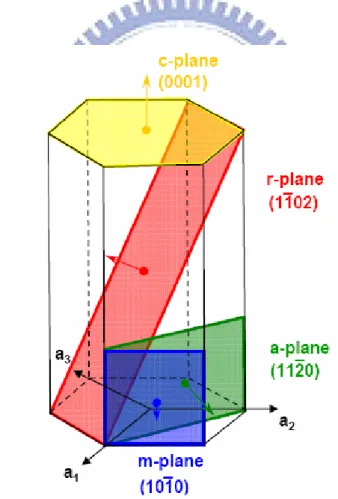
Fig. 1.1.2 The planar relation and orientation in hexagonal crystal structure…………7
Fig. 1.3.1 Dimension of nanostructure and corresponding density of stat……….8
Fig. 1.3.2 The carrier behavior in three dimensional confinement structure…………8
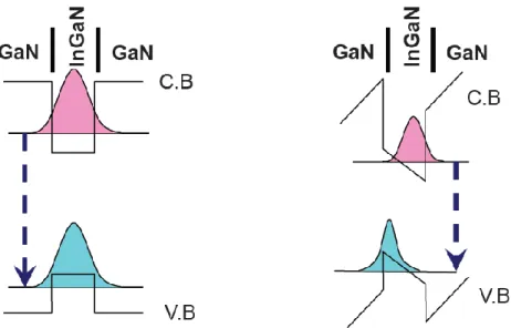
Fig. 2.3.1 The band diagrams of (a) nonpolar quantum wells and (b) polar quantum wells……….16
Fig. 2.4.1 The definition of the coordinate system for our samples……….17
Fig. 3.1.1 MOCVD system………...………27
Fig. 3.2.2 Block diagram of atomic force microscope………...27
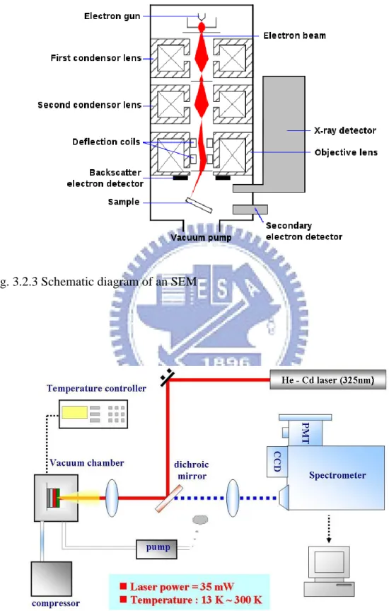
Fig. 3.2.3 Schematic diagram of an SEM………28
Fig. 3.3.1 The schematic diagram of photoluminescence setup………28
Fig. 4.2.1 (Color online) Flow chart of a-plane GaN NRELOG process.………..…..45
Fig. 4.2.2 (Color online) SEM images of (a) Fabricated GaN nanorods. (b) Mask density of GaN template. (c) Initial MOCVD regrowth on a-plane GaN nanorods in 90° angle of view, and (d) fully coalesced a-plane GaN films in cross-sectional view………...45
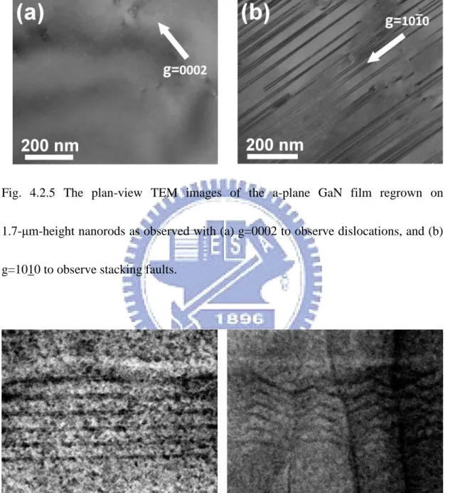
Fig. 4.2.3 9 um2 AFM images of the as-grown sample and the NRELOG sample, respectively……….46
Fig. 4.2.4 The schematic drawing of sample structure………46
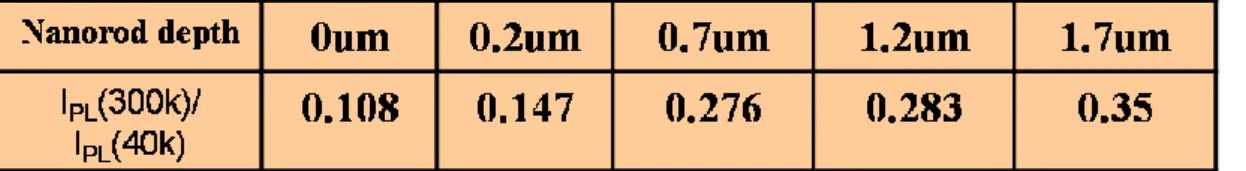
Fig. 4.2.5 The plan-view TEM images of the a-plane GaN film regrown on 1.7μm height nanorods as observed with (a) g=0002 to observe dislocations, and (b) g=1010 to observe stacking faults………..47 Fig. 4.2.6 Typical bright-field cross-sectional TEM image of the a-plane InGaN/GaN
region in higher threading dislocation density……….47 Fig. 4.3.1 (Color online) The PL emission spectra under temperature varied from 40 to 300 K. They imply the samples with nanorod templates varied from 0um to 1.7um………...48 Fig. 4.3.2 (Color online) The normalized PL intensity plotted as a function of 1/T for the samples with different nanorod depth. The symbols stand for the measurement results and the solid line means the fitted curve of the five samples. The number labeled near the curves represents the fitted activation energies………....49 Fig. 4.3.3 The temperature-dependent PL results of the five samples shows the dominate wavelength shift from 40 to 300 K………...50 Fig. 4.4.1 The schematic of experimental PL setup for the in-plane polarization…...51 Fig. 4.4.2 (a) Room temperature polarization-dependent PL spectra for polarization angles from 0oto 90o with nanorod templates varied from 0um to 1.7um.52 Fig. 4.4.2 (b) The symmetric of normalized PL intensity versusbthe polarization
degree from 0o to 360o………53
Fig. 4.4.3 The polarization ratio plotted as the function of nanorod etching depth at 300K……….54 Fig 4.4.4 Simulated polarization degree with different injection carrier density of In0.25Ga0.75N/GaN MQWs at 300K……….55
Fig 4.4.5 PL spectra simulated as a function of x’-polarized and y’-polarized of In0.25Ga0.75N/GaN MQWs at 300K varied strain from 1a to 2.5a…………56
Fig 4.4.6 Simulated polarization degree with different strain of In0.25Ga0.75N/GaN
MQWs at 300K……….56 Fig. 4.5.1 PL spectra with different nanorod depth plotted as a function of excitation power at 300K………..57
Fig. 4.5.2 Power-dependent PL fitting result for InGaN/GaN MQWs at 300K…….58 Fig. 4.6.1 Relative PL quantum efficiency as a function of excitation power density for all samples measured at 300 and 20 K………59 Fig. 4.6.2 PL spectra with different nanorod depth plotted as a function of excitation power at 20K………60 Fig. 4.6.3 (Color online) Generation rate G as a function of integrated PL intensity IPL
of 1.7um and fitted curves obtained using Eq. (4.6.4)……….61 Fig. 4.6.4 (Color online) Nonradiative coefficient A as a function of nanorod etching
depth……….62 Fig. 4.6.5 (Color online) The internal quantum efficiency of fitting value compared
with experimental value as a function of nanorod etching depth…………63 Fig. 5.2.1 (Color online) (a) The schematic of the a-plane InGaN/GaN MQWs nanorod fabrication process. (b) The birds-view (left) and cross-sectional (right) FESEM image of the fabricated a-plane InGaN/GaN MQW nanorods. The density, diameter and heights of the nanorods were and 1×109 cm−2, 250 nm and 0.6 µm, respectively……….73 Fig. 5.3.1. (Color online) The integrated PL intensity of nanorod samples with indium composition of (a) 0.09, (b) 0.14, (c) 0.24, and (d) 0.30 at different polarization angles at room temperature………..74 Fig. 5.3.2 (Color online) The polarization ratio plotted as the function of indium compositions for the as-grown and nanorod samples………..75 Fig. 5.3.3 (Color online) The temperature-dependent PL spectra for the (a) as-grown and (b) nanorod samples with indium composition of 0.09. The temperature increases from 20 K to 300 K with 20 K interval………76 Fig. 5.3.5 (Color online) The integrated intensity ratio of the PL to PH peaks plotted as
Chapter 1 Introduction and Motivation
1.1 The development of Ⅲ-Nitride nanostructure from c-plane to a-plane
In the past, GaN-based semiconductor had attracted much attention for
commercial applications in developing high quality optoelectronic devices. A number
of studies have reported laser diodes and light emitting diodes grown on sapphire、
6H-SiC、or free-standing GaN along c-plane [0001] crystal orientation. However, the
optoelectronic device grow along [0001] axis that the built-in electric field may exist in
the nanostructure. The built-in electric field consists of spontaneous polarization and
piezoelectric polarization. The built-in electric field would result in potential bending
which called quantum confined stark effect (QCSE) [1, 2]. This would result in
decreasing the oscillation strength of the separation of electron-hole pairs. Also, the
carrier recombination rate and the internal quantum efficiency (Fig. 1.1.1) would be
reduced. In order to improve the internal quantum efficiency, the issue related to
overcome the built-in electric field within the multiple quantum wells (MQWs) is very
important.
Recently, several groups have grown samples on the nonpolar structures to
eliminate the built-in electric field. There are two approaches of nonpolar structures in
common. One is growing [1010] m-plane heterostructures on γ -LiAlO2(100) by
other one is growing [1120] a-plane heterostructures on r-plane sapphire or a-plane SiC
by metalorganic vapor-phase (MOVPE) [5-7]. The planes with different orientations of
hexagonal wurtize structure of GaN are showed in Fig. 1.1.2. Nowadays, nonpolar
structure has been used to grow AlGaN/GaN and InGaN/GaN heterostructures.
The optical characteristics of c-plane heterostructures have been investigated
intensively [8-9]. However, the optical properties of nonpolar heterostructures have
been still worth studying. In these few years, many groups have made efforts on the
structure growth condition and the light efficiency improvement such as nonpolar and
nanorod structures [5, 10-12]. In this thesis, we will discuss the optical properties and
the carrier recombination mechanisms of nonpolar a-plane InGaN/GaN MQWs.
1.2 The characteristics of a-plane GaN films
Recent studies of InGaN/GaN multiple quantum wells demonstrate that it is
possible to eliminate such polarization fields along the nonpolar orientation. However,
the difficulty to utilize nonpolar GaN is not a suitable substrate for heteroepitaxial
a-plane GaN growth. In general, the threading dislocation (TD) density of ~ 3×10¹⁰
cm−2 and a basal stacking fault density of ~ 3.5×105 cm−1 were commonly observed in
a-plane GaN grown on r-plane sapphire. The TDs in GaN act as nonradiative recombination centers which are responsible for poor internal quantum efficiency
device performance. Lateral epitaxial overgrowth (LEO) techniques have been
employed to achieve defect reduction in nonpolar GaN. Previous LEO methods
include SiNx nanomask LEO [13],single-step LEO [14], selective area LEO (SALE)
[15],sidewall LEO, [16]and so on.
However, the regrowth thickness of these LEO techniques is usually larger than
20 um to achieve a better coalescence surface, causing the difficulty in layer
uniformity control. In this thesis, we propose an approach of lateral overgrowth on
nanorod a-plane GaN template to realize the defect reduction and quality
improvement in the subsequently grown a-plane GaN layer. Compared with the
above-mentioned LEO techniques, the nanorod epitaxial lateral overgrowth
(NRELOG) is highly advantageous for thinner.
1.3 Fabrication of nanostructure materials
Low dimension structure as the active layer was widely applied in these optical devices to operate in low threshold current, reduce temperature sensitivity and
enhance the emitting efficiency due to quantum confine effect [4-5]. Because of the
different dimensional confinement of carrier and density of state, the nanostructure
can be classify into quantum well (QW), nanowire and quantum dot (QD) by their
density of state as shown in Fig. 1.3.1. The bulk material has three dimensional
continues above energy band-gap. Then two dimensional structures, such as quantum
well, is a step function due to one dimensional confinement of carrier. With
decreasing the degree of freedom of carriers, the density of state of zero-dimensional
structure, as quantum dot, manifest delta function density of state. As a result, the
electronic states are quantized and the energy levels become discrete. In Figure 1.3.2,
we could see the carriers are localized in the quantum dot structure of three
dimensional confinements. There are some unique characteristics in the quantum dot
structures. Discrete energy state is an attractive benefit applied to decrease the half of
full width in emitting spectrum and separate the different quantum state level. The
lasing behavior and quantum information analysis can be improved by their
development.
1.4 Motivation
Conventionally, InGaN/GaN MQWs used as the active layers of UV to visible
light-emitting diodes (LEDs) and laser diodes (LDs) were grown along [0001] c-axis.
Due to the existence of spontaneous and piezoelectric polarization fields, spatial
separation of the electron and hole wave functions in conventional c-plane
nitride-based quantum wells restrict the carrier recombination efficiency. To avoid
such polarization effects, growth along the [11-20]-oriented direction has been
structural and optical properties of nonpolar InGaN/GaN MQWs are still inferior
compared to their mature c-plane grown counterpart due to much higher dislocation
densities when grown on r-plane sapphire substrates.
In this thesis, we propose an approach of lateral overgrowth on nanorod a-plane
GaN template to realize the defect reduction and quality improvement in the
subsequently grown a-plane GaN layer [17]. Moreover, the crystal quality of a-plane
GaN films would vary with the etching depth of nanorod because the etching depth
could affect contact area with sapphire. The TDs in GaN act as nonradiative
recombination centers which are responsible for poor internal quantum efficiency
(IQE).We want to know the relationship between optical properties of MQWs and the
crystal quality of nanorod GaN template. We investigated the optical characteristics
and internal quantum efficiency of nonpolar a-plane InGaN/GaN MQWs with different
etching depth of nanorod. A series of optical measurements and material analysis were
performed to further acquaint ourselves with a- plane InGaN/GaN MQWs.
The organization of this thesis is as following: In chapter 2, we discuss the
characteristics of GaN-based nanostructures. The experimental principle and set up are
described in chapter 3. In chapter 4, we study the optical properties of a-plane
InGaN/GaN MQWs with different nanorod GaN template. We present the
compared with the behavior of as-grown MQWs in chapter 5. Finally, we give a brief
Fig. 1.1.1 Band bending resulted from QCSE in polar quantum well with different
thicknesses
Fig 1.3.1 Dimension of nanostructure and corresponding density of state
Chapter 2 Properties of nonpolar multiple quantum wells (MQWs)
structure
2.1 Quantum confinement effect in semiconductor nanostructure
The semiconductor nanostructure is widely used as the active layer in optoelectric
devices such as light emitting diodes and laser diodes. If we make very small crystals,
the optical properties of solids will depend on their size. The size dependence of the
optical properties in very small crystals is a consequence of the quantum confinement
effect. What "Quantum confinement" means is that when electrons and holes in a
semiconductor are restricted in one or two or even three dimensions. For example, a
quantum dot is confined in all three dimensions, a quantum wire is confined in two
dimensions, and a quantum well is confined in one dimension. Therefore, quantum
confinement occurs when one or more of the dimensions of a nanostructure are very
small so that it approaches the size of an exciton in bulk crystal, called the Bohr
exciton radius. [18] In this thesis, we talk about quantum well structure which is a
structure where the height is approximately the Bohr exciton radius while the length
and breadth in the other two dimensions are relatively free from constraint.
The distance between the electron and the hole is called the effective Bohr radius,
aB of the exciton. When the well width is much larger than aB in bulk, the exciton
excitons feel nearly the same environment as in bulk. As the well width is decreased
to the order or less than the order of aB, the wave functions of electrons and holes
overlap get improved and are confined in the well. This also improves the exciton
binding energy.
The Hamiltonian describing the relative motion of the exciton could be written as
H=He (xe) +Hh (xh) +He-h (r)
where He and Hh are the Hamiltonian describing the electron and hole motion
confined in the well. He-h is the Hamiltonian includes the kinetic energy part of the
relative motion of the exciton in the Y-Z plane and the Coulomb potential attracting
the electron and the hole in the three dimensional form. The x-coordinate of the
electron and hole is denoted as xe and xh while r represent the relative position vector
between the electron and the hole. Therefore the eigenvalue solved is given by
En= Eexn +Ehxn-Ee-h
where Eexn and Ehxn is the energy of nth quantum confined state, and Ee-h is the
binding energy of exciton defined as positive value. Therefore, the lowest exciton
resonance energy associated with the ground state in the quantum well could be
written as Eemission = Eg+ Eexn +Ehxn-Ee-h
The resonance energy was sensitive to well width and the monatomic well size
is determined by competition between the quantum confinement energy level and the
exciton binding energy.
2.2 The localization effect in quantum well structure
As we mentioned in chapter 1, there existed built-in electric field in conventional
c-plane heterostructures. This would result in decreasing the oscillation strength of the
separation of electron-hole pairs. Also, the carrier recombination rate and the internal
quantum efficiency would be reduced. However, in spite of the high density of
dislocations and large separation of electron-hole pairs, the InGaN-based
heterostructures grown on c-plane sapphire still have the high luminescence efficiency.
It is reported that the luminescence efficiency enhancement is due to the effective
localization of excitons in the In-rich regions [19]. The mechanism of this unique
behavior in InGaN-based heterostructures is still unclear. Several groups suggested that
the localization of excitons might induce by the composition fluctuation and the phase
separation [20,21].
In the In-rich regions, it would provide a deep potential minimum within the
InGaN layers, which would confine electrons and holes tightly. Once the carriers
injected into the InGaN-based heterostructures, they will not be captured by the defects
or dislocations. The effectively trapping of carriers improved the radiative
thickness, In content, and doping level. The increase of In content may increase the
effective localization depth but also induce more nonradiative defect densities [22].
2.3 The basic concept of nonpolar nanostructure
In conventional polar c-plane heterostructures, there exist two kinds of built-in
electronic field: spontaneous polarization and piezoelectric polarization. The
spontaneous polarization is due to the difference of the lattice parameters from the ideal
values, so it would induce molecular dipoles in the material creating a polarization field.
The piezoelectric field occurs due to the difference of thermal expansion coefficient,
which causes compressive/tensile strain between the multilayers.
InGaN/GaN multiple quantum wells are a widely used material and structure to
serve as the active layer in nitride heterostructures for its advantage in easy tuning
wavelength through controlling the composition of indium. However conventional
InGaN/GaN quantum wells grown along the crystallographic c-axis exhibit an internal
spontaneous and piezoelectric field in the MV/cm range. The spontaneous field is
induced from different atoms arrange in one direction parallel with the growth axis
while the piezoelectric field is caused by biaxial compressive strain due to the lattice
mismatch between InGaN and GaN.
The built-in electric field would result in potential bending which called quantum
been developed. In the nonpolar structure, the Ga and N growth direction is normal to
the growth axis, so there is not built-in electric field along the growth axis. Therefore,
the separation of the electron and hole wavefunction is decreased and the radiative
recombination rate is also improved in this flat-band structure. The polar and nonpolar
band diagrams are illustrated in Fig. 2.3.1.
The nonpolar structure is important not only because of its flat-band structure
without the built-in electric field but also the polarization anisotropic property used in
optoelectric devices. In recent years, several groups have investigate nonpolar [1010]
m-plane GaN films [21] and heterostructure [3,4] onγ-LiAlO2(100) by hydride vapor
phase epitaxy (HVPE) and molecular beam epitaxy (MBE) as well as [1120] a-plane
GaN films [23] and heterostructures [5-7] on r-plane sapphire or a-plane SiC by
metalorganic vapor-phase (MOVPE). However, the optical properties of nonpolar
heterostructures have still been unclear and worth studying.
2.4 In-plane light polarization effect in nonpolar nanostructure
Nonpolar structures are different from polar c-plane structures, which do not
suffer from QCSE and also have the advantage of the in-plane anisotropic optical
properties. This polarization anisotropic property is desirable in several applications
such as back-lighting in liquid crystal display since conventional polarizers would not
In conventional GaN films grown on c-plane substrate, the strain in x-y plane of
WZ-GaN is isotropic symmetry (with strainε xx =ε yy). However, it would have
anisotropic biaxial strain when GaN films grown on nonpolar a-plane or m-plane
substrates. This could be explained that the c-axis lies within the film planes. The
in-plane polarization anisotropic properties have already observed in GaN films [21]
and GaN/AlGaN multiple quantum wells [25].
The valence bands of WZ-GaN in the order of decreasing electron energy are
heavy-hole (HH), light-hole (LH), and crystal field split-off hole (CH). The coordinate
system used here for studied is x//a [11-20] , y//m [1-100] , and z//c [0001] as shown in
Fig. 2.4.1. Because WZ-GaN has in-plane symmetry in x-y plane, the wave functions of
HH and LH could be represented as│X+iY〉and the wavefuction of CH could be
referred to│Z〉. In the case of nonpolar structures, for example m-plane GaN films,
there would be anisotropic biaxial strain within the in-plane (x-z plane). Therefore, the
anisotropic strain would break the symmetry in x-y plane and the wavefunctions│
X+iY〉would be separated into│X〉and│Y〉. The compressive strain along x direction
would induce a dilation along y direction so it rearranged the order of valence bands
into│X〉-like,│Z〉-like and│Y〉-like states. Under this situation, the lowest
transition is totally linearly polarized along x-direction (E//C) and the second lowest
totally polarized along y-direction (E//C).
A significant two emission peaks of different energy has been observed due to the
valence band rearrangement [26]. However, there are some reports indicated that there
is not any spectral shift can be observed in the PL measurement [24, 27]. This result can
be explained as mixing of valence band states or the presence of localization states [21,
27].
2.5 The formation of nanorods structure
Due to the rapid development of fabrication methods for nanostructures, various
nano-structure fabrication methods have been developed. For GaN-based materials, the
fabrications and synthesizing of GaN nanowires and nanorods have been investigated
using several methods such as carbon nanotube confined reaction, metal-catalyzed
growth assisted by laser ablation, and the high temperature pyrolysis approach etc.
However, all these reported methods had not mentioned about the control of dimension
and density of their nanostructure. Our groups have reported a novel technique to
fabricate GaN-based nanorod templates with controllable dimension and density using
self-assemble nickel nano-mask and inductively coupled plasma reactive ion etching
(ICP-RIE) [17]. The experimental process of nanorod epitaxial lateral overgrowth
Fig. 2.3.1 The band diagrams of (a) nonpolar quantum wells and (b) polar quantum
wells
Chapter 3 Sample growth and experimental instrument
3.1 Growth mechanism of InGaN/GaN MQWs using metal organic chemical
vapor deposition (MOCVD)
Metal organic chemical vapor deposition (MOCVD) is a chemical vapour
deposition method of epitaxial growth of materials, especially compound
semiconductors from the surface reaction of organic compounds or metalorganics and
metal hydrides containing the required chemical elements. For example, indium
phosphide could be grown in a reactor on a substrate by introducing Trimethylindium
((CH3)3In) and phosphine (PH3). Alternative names for this process include
organometallic vapour phase epitaxy (OMVPE), metalorganic chemical vapour
deposition (MOCVD) and organometallic chemical vapour deposition (OMCVD).
Formation of the epitaxial layer occurs by final pyrolysis of the constituent chemicals
at the substrate surface. In contrast to molecular beam epitaxy (MBE) the growth of
crystals is by chemical reaction and not physical deposition. This takes place not in a
vacuum, but from the gas phase at moderate pressures (2 to 100 kPa). As such this
technique is preferred for the formation of devices incorporating thermodynamically
metastable alloys. It has become the dominant process for the manufacture of laser
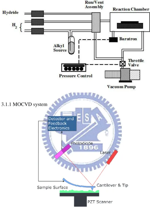
A reactor is a chamber made of a material that does not react with the chemicals
being used. It must also withstand high temperatures. This chamber is composed by
reactor walls, liner, a susceptor, gas injection units, and temperature control units.
Usually, the reactor walls are made from stainless steel or quartz. To prevent over
heating, cooling water must be flowing through the channels within the reactor walls.
Ceramic or special glasses, such as quartz, are often used as the liner in the reactor
chamber between the reactor wall and the susceptor. A substrate sits on a susceptor
which is at a controlled temperature. The susceptor is made from a material resistant
to the metalorganic compounds used; graphite is sometimes used. For growing
nitrides and related materials, a special coating on the graphite susceptor is necessary
to prevent corrosion by ammonia (NH3) gas. (Fig3.1.1)
Gas inlet and switching system -- Gas is introduced via devices known as
'bubblers'. In a bubbler a carrier gas (usually nitrogen or hydrogen) is bubbled through
the metalorganic liquid, which picks up some metalorganic vapour and transports it to
the reactor. The amount of metalorganic vapour transported depends on the rate of
carrier gas flow and the bubbler temperature, and is usually controlled automatically
and most accurately by using a Piezocon type vapour control system. Allowance must
be made for saturated vapours.
Gas Exhaust and cleaning System -- Toxic waste products must be converted to
liquid or solid wastes for recycling (preferably) or disposal. Ideally processes will be
designed to minimize the production of waste products.
3.2 Transmission Electron Microscope (TEM), Atomic Force Microscopy(AFM)
and Scanning electron microscope (SEM)
1. Transmission Electron Microscope (TEM)
Transmission electron microscope is the pre-eminent method for determining dislocation’ and other crystallographic defects character and for performing chemical and crystallographic analysis of micrometer and smaller precipitates and other
microstructures. With the similar structure and more powerful function compared with
SEM, TEM offers the in-depth perspective of specimen characterizations.
Any TEM is a complex assembly of magnetic lenses, several apertures, a sample
holder and an image recording/viewing system. The objective lens forms a diffraction
pattern in the back focal plane with electrons scattered by the sample and gombines
them to generate an image in the image plane (1. intermediate image). Thus,
diffraction pattern and image are simultaneously present in the TEM. It depends on
the intermediate lens which of them appears in the plane of the second intermediate
image and magnified by the projective lens on the viewing screen. Switching from
changing the strength of the intermediate lens. In imaging mode, and objective
aperture can be inserted in the back focal plane to select one or more beams that
contribute to the final image (BF, DF, HRTEM). In selected area electron diffraction
(SAED), an aperture in the plane of the first intermediate image defines the region of
which the diffraction is obtained.
In the bright field (BF) mode of the TEM, an objective aperture is placed in the
back focal plane of the objective lens which allows only the direct beam to pass. In
this case, mass-thickness and diffraction contrast contribute to image formation: thick
areas, areas in which heavy atoms are enriched, and crystalline areas appear with dark
contrast. In spite of the useful information obtainable from BF images, it should be
mentioned that the interpretation of contrast is often impeded since these phenomena
occur simultaneously.
In dark field (DF) images, one or more diffracted beams are allowed to pass the
objective aperture. The direct beam is blocked by the aperture. In contrast to the direct
beam, the diffracted beam has interacted strongly with the specimen, and often very
useful information is present in DF images, e.g., about planar defects, stacking faults
or particle size.
To obtain lattice images, a larger objective aperture has to be selected that allows
interference of the diffracted beams with the direct beam (phase contrast). If the point
resolution of the microscope is sufficiently high and a suitable sample oriented along
a zone axis, then high-resolution TEM (HRTEM) images are obtained. In many cases,
the atomic structure of the specimen can directly be investigated by HRTEM.
The incident parallel electron wave interacts elastically while passing through the
specimen, and the resulting modulations of its phase and amplitude are present in the
electron wave leaving the specimen. The wave here, the object exit wave o(r), thus
contains the information about the object structure. The objective lens performs 1.
The Fourier Transform (Fourier analysis) that creates the diffraction pattern of the
object in the back focal plane and 2. the inverse Fourier Transform (Fourier synthesis)
that makes the interference of the diffracted beams back to a real space image in the
image plane (lattice image).
2. Atomic force microscopy (AFM)
Atomic force microscopy (AFM) or scanning force microscopy (SFM) is a very
high-resolution type of scanning probe microscopy, with demonstrated resolution of
fractions of a nanometer, more than 1000 times better than the optical diffraction limit.
The precursor to the AFM, the scanning tunneling microscope, was developed by
Gerd Binnig and Heinrich Rohrer in the early 1980s at IBM Research - Zurich, a
Gerber invented the first atomic force microscope (also abbreviated as AFM) in 1986.
The first commercially available atomic force microscope was introduced in 1989.
The AFM is one of the foremost tools for imaging, measuring, and manipulating
matter at the nanoscale. The information is gathered by "feeling" the surface with a
mechanical probe. Piezoelectric elements that facilitate tiny but accurate and precise
movements on (electronic) command enable the very precise scanning. In some
variations, electric potentials can also be scanned using conducting cantilevers. In
newer more advanced versions, currents can even be passed through the tip to probe
the electrical conductivity or transport of the underlying surface, but this is much
more challenging with very few groups reporting reliable data.
The AFM consists of a cantilever with a sharp tip (probe) at its end that is used
to scan the specimen surface. (Fig3.2.1) The cantilever is typically silicon or silicon
nitride with a tip radius of curvature on the order of nanometers. When the tip is
brought into proximity of a sample surface, forces between the tip and the sample lead
to a deflection of the cantilever according to Hooke's law. Depending on the situation,
forces that are measured in AFM include mechanical contact force, van der Waals
forces, capillary forces, chemical bonding, electrostatic forces, magnetic forces (see
magnetic force microscope, MFM), Casimir forces, solvation forces, etc. As well as
specialized types of probe (see scanning thermal microscopy, photothermal
microspectroscopy, etc.). Typically, the deflection is measured using a laser spot
reflected from the top surface of the cantilever into an array of photodiodes. Other
methods that are used include optical interferometry, capacitive sensing or
piezoresistive AFM cantilevers. These cantilevers are fabricated with piezoresistive
elements that act as a strain gauge. Using a Wheatstone bridge, strain in the AFM
cantilever due to deflection can be measured, but this method is not as sensitive as
laser deflection or interferometry.
If the tip was scanned at a constant height, a risk would exist that the tip collides
with the surface, causing damage. Hence, in most cases a feedback mechanism is
employed to adjust the tip-to-sample distance to maintain a constant force between the
tip and the sample. Traditionally, the sample is mounted on a piezoelectric tube, that
can move the sample in the z direction for maintaining a constant force, and the x and
y directions for scanning the sample. Alternatively a 'tripod' configuration of three
piezo crystals may be employed, with each responsible for scanning in the x,y and z
directions. This eliminates some of the distortion effects seen with a tube scanner. In
newer designs, the tip is mounted on a vertical piezo scanner while the sample is
being scanned in X and Y using another piezo block. The resulting map of the area s
The AFM can be operated in a number of modes, depending on the application.
In general, possible imaging modes are divided into static (also called contact) modes
and a variety of dynamic (or non-contact) modes where the cantilever is vibrated.
3. Scanning electron microscope (SEM)
The scanning electron microscope (SEM) is a type of electron microscope that
images the sample surface by scanning it with a high-energy beam of electrons in a
raster scan pattern. (Fig. 3.2.3)The electrons interact with the atoms that make up the
sample producing signals that contain information about the sample's surface
topography, composition and other properties such as electrical conductivity.
The types of signals produced by an SEM include secondary electrons,
back-scattered electrons (BSE), characteristic X-rays, light (cathodoluminescence),
specimen current and transmitted electrons. Secondary electron detectors are common
in all SEMs, but it is rare that a single machine would have detectors for all possible
signals. The signals result from interactions of the electron beam with atoms at or near
the surface of the sample. In the most common or standard detection mode, secondary
electron imaging or SEI, the SEM can produce very high-resolution images of a
sample surface, revealing details about less than 1 to 5 nm in size. Due to the very
narrow electron beam, SEM micrographs have a large depth of field yielding a
structure of a sample. This is exemplified by the micrograph of pollen shown to the
right. A wide range of magnifications is possible, from about 10 times (about
equivalent to that of a powerful hand-lens) to more than 500,000 times, about 250
times the magnification limit of the best light microscopes. Back-scattered electrons
(BSE) are beam electrons that are reflected from the sample by elastic scattering. BSE
are often used in analytical SEM along with the spectra made from the characteristic
X-rays. Because the intensity of the BSE signal is strongly related to the atomic
number (Z) of the specimen, BSE images can provide information about the
distribution of different elements in the sample. For the same reason, BSE imaging
can image colloidal gold immuno-labels of 5 or 10 nm diameter which would
otherwise be difficult or impossible to detect in secondary electron images in
biological specimens. Characteristic X-rays are emitted when the electron beam
removes an inner shell electron from the sample, causing a higher energy electron to
fill the shell and release energy. These characteristic X-rays are used to identify the
composition and measure the abundance of elements in the sample.
3.3 Photoluminescence
Photoluminescence, a powerful and breakless analysis technology, can reveal the
band structure and the carrier transportation behaviors in a material. Moreover, the
carrier transportation, lifetime, etc. of the nano-material will be shown in the
photoluminescence spectrum.
Photoluminescence is a process in which a chemical compound absorbs photons
(electromagnetic radiation), transitioning to a higher electronic energy state, and then
radiatives photons back out, returning to a lower energy state. The period between
absorption and emission is extremely short, on the order of 10 nanoseconds. Light is
directed on a sample, where it is absorbed and imparts excess energy into the material
in a process called photo-excitation. The luminescence arising from photo-excitation
is called photoluminescence (PL). The intensity and spectral content of the
photoluminescence is a direct measurement of various important material properties.
Fig 3.3.1 shows the schematic setup of PL system with He-Cd laser operating at
30mW at the wavelength of 325nm.
Typically, the process of the luminescence consists of three steps, which is (1)
excitation, (2) thermal equilibrium and (3) recombination. Through thermal
equilibrium, electron-hole pairs (e-h pairs) generated by incident light recombine and
create photon. In the energy band gap, impurities and defects form a variety of energy
levels, whose corresponding energy produces radiation through radiative
Fig 3.1.1 MOCVD system
Fig. 3.2.3 Schematic diagram of an SEM
Chapter 4 Optical properties of a-plane In
0.2Ga
0.8N/GaN multiple
quantum wells grown on nanorod GaN templates
4.1 Introduction
InGaN-based semiconductors have been used intensively as light emitting diodes
(LEDs) and laser diodes (LDs) for their wide band gap through visible to near
ultraviolet light spectra [28]. However, the quantum efficiency is reduced in
conventional c-plane polar structure, which is due to the existent of the built-in
electric field. This built-in electric field would result in decreasing the oscillation
strength of the electron-hole pairs and reducing the carrier recombination rate. Recent
studies of InGaN/GaN multiple quantum wells (MQWs) demonstrate that it is
possible to eliminate such polarization fields along the nonpolar orientation.However,
the difficulty to utilize nonpolar GaN is not a suitable substrate for heteroepitaxial
a-plane GaN growth. In general, the threading dislocation (TD) density of
~3×1010cm−2 and a basal stacking fault density of ~3.5×105 cm−1 were commonly
observed in a-plane GaN grown on r-plane sapphire. [29] The TDs in GaN act as
nonradiative recombination centers which are responsible for poor internal quantum
efficiency (IQE). In this thesis, we investigated optical properties of a-plane
InGaN/GaN multiple quantum wells with improved GaN template.
InGaN/GaN MQWs. In section 2, we describe the method how we prepared the
samples and had successfully grown five samples with different crystal quality of
GaN template. In section 3, we knew the IQEPL (room temperature intensity/ low
temperature intensity) and the activation energy fitting result from temperature
dependent PL measurement. In section 4, the polarization-dependent PL revealed that
the degree of polarization and we simulated strain effect with polarization. In section
5, power dependent PL revealed nonpolar InGaN/GaN MQWs is free from QCSE. In
section 6, we present a comparative study of the internal quantum efficiency (IQE)
and fit nonradiative coefficient from results.
4.2 Samples preparation and growth
The process of nanorod epitaxial lateral overgrowth (NRELOG) is schematically
shown in Fig. 4.2.1. First, a 1.7-um-thick a-plane GaN layer was grown on r-plane
sapphire by metal-organic chemical vapor deposition (MOCVD). Then, a SiO2 film
with a 200 nm thickness and a Ni film with a 10 nm thickness were deposited in
sequence to act as the etching mask. Subsequently, the thermal annealing treatment
was utilized to obtain nanoscale Ni masks. The diameter of the Ni mask is 300–500
nm and the mask density is estimated to be around 6×108cm2 as shown in Fig. 4.2.2.
The Ni masks exhibit a random distribution with arbitrary geometries. After that, the
(RIE) /inductively coupled plasma etching (ICP) until the height of these nanorods is
0.2, 0.7, 1.2, 1.7 um and 0 um (without nanorod). The etchants for RIE were SF6 and
Ar, and the etchants for ICP etching were Ar, BCl3, and Cl2. Then, the SiO2 films
were deposited on the nanorods. Since the etching rate of RIE is anisotropic (the
vertical etching rate is faster than horizontal etching rate), we can control the RIE
parameters to remove the SiO2 on top of a-plane nanorods and the top of nanorods
exhibit the flat a-plane surface. Because the nanorods were fabricated via Ni masks,
the shape and homogeneities of nanorods was similar to that of Ni masks. Finally, the
GaN regrowth was performed on the nanorod template by MOCVD.
Figures 4.2.3 show the 9 um2 atomic force microscopy (AFM) images of the
as-grown sample and the NRELOG samples, respectively. These samples were grown
under the same growth conditions (the growth temperature, pressure, and V/III ratio
were 1180 °C, 200 mbar, and 800–900, respectively). Compared with the as-grown
sample, the NRELOG samples apparently had the superior surface quality and less
surface pits when the depth of nanorod is deeper. It is believed to be originated from
the TD terminations with the surface. [29] Therefore, the less surface pits show the
possibility of dislocation reduction. The rms roughness of the NRELOG sample was
approximately 1.39 nm in 1.7um sample, which was smaller than that of the as-grown
Then, as shown in Fig. 4.2.4, 6 pairs of 60 Å -thick InGaN well / 180 Å -thick GaN
barrier MQW were grown on all templates. We prepared five groups of MQW with
the same condition. The anisotropic strain within nonpolar structures results in more
complex Poisson ratio. Although there are many researches about a-plane structures,
the Indium composition of the a-plane InGaN/GaN MQWs still could not be
calculated precisely. The X-Ray th / 2th scan of a-plane InGaN / GaN MQWs
analysis confirmed that the Indium compositions are about 20%. Micro-structural
characterization was carried out using the plan-view TEM images of the a-plane GaN
film regrown on 1.7-μm-height nanorods in Fig.4.2.5 and the average TDD was
estimated to be 1×109 cm-2, which was about 1~2 orders magnitude lower than that
in as-grown GaN (3×1010 cm-2). Typical bright-field cross-sectional TEM image of
the a-plane In0.2Ga0.8N/GaN MQWs on 1.7-μm-height nanorods was shown in Fig.
4.2.6.
4.3 Temperature dependent photoluminescence a-plane InGaN/GaN MQWs
We want to know the optical properties of a-plane InGaN/GaN MQWs grown on
nanorod GaN templates including the carrier confinement and the activation energy, we
performed the temperature-dependent photoluminescence from 40 to 300K.
Fig. 4.3.1 shows the evolution of PL spectra as a function of temperature for the
partial phase segregation and composition inhomogeneity would result in exciton
localization within some indium-rich regions. [30] The low-energy peak existed from
40 to 300 K referred to the signal come from MQWs, and the high-energy peak merged
at high temperature referred to the signal from shallow localized states.
The decrease of PL intensity with increasing temperature is observed. Thermal
quenching PL intensity with increasing temperature is a general phenomenon in
semiconductor nanostructure which is caused by carriers thermalization from the
radiative recombination centers or/and localized states to the nonradiative
recombination centers or/and delocalized states. Temperature-dependent PL was
utilized to investigate the quantum efficiency of the grown samples. In general, the
temperature-induced quenching of luminescence involves the thermal activation of
excitons to nonradiative defect states. [31] In other words, a slower intensity decline
with the temperature increasing means a lower defect density in the grown sample.
The normalized integrated PL intensity ratio obtained at 40 and 300 K
IPL(300k)/IPL(40k) in Table 4.3.1 could represent the IQE of the InGaN/GaN MQWs
samples. The IQE obtained from IPL(300k)/IPL(40k) value are sequent 0.1 (0um), 0.15
(0.2um), 0.27 (0.7um), 0.28 (1.2um) and 0.35 (1.7um). As we can see, the internal
quantum efficiency increased with the depth of nanorod template and had an
times increase compared to that of the as-grown GaN. The reduction in the TD
density in case of NRELOG samples as compared to as-grown samples can contribute
to the enhancement in the quantum efficiency. [32]
Fig. 4.3.2 shows the normalized integrated PL intensity of InGaN/GaN MQWs
emission as a function of 1000/T for the as-grown sample and the NRELOG samples.
It has been studied that the carrier could receive activation energy to thermalize from
the potential minima, the radiative or localized centers, to nonradiative or delocalized
centers as the temperature is increased. [33] Therefore, it is expected that the deeper
localization with better confinement should have larger activation energy. In order to
further verify that, the experimental temperature-dependent PL data were fitted by
Arrhenius equation to investigate the carrier behavior during the thermal processes,
[34]
I (T) = I0/ [1+a*exp (-Ea/KBT) +b*exp (-Eb/KBT)] Eq. (4.3.1)
where I(T) is the temperature-dependent PL intensity, I0 is the PL intensity at 40 K, Kb
is Boltzmann’s constant, A and B are the rate constants, and Ea and Eb are the activation energies for two different nonradiative channels, which can be
distinguished for the high temperature and low temperature region. [35] The fitted
activation energy of the five samples is listed in Table 4.3.2. As expected, the
when nanorod depth is 1.7um. The trend of the activation energy is consistency with
the internal quantum efficiency. It is believed that the carrier confinement would
improve when the nanorod depth is deeper. Because the quality of a-plane GaN films
was improved by using nanorod GaN template and it was better when nanorod depth
was deeper.
In addition, the evolution with temperature of the peak shift of MQWS peak
energy for the five samples investigated here is given in Fig. 4.3.3, where the peak
positions at 40 K are the reference. The peak shift of PL varies as a function of
temperature from 40 to 300 K and exhibits a continuous redshift.
4.4 In-plane polarization effect of a-plane InGaN/GaN MQWs emission
In nonpolar InGaN/GaN MQWs, the anisotropic biaxial strain attributed to the
low symmetry of its structures. In this section, we performed a polarization-dependent
PL measurement at 300 K to investigate the effects of GaN templates on the
polarization characteristics. The PL measurement was excited using the 325 nm
He-Cd laser and a rotational polarizer was placed in front of the entrance slit of the
spectrometer. The schematic of our experimental setup for the PL measurement is
shown in Fig. 4.4.1. We varied the polarization in [11-20] a-plane from 0o, parallel to
the m-axis (E⊥C), 0° to 90°, parallel to the c-axis (E//C). The coordinate system used
Fig. 4.4.2(a) shows the room temperature polarization-dependent PL spectra with
nanorod GaN templates varied from 0um to 1.7um and the polarization angles from 0o
to 90o divided by 15o. In order to understand the emission intensity on polarization
angels, the symmetric of normalized PL intensity versus the polarization degree from
0o to 360o was also illustrated in Fig. 4.4.2(b).
The polarization degree ρ is defined as
ρ= (I⊥-I║) / (I⊥+I║) Eq. (4.4.1)
, where I⊥ and I// are PL intensities represented for E⊥C and E//C. The polarization degree ρ of our samples are sequent 85, 81, 65, 60 and 53 % for 0, 0.2, 0.7, 1.2 and 1.7um nanorod depth at 300 K. Here, only the low energy peak of InGaN/GaN
MQWs, which was dominant in the luminescence mechanism from 300 K, was
discussed and the results were listed in Table 4.4.1. The experiment results show that the polarization degree and peak energy shift (△E) was decreasing when the etching depth of nanorod was increasing. In addition, we also investigated the effect of
different nanorod depth on the polarization degree.
In Fig. 4.4.3, the polarization ratio was plotted as the function of etching depth of
nanorod. From data of the polarization ratio and peak energy shift, we could infer that
the strain, carrier density and scattering are reasons. And strain might be the main
contact area with sapphire as regrowth. In addition, the strain would be relaxed [12]
with increasing nanorod depth. We have known that the crystal quality of a-plane
GaN films was improved by using epitaxial lateral overgrowth on a nanorod GaN
template by AFM and TEM. We think the compressive strain of a-plane InGan/GaN
MQWs would be alleviated with nanrod depth. And we prove our thoughts through
simulation; the voids in GaN template were more when the nanorod depth is deeper,
so the effect of scattering was more obvious.
According to simulation, the injection carrier density and the strain would affect
polarization degree. From Eq. (4.4.2),
Eq. (4.4.2)
Eq. (4.4.3)
the generation rate was identical at the same power in our experiments. The fitting
results in Chapter 4.6, we knew that the value of A1.7um was the smallest than other
samples when B was the same. So the injection carrier density was the biggest in 1.7um
and was the smallest in 0 um. Fig 4.4.4 Simulated polarization degree with different
injection carrier density of In0.25Ga0.75N/GaN MQWs at 300K. PL spectrum simulated
as a function of x’-polarized and y’-polarized of In0.25Ga0.75N/GaN MQWs at 300K
varied strain from 1 time to 2 times in Fig. 4.4.5 and we supposed the injection current
density was 5×1018 cm-3. The polarization degree and peak energy shift (△E) was ) /( ) 1 ( ) /( ) 1 ( R l A lhv P R A hv P
G laser spot laser spot
2 Bn An R
increasing when the strain was increasing. The trend of simulation in Fig. 4.4.6 is
consistency with the experiment.
4.5 Nonpolar characteristics of a-plane InGaN/GaN MQWs
In conventional c-plane polar structure, the built-in field with the MQWs would
lead to band tilting. If the photo-genarated carriers were injected into the MQWs, the
built-in electric field could be screened and result in a blue-shift of PL energy peak
[36]. As we mentioned above, the useful approach for reducing the built-in electric
field is to grown MQWs along the nonpolar direction. In this section, we performed
the power dependent photoluminescence to realize the built-in field influence on our
samples.
The power dependent photoluminescence was demonstrated by using He-Cd
laser operated at 325 nm. The excitation power increased from 5uW to 35 mW. Fig.
4.5.1 shows the PL spectra as a function of excitation power for our five samples with
different nanorod depth at room temperature. As our previous work on c-plane
MQWs, increasing the Indium composition would result in larger PL peak blue-shift
as the In composition was increased, which is known to due to larger built-in electric
field [37]. On the contrary, the wavelength un-shift was observed of our five samples
during the power-dependent PL measurement as shown in Fig. 4.5.2. The unchanged
samples along nonpolar a–plane directions.
In addition, we also investigated the excitation power dependence on
luminescence intensity. Fig. 4.5.2 shows the relation between excitation power
density and the integrated PL intensity. The results were fitting based on the relation
I~Pα where I is the integrated PL intensity, P is the excitation power density and α is
the power index. In the case of c-plane MQWs, the superlinear relation (α>1) due to
decreasing nonradiative recombination with photo-injected carriers has been observed
[36]. The α factors of our samples were approximate 1. The linear relation of these four samples (α~1) indicated the nonradiative channels saturate and radiative recombination predominates. Therefore, it can be concluded that the QCSE was
absent in our samples.
4.6 Measuring internal quantum efficiency and fitting nonradiative
recombination coefficient of GaInN/GaN MQWs with different dislocation
densities
PL was measured with changing excitation power density at 300 and 20 K on the
same point. [38] A 325 nm He-Cd laser was used to excite all samples consistently,
which have nominally the same structure, except for the nanorod depth of GaN
template. The excitation power density at the sample surface was changed from 0.05
samples at 20 and 300 K. Curves are normalized by the peak value at 20 K for both
samples. We assume peak PL efficiency at 20K is 100% and correspond to IQE curve
for both samples at 20 and 300 K plots in Fig. 4.6.1. At 300 K, the 1.7um sample
shows a higher efficiency than the as-grown sample and the IQE of a-plane
InGaN/GaN MQWs are approximately 39% (1.7um), 30% (1.2um), 26% (0.7um),
16% (0.2um), and 13%(0um), respectively. In the present experiment, a 325 nm
He-Cd laser was used and this excites above the GaN bandgap energy. Therefore,
there is a possibility that the carrier excited at the GaN barrier layer contributed to PL,
especially at LT. [39] This makes measured IQE at RT somewhat higher than the
actual case. Fortunately, this condition was not obvious in our data at 20k (Fig 4.6.2)
and 300k (Fig 4.5.1).
Next, we present a theoretical model. [40] The three main carrier-recombination
mechanisms in a bulk semiconductor are Shockley–Read–Hall nonradiative
recombination, expressed as An, bimolecular radiative recombination Bn2, and Auger
nonradiative recombination Cn3, where A, B, and C are the respective recombination
coefficients and n is the carrier concentration. Auger recombination affects LED
efficiency only at very high excitation; In our experiments, the generation rate and the
IQE at steady state can be expressed as
Eq. (4.6.1) 3 2 Cn Bn An R G total Bn Bn IQE 2 2