國 立 交 通 大 學
電子工程學系 電子研究所
博 士 論 文
低臨界電壓雙金屬閘極
金氧半電晶體製作技術之研發
The Investigation of Low Threshold Voltage
Dual Metal Gate MOSFET Technology
研 究 生:鄭存甫
指導教授:荊鳳德 博士
低臨界電壓雙金屬閘極金氧半電晶體製作技術之研發
The Investigation of Low Threshold Voltage Dual Metal Gate
MOSFET Technology
研 究 生:鄭存甫 Student: Chun-Fu Cheng
指導教授:荊鳳德 博士 Advisor: Dr. Albert Chin
國立交通大學
電子工程學系電子研究所
博士論文
A Dissertation
Submitted to Department of Electronics Engineering & Institute of Electronics College of Electrical and Computer Engineering
National Chiao Tung University in Partial Fulfillment of the Requirements
For the Degree of Doctor of Philosophy
In
i
低臨界電壓雙金屬閘極金氧半電晶體製作技術之研發
研究生:鄭存甫 指導教授:荊鳳德 博士
國立交通大學
電子工程學系暨電子研究所博士班
摘要
隨著互補式金氧半電晶體(C-MOSFETs)的持續微縮,複晶矽閘極在 45 奈米以下技 術將遭遇到許多本質上的限制,包括高電阻率、硼穿隧和複晶空乏。除此之外,高介電 常數介電質也將導入製程以取代傳統二氧化矽或氮氧化矽介電質。然而,有研究指出複 晶矽閘極跟高介電常數介電質間會有費米能階栓(Fermi-level pinning)效應。因此,金屬 閘極顯然是解決以上問題的良好選擇。使用金屬閘極必須符合適當功函數、熱穩定、製 程兼容性和更佳的元件效能等需求。在本論文研究中,包含全金屬矽化(FUSI)閘極和低 溫處理純金屬閘極這二種類型雙金屬閘極製程技術的研究。 首先,我們先微縮等效氧化層厚度(EOT)從 1.6 奈米到 1.2 奈米,並使用矽化鉿閘極 這方面的研究。我們從臨界電壓(Vt)和電子移動率來觀察發現等效氧化層厚度 1.2 奈米之 氮氧化鑭鉿N 型金氧半電晶體,在使用低功率數高溫穩定的矽化鉿閘極有良好的效能。 自我對準以及閘極優先的矽化鉿/氮氧化鑭鉿 N 型金氧化電晶體擁有簡單的高溫全金屬矽化處理以及兼容於現今極大型積體電路整合(VLSI)生產線等優點。 在接下來的研究,我們使用與之前類似的矽化銥全金屬矽化製程。我們可以從極低 的漏電、良好的電洞移動率、1000 度 C 高溫穩定性中看出良好的矽化銥/氮氧化鑭鉿 P 型金氧化電晶體元件整合特性。然而,在等效氧化層厚度1.2 奈米下卻觀察到不佳的平 帶電壓和高臨界電壓。因此,我們目標是發展出一種新的製程技術來解決這個問題。 為了研究平帶電壓下滑的現象,我們首先比較使用相同矽化銥閘極在不同等效氧化 層厚度下的平帶電壓。最後我們研發出一個新的高功率數銥/氧化鑭鉿P 型金氧半電晶 體,使用低溫處理淺接面製程。自我對準銥/氧化鑭鉿P 型金氧半電晶體的優點為適當 的5.3 電子伏特之等效金屬功率數、+0.05 伏特之低臨界電壓、在電場為-0.3 MV/cm 下 90 cm2/V-s 之高電洞移動率以及 20 mV 之微小偏壓溫度不穩定性(在 85 度 C,10 MV/cm 以及一小時的條件下)。本實驗結果擁有 1.2 奈米等效氧化層厚度、和簡單的自我對準製 類似以及閘極優先之極大型積體電路製程,比之前發表的金屬閘極高介電常數介電質P 型金氧半電晶體結果不相上下或是較佳。 最後我們也試著同時降低 N 型金氧半電晶體的製程溫度,使用鉿/氧化鑭鉿固態擴 散製程。我們研究兩種不同的固態擴散製程。結果發現使用低功函數鉿閘極的氧化鑭鉿 N 型金氧半電晶體在 1.2 奈米等效氧化厚度下,在臨界電壓以及移動率的觀點都有良好
iii
然而當氧化層厚度持續的微縮,1000 度 C 的摻雜活化處理變得越來越關鍵。在我們的
研究中,使用低溫製程技術可以解決平帶電壓下滑以及不需要的高臨界電壓。因此在我
The Investigation of Low Threshold Voltage Dual Metal Gate MOSFET
Technology
Student: Chun- Fu Cheng Advisor: Dr. Albert Chin
Department of Electronics Engineering
& Institute of Electronics
National Chiao Tung University
ABSTRACT
With the continuous scaling trend of complementary metal-oxide-semiconductor field
effect transistors (C-MOSFETs) technology, poly-silicon gates encounter several inherent
drawbacks beyond the 45 nm technology node including high resistivity, boron penetration
and poly-depletion. In addition, high-κ gate dielectrics have also been introduced to replace
v
stability, process compatibility and better device performance. In this dissertation, two novel
dual metal gate process technologies including fully silicided (FUSI) gates and
low-temperaure-processed pure metal gate were investigated.
At first, scaling the effective oxide thickness (EOT) from 1.6 nm to 1.2 nm using HfSix
gates was studied. We have found good performance in terms of threshold voltage (Vt) and
mobility for Hf0.7La0.3ON n-MOSFETs at 1.2 nm EOT using a low work-function and
high-temperature-stable HfSix gate. The self-aligned and gate-first HfSix/HfLaON
n-MOSFETs have the advantages of simple high temperature FUSI processing and
compatibility with current very large scale integration (VLSI) lines.
In the following study, similar FUSI process using IrSix gates was also investigated.
Good device integrity of Ir3Si/HfLaON p-MOSFETs is shown by the very low leakage current,
good hole mobility and 1000oC thermal stability. However, poor flat band voltage (Vfb) and
high Vt is observed at 1.2 nm EOT. As a result, we aimed to develop a new process
technology to solve this problem.
In order to study the origin of Vfb roll-off phenomenon, we compared the Vfb of Ir3Si
gates under different EOT. Finally, we develop a new process technology of high
work-function Ir/HfLaO p-MOSFETs using low-temperature-processed shallow junction. The
merits of self-aligned Ir/HfLaO p-MOSFETs are the proper φm-eff of 5.3 eV, low Vt of +0.05 V,
& 1 hr). These results are comparable with or better than the previous reported data for
metal-gate/high-κ p-MOSFETs, with small 1.2 nm EOT, similar simple self-aligned and
gate-first process for VLSI IC fabrication.
Finally, we also tried to decrease the process temperature of n-MOSFET by Hf/HfLaO
using solid phase diffusion (SPD). Two different SPD shallow junctions were studied. We
have found good performance in terms of Vt and mobility for HfLaO n-MOSFETs at 1.2 nm
EOT using a low work-function Hf gate. The self-aligned and gate-first Hf/HfLaO
n-MOSFETs have the advantages of ≤900oC low processing temperature and good device
performance for VLSI fabrication.
In conclusion, metal silicide FUSI processes have the advantage of proper φm-eff, high
temperature stable. However, as the continuous scaling of oxide thickness, the thermal budge
of 1000oC dopant activation process has become more critical. In our study, the Vfb roll-off
and unwanted high Vt can be solved by low temperature process technology. As a result, it is
necessary to further decrease the process temperature for both n- and p-MOSFETs in our
vii
Acknowledgement
First of all, I would like to thank my advisor Prof. Albert Chin for his fruitful
instructions and enthusiastic discussions for my dissertation. I am also grateful to all members
in ED633 group, including those seniors, D. S. Yu, H. L. Kao, C. H. Lai, C. H. Wu and B. F.
Hung, for their help in my study; those classmates, G. T. Lin, C. F. Li, Y. Y. Tseng and J. M.
Lai, for their accompany in my graduate school life; especially N. C. Su, S. G. Shen and W. L.
Huang for their assistance in experiments.
Moreover, I am appreciative of the financial and equipment supports from National
Science Council, Nano Facility Center of NCTU and National Nano Device Laboratory. I am
also grateful to those who ever assisted this work.
Finally, I greatly appreciate the endless encouragement and spiritual support of my
family and my dear girl friend Miss Ling-Ru Guo. Without them, I can’t finish this
Contents
Abstract (in Chinese)……….i
Abstract (in English)………... iv
Acknowledgement………...vii
Contents………..viii
Table Captions………..xi
Figure Captions………...xii
Chapter 1 Introduction 1.1 Metal Gate Electrodes……….…1
1.1.1 Classification of Metal Gate Materials………..1
1.1.2 Work Function………3
1.2 High-κ materials………..3
1.3 Metal Gate High-κ Strategy……….5
ix
2.3 Result and Discussion……….17
2.4 Conclusion………..19
Chapter 3 HfLaON p-MOSFETs Using High Work Function Ir3Si Gate 3.1 Introduction……….26
3.2 Experimental Procedure………..27
3.3 Result and Discussion……….27
3.4 Conclusion………..28
Chapter 4 High Work-Function Ir/HfLaO p-MOSFETs Using Low-Temperature- Processed Shallow Junction 4.1 Introduction……….35
4.2 Experimental Procedure………..36
4.3 Result and Discussion……….37
4.3.1 Vfb roll-off issue at thinner EOT………..37
4.3.2 Low temperature shallow junction formed by SPD………...39
4.3.3 Device characteristics of low temperature SPD formed Ir/HfLaO p-MOS…………...40
4.4 Conclusion………..42
Chapter 5 Very Low Vt Hf/HfLaO n-MOSFETs Using Self-Aligned Low Temperature Shallow Junction 5.1 Introduction……….53
5.2 Experimental Procedure………..54
5.3 Result and Discussion……….54
5.3.1 Low temperature shallow junction formed by SPD………...54
5.3.2 Device characteristics of low temperature SPD formed Hf/HfLaO n-MOS…………..55
5.4 Conclusion………..56
Chapter 6 Summary and Conclusions………..69
References...71
Vita...89
xi
Table Captions
Chapter 1 Introduction
Table 1-1 Comparison of different Metal Gate High-κ Strategy………8
Chapter 2 HfLaON n-MOSFETs Using Low Work Function HfSix Gate
Table 2-1 Comparison of device parameters for metal-gate/high-κ n-MOSFETs………20
Chapter 4 High Work-Function Ir/HfLaO p-MOSFETs Using Low-Temperature-
Processed Shallow Junction
Table 4-1 Comparison of important device parameters among metal-gate/high-κ
p-MOSFETs………..41
Chapter 5 Very Low Vt Hf/HfLaO n-MOSFETs Using Self-Aligned Low Temperature
Shallow Junction
Table 5-1 Comparison of important device parameters among metal-gate/high-κ
Figure Captions:
Chapter 1 Introduction
Fig. 1-1 The common elements in periodic table. The elements were marked with p, n and
m according to its work function near the valence band, conduction band and
mid-gap of silicon energy band, respectively………9
Fig. 1-2 Work Function variation versus atomic number………..10
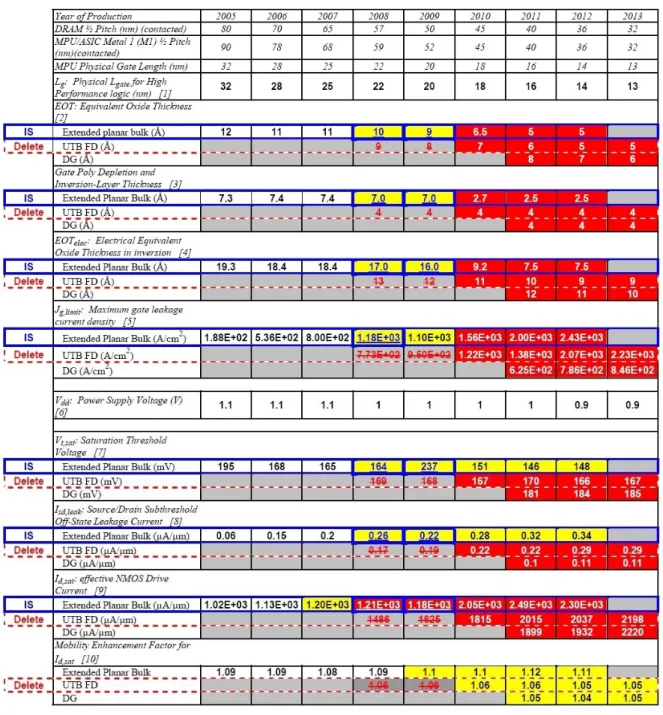
Fig. 1-3 High-performance logic technology requirements (the international technology
roadmap for semiconductors:2006 update)………..11
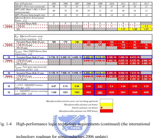
Fig. 1-4 High-performance logic technology requirements (continued) (the international
technology roadmap for semiconductors:2006 update)………...12
Fig. 1-5 Grazing incident XRD spectra of HfLaON with NH3 plasma after different RTA
annealing. In contrast to the HfLaO case, the HfLaON stays amorphous state after
1000oC RTA……….13
Fig. 1-6 The band offset of popular high-κ materials………14
xiii
Fig. 2-1 C-V characteristics of the HfSix/Hf0.7La0.3ON n-MOS capacitors, after a 1000oC
RTA. The inserted figure is a Vfb-EOT plot………..21
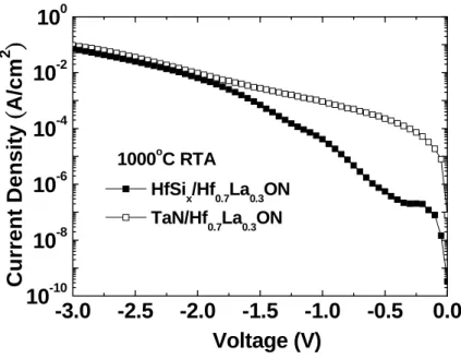
Fig. 2-2 J-V characteristics of the HfSix/Hf0.7La0.3ON n-MOS capacitors, after a 1000oC
RTA………..22
Fig. 2-3 The Id-Vd characteristics of the HfSix/Hf0.7La0.3ON n-MOSFETs………...23
Fig. 2-4 The Id-Vg characteristics of the HfSix/Hf0.7La0.3ON n-MOSFETs………...24
Chapter 3 HfLaON p-MOSFETs Using High Work Function Ir3Si Gate
Fig. 3-1 C-V characteristics of Ir3Si/HfLaON and TaN/HfLaON capacitors respectively,
after a 1000oC RTA………..30
Fig. 3-2 J-V characteristics of Ir3Si/HfLaON and TaN/HfLaON capacitors respectively,
after a 1000oC RTA………..31
Fig. 3-3 The Id-Vd characteristics of the Ir3Si/HfLaON p-MOSFETs………32
Fig. 3-4 The Id-Vg characteristics of the Ir3Si/HfLaON p-MOSFETs………33
Fig. 3-5 The hole mobility vs. effective electric field for the Ir3Si/HfLaON p-MOSFETs...34
Chapter 4 High Work-Function Ir/HfLaO p-MOSFETs Using Low-Temperature-
Processed Shallow Junction
Fig. 4-1 C-V characteristics of (a) Ir3Si/HfLaON p-MOSFETs after 1000oC RTA and (b)
Ir/HfLaO p-MOSFETs after 850oC RTA. The C-V characteristics were measured at
Fig. 4-2 Charge pumping current as a function of gate pulse frequency for 1000oC
processed HfLaON and 850oC processed HfLaO………45
Fig. 4-3 J-V characteristics of p+
/n junction formed by (a) SiO2/Ga SPD at 900oC RTA and control B+ implantation at 1000oC RTA; (b) SiO2/Ni/Ga SPD at 550~850oC RTA.46
Fig. 4-4 SIMS profile of Ga and Ni/Ga-silicide p+
/n junction formed by SPD………47
Fig. 4-5 (a)J-V and (b)Vfb-EOT characteristics of Ir/HfLaO p-MOS after 850oC RTA…..48
Fig. 4-6 The Id-Vd characteristics of Ir/HfLaO p-MOSFET using Ga or NiGa-silicide S/D.49
Fig. 4-7 The Id-Vg characteristics of Ir/HfLaO or Ir3Si/HfLaON p-MOSFETs………50
Fig. 4-8 The extracted hole mobility from Id-Vg characteristics of Ir/HfLaO or
Ir3Si/HfLaON p-MOSFETs……….51
Fig. 4-9 The ∆Vt shift of Ir/HfLaO p-MOSFETs stressed at 85oC and 10 MV/cm for 1
hour………..52
Chapter 5 Very Low Vt Hf/HfLaO n-MOSFETs Using Self-Aligned Low Temperature
Shallow Junction
Fig. 5-1 Variation Rs of NiAl (insert), H3PO4 spin SPD and As+ implant with RTA
xv
Fig. 5-3 XRD of HfLaO after 600oC and 900oC 30 sec RTA. Amorphous structure w/o
crystallization is still preserved and important for BTI………61
Fig. 5-4 (a) J-V of n+/p junction with NiAl Schottky contact. Although Rs<10 Ω/sq, the
leakage and n are poor. (b) J-V of n+
/p junctions made by H3PO4 spin SPD at 850 and 875oC RTA. The leakage and n are similar to those for the As+ implant and
1000oC RTA case………..62
Fig. 5-5 C-V of HfLaO n-MOS with Ir/TaN/Hf and TaN gates after 875 and 900oC RTAs.
Data from a quantum-mechanical C-V simulation are included………..63
Fig. 5-6 J-V of HfLaO n-MOS with Ir/TaN/Hf and TaN gates, after 875 and 900oC RTAs..64
Fig. 5-7 Vfb-EOT for TaN and Hf gates. Effective work-functions are 4.3 and 4.1 eV…….65
Fig. 5-8 The Id-Vd characteristics of the Hf/HfLaO n-MOSFETs……….66
Fig. 5-9 The Id-Vg characteristics of the Hf/HfLaO n-MOSFETs……….67
Fig. 5-10 The electron mobility vs. effective electric field for the Hf/HfLaO and
Chapter 1
Introduction
1.1 Metal Gate Electrodes
As traditional poly-silicon (poly-Si) gated metal-oxide semiconductor field effect
transistors (MOSFETs) scales, the additional series capacitance due to poly-Si depletion
becomes an increasingly large fraction of the total gate capacitance [1.1]-[1.13]. Besides,
boron penetration from the poly-Si gate will also degrade the performance of the transistors.
In order to overcome these problems, metal gate electrodes was used to be a practical way to
eliminate poly-gate depletion and boron penetration [1.1]-[1.8]. In addition, metal gates also
have the potential to reduce sheet resistance of gate electrodes. Metal electrodes with suitable
work functions and sufficient physical and electrical stability are being widely investigated to
solve these problems.
1.1.1 Classification of Metal Gate Materials
Metal gate materials are generally classified into four major types including pure metals,
2
(Ev) relative to locations of elements [1.14]. Elements in column IIIB, IVB VB such as Ti,
Y, Hf, Ta and Lanthanide series have n-type work functions; elements in column VIB and
part elements in column VIIB such as Mo and W have mid-gap work functions; elements in
column VIIB such as Rh, Ir, Ni, Pd and Pt tend to have p-type work functions. N-type
elements are chemically reactive. As a result, a capping metal layer such as TaN is
necessary to prevent possible reaction during thermal process. P-type elements are
relatively inert and can sustain the high temperature process. However, the chemical inertia
results in the difficulties in patterning and poorness in adhesion.
(2) Metallic alloys:
Typically, metallic alloys are binary alloys consist of n-type metal and p-type
metal/mid-gap metals, such as Ta-Pt alloys, Ta-Ru alloys and Hf-Mo alloys [1.15-1.17].
The work function is determined by the atomic composition. Alloys with higher n-type
metal content have a lower work function. On contrary, alloy with higher p-type metal
content have a higher work function.
(3) Metal silicides:
Metal react with silicon to form metal silicides. The popular metal silicide candidates
are hafnium silicide, molybdenum silicide, tungsten silicide, nickel silicide, cobalt silicide,
platinum silicide and Iridium silicide. The merit of metal silicide gates is the compatibility
metal gate materials.
(4) Other metal nitrides/carbides/oxides
Metals react with nitrogen/carbon/oxygen to form metal nitrides/carbides/oxides
which are more chemically stable on dielectrics than pure metal. The work function can be
adjusted by the nitrogen/carbon/oxygen composition and metal nitrides/carbides/oxides
phase, but the tunable range is not wide enough to be used for both n- and p-MOSFETs. In
addition, an obvious drawback is the high resistivity.
1.1.2 Work Function
Metal work functions (φm) are shown in Fig. 1-2 and they play an important role for
metal-gate/high-κ C-MOSFETs. The preferred work function of the metals are ~5.2 eV for
p-MOSFETs and ~4.1 eV for n-MOSFETs. Recently, lots of metal or metal-nitride materials
have been widely researched and successfully intergraded in advanced C-MOSFETs, such as
TiN, TaN, Pt, Mo and Ir [1.1]-[1.13]. However, it has been found that thermal annealing of the
metal gates at high temperature results in mid-gap values for some metal gate candidates
[1.18]. Therefore, the Fermi-level pinning effect needs to be avoided by selecting suitable
4
consideration of the required properties of gate dielectrics indicates that the key guidelines for
selecting an alternative gate dielectric are [1.19]-[1.24]:
(1) Permittivity
(2) Band gap
(3) Band alignment to silicon
(4) Thermodynamic stability
(5) Film morphology
(6) Interface quality
(7) Compatibility with the current or expected materials to be used in processing for
CMOS devices
(8) Reliability
Many dielectrics appear favorable in some of these areas, but very few materials are
promising with respect to all of these guidelines. Specifically, a dielectric constant (κ) ~25 is
required to satisfy the requirements for CMOS gate dielectrics leading out to years beyond
2010. Similar or larger values are required for dielectrics used in embedded dynamic random
access memory (DRAM) cells and radiofrequency (RF) coupling capacitors. The material
must also respond positively to a series of other demands relating to such effects as lack of
interactivity with the Si substrate, low leakage currents, low interface state density, high
oxide increases significantly because direct tunneling is the primary conduction mechanism in
down-scaling CMOS technologies. Therefore, the engineering of high- κ gate dielectrics have
attracted great attention and played an important role in VLSI technology.
According to the ITRS (International Technology Roadmap for Semiconductor) [1.25],
the suitable gate dielectrics must have value more than 8 for 50-70 nm technology nodes and
that must be more than 15 when the technology dimension less than 50 nm. Figs. 1-3 and 1-4
show the evolution of CMOS technology requirements. Oxy-nitrides (SiOxNy) have been
introduced to extend the use of SiO2 in production but eventually it has to be replaced by a
high-κ material, such as Ta2O5, TiO2, HfO2, ZrO2, Al2O3, La2O3 or mixtures of them or
metal-oxide-silicates of the mentioned compounds. However, most metal oxides will have the
characteristics of crystallization at elevated temperature which cause devices generate
non-uniform leakage distribution and give large statistical variation for nano-meter devices
across the chip. Materials such as HfLaON can still preserve its amorphous structure up to
1000oC as Fig. 1-5 shows. Fig. 1-6 shows the summaries of the κ value and band offset for
popular high-κ dielectric candidates. To predict the M-N thermal stability, in Fig.1-7 we show
6
Single Metal Single Dielectric (SMSD), Dual Metal Single Dielectric (DMSD), Single Metal
Dual Dielectric (SMDD) and Dual Metal Dual Dielectric (DMDD). Table 1-1 lists pros and
cons of different metal gate high-κ strategy. In a metal gate technology, one approach
employs a metal with mid-gap work function for both n- and p-MOSFETs. The drawbacks are
that the threshold voltages would be too large for a reasonable channel doping, and
counter-doping the channel to alleviate this problem degrades short-channel and turn-off
characteristics [1.26], [1.27]. Hence, an approach analogous to the established dual-poly-Si
gate technology, i.e., a dual-metal gate technology, would be preferred. The major challenge
is to find two metals with suitable work functions and a way to integrate them into a CMOS
process.
1.4 Overview of Dissertation
At first, scaling the effective oxide thickness (EOT) from 1.6 nm to 1.2nm using HfSix
gates was studied. In the following study, similar FUSI process using IrSix gates was also
investigated. However, poor effective metal work function (φm-eff) and high threshold voltgage
(Vt) is observed at 1.2nm EOT. As a result, we aimed to develop a new process technology to
solve this problem.
In order to study the origin of flat-band voltage (Vfb) roll-off phenomenon. We
compared the Vfb of IrSix gates under different EOT. Finally, we develop a new process
shallow junction. Finally, we also tried to decrease the process temperature of n-MOSFET by
Hf/HfLaO using solid phase diffusion (SPD). Two different Solid phase diffusion (SPD)
shallow junctions were studied. The self-aligned and gate-first Hf/HfLaO n-MOSFETs have
the advantages of ≤900oC low processing temperature and good device performance using a
8
Table 1-1 Comparison of different Metal Gate High-κ Strategy.
Pros Cons
SMSD 9 Simple process 8 Limited range of work function tuning 8 Metal/Dielectric interface problem 8 Poor Device performance
SMDD 9 Less complicated process step 9 Wider range of work function tuning 9 Good Device performance
8 Two dielectric deposition steps 8 Metal/Dielectric interface problem 8 Work function tuning range of dielectric
material is not as large as metal gates. DMSD 9 Less complicated process step
9 Wider range of work function tuning 9 Good Device performance
8 Two gate deposition steps
8 Metal/Dielectric interface problem DMDD 9 Widest range of work function tuning
9 Most Flexible in metal/dielectric selection 9 Good Device performance
8 Two dielectric deposition steps 8 Two gate deposition steps 8 Complex etching steps
IA 0
H IIA IIIA IVA VA VIA VIIA He
Li Be B C N O F Ne
Na Mg IIIB IVB VB VIB VIIB ┌─ VIIIB ─┐ IB IIB Al Si P S Cl Ar
N N N M M M M P M N K Ca Sc Ti V Cr Mn Fe Co Ni Cu Zn Ga Ge As Se Br Kr N N N M M M P P P N Rb Sr Y Zr Nb Mo Tc Ru Rh Pd Ag Cd In Sn Sb Te I Xe N N N M P M P P P M Cs Ba *La Hf Ta W Re Os Ir Pt Au Hg Tl Pb Bi Po At Rn Fr Ra +Ac Rf Ha Sg Ns Hs Mt 110 111 112 113 N N N N N N N N N N N N N *Lanthanide Series Ce Pr Nd Pm Sm Eu Gd Tb Dy Ho Er Tm Yb Lu +Actinide Series Th Pa U Np Pu Am Cm Bk Cf Es Fm Md No Lr
Fig. 1-1 The common elements in periodic table. The elements were marked with p, n and
m according to its work function near the valence band, conduction band and
10 0 10 20 30 40 50 60 70 80 90 100 0 1 2 3 4 5 6 Ir Pt Hf Tb Yb La Y Ec group-IA Ba Fr group-IIA Rb Be Li Cs Sr K Ca Al Mg Na W o rk Function (eV) Atomic Number Ev Lanthanide
Fig. 1-3 High-performance logic technology requirements (the international technology
12
Fig. 1-4 High-performance logic technology requirements (continued) (the international
20 30 40 50 60 2θ (Degree) In te n s it y
(
cps)
400oC 800oC 1000oCHfLaON with 3 min NH3 plasma
Fig. 1-5 Grazing incident XRD spectra of HfLaON with NH3 plasma after different RTA
annealing. In contrast to the HfLaO case, the HfLaON stays amorphous state after
14
20 30 40 50 60 70 80 0 200 400 600 800 1000 Metal-Oxide Metal-Nitride Metal-Carbide Bon d E n th al py ( KJ /mol) Atomic Number Ti Ta Hf La Yb Tb Ir Zr Si
Fig. 1-7 Bond enthalpy for M-O, M-N and M-C in the Periodic Table for thermal stability
prediction, with M-O>M-N>M-C in general. The bond enthalpy peaked at La, Hf
16
Chapter 2
HfLaON n-MOSFETs Using Low Work Function HfSi
xGate
2.1 Introduction
Metal gates and high-κ gate dielectrics are necessary for CMOSFETs at the 45 nm
nodes and beyond [2.1]-[2.15], to reduce the DC power consumption from the gate current
and continue the VLSI scaling. This poses a difficult technological challenge in that the large
threshold voltage (Vt) that results from Fermi-level pinning is opposite to the trend needed for
device scaling. To avoid this requires appropriate choices of the metal-gate work-function and
high-κ dielectric - to reduce the pinning to achieve the required low Vt. Previously, we have
shown that Fermi-level pinning can be reduced, even after surface plasma nitridation, by
adding La2O3 to HfO2, to produce the gate dielectric Hf0.5La0.5ON at 1.6 nm equivalent oxide
thickness (EOT). Thus, a relatively low Vt can be achieved with a conventional TaN gate
[2.15]. Here we report the use of a low work-function Fully Silicided (FUSI) HfSix gate for
Hf0.7La0.3ON n-MOSFETs, at a scaled EOT of 1.2 nm and reduced La composition of 30%.
This gate yields a more negative flat band voltage (Vfb) than does a TaN gate. The resulting
MOSFETs show a Vt of 0.18 V, a low leakage current of 9.2×10⁻⁴ A/cm2 at 1 V above Vfb and
1.2 nm EOT, with an electron mobility of 215 cm2/V-s. These devices can endure a rapid
2.2 Experimental procedure
We used the 4-inch p-type Si wafers in these experiments. After a standard RCA clean,
the Hf0.7La0.3O was deposited on Si wafers by physical vapor deposition. Then the Hf0.7La0.3O
surface was exposed to nitrogen plasma to form the Hf0.7La0.3ON gate dielectric. Amorphous
Si of 5 nm thickness was deposited on the Hf0.7La0.3ON followed by a PVD deposition of 20
nm thick Hf. To prevent Hf oxidation, a 30 nm thick Mo was subsequently deposited above
the Hf/Si/Hf0.7La0.3ON to form n-MOS capacitors. For n-MOSFETs, an additional 150 nm
thick amorphous-Si was deposited to avoid ion implantation damage through the gate. The n+
source-drain regions were formed by using a 35 KeV phosphorus ion implantation (at a
5×1015 cm-2 dose) followed by RTA activation at 1000oC for 5 sec. (Note that the FUSI HfSi x
gate was formed at a high RTA temperature, similar to Ir3Si[2.14], which is different from a
conventional low temperature salicide process.) For comparison, TaN gates were also
deposited on the Hf0.7La0.3ON to form the n-MOS capacitors. The fabricated devices were
characterized by C-V and I-V measurements using an HP4284A precision LCR meter and
HP4156 semiconductor parameter analyzer, respectively.
18
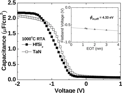
depletion – as formed by Hf deposition on thin 5 nm amorphous-Si at 1000oC RTA –
produces devices with a high capacitance density, close to those using a TaN gate. However,
the Vfb of the HfSix gate is more negative than for the TaN gate, which is needed for low Vt
operation. An EOT of 1.2 nm was found using a quantum-mechanical (QM) C-V simulation.
A low φm-eff of 4.33 eV was obtained from a Vfb-EOT plot for the HfSix/Hf0.7La0.3ON devices,
making them suitable for n-MOS applications. The leakage current of 9.2×10⁻⁴ A/cm2 (at 1 V
beyond Vfb) is ~5 orders of magnitude lower than that of SiO2 at a 1.2 nm EOT. This low
leakage current is due to the high-κ Hf0.7La0.3ON, highlighting the good thermal stability of
the HfSix/Hf0.7La0.3ON gate structure after a 1000oC RTA. The higher leakage current at low
voltages using TaN gate than that of HfSix may be due to the sputter-induced damage to
Hf0.7La0.3ON gate dielectric. Thus, both low φm-eff and low gate dielectric leakage current can
be achieved in HfSix/Hf0.7La0.3ON MOS capacitors.
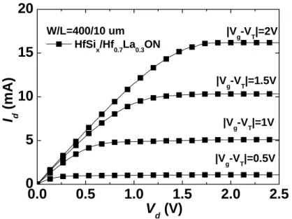
Figures 2-3 and 2-4 show the Id-Vd and Id-Vg transistor characteristics of the 1.2 nm EOT
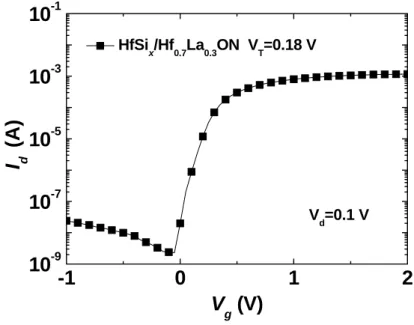
HfSix/Hf0.7La0.3ON n-MOSFETs. A small Vt of only 0.18 V was measured from the linear
Id-Vg plot - this is due to the low φm-eff of 4.33 eV found from the C-V measurements.
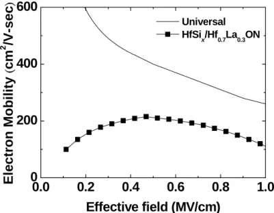
The electron mobility as a function of effective electric field for the HfSix/Hf0.7La0.3ON
n-MOSFETs is shown in Fig. 2-5, where the data was derived from measured Id-Vg curves.
High peak electron mobility of 215 cm2/V-s is obtained, at a small EOT of 1.2 nm. In Table 1
metal-gate/high-κ n-MOSFETs. The merits of the HfSix/Hf0.7La0.3ON n-MOSFETs are the
small EOT of 1.2 nm, low Vt of 0.18 V, good peak mobility of 215 cm2/V-s and simple
high-temperature FUSI processing.
2.4 Conclusion
We have found good performance in terms of Vt and mobility for Hf0.7La0.3ON
n-MOSFETs at 1.2 nm EOT using a low work-function and high-temperature-stable HfSix
gate. The self-aligned and gate-first HfSix/HfLaON n-MOSFETs have the advantages of
20
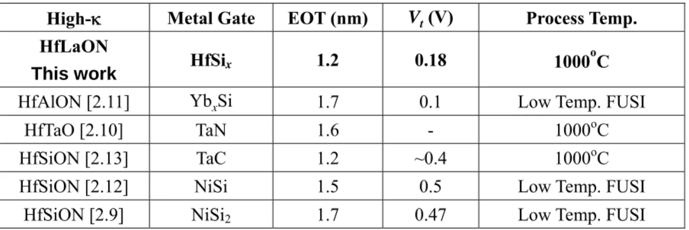
Table 2-1 Comparison of device parameters for metal-gate/high-κ n-MOSFETs.
High-κ Metal Gate EOT (nm) Vt (V) Process Temp. HfLaON
This work HfSix 1.2 0.18 1000
o
C
HfAlON [2.11] YbxSi 1.7 0.1 Low Temp. FUSI HfTaO [2.10] TaN 1.6 - 1000oC HfSiON [2.13] TaC 1.2 ~0.4 1000oC HfSiON [2.12] NiSi 1.5 0.5 Low Temp. FUSI
-2 -1 0 1 0.0 0.5 1.0 1.5 2.0 2.5 1000oC RTA HfSi x TaN Voltage (V) C a pac it a nce
(
µ F/cm 2)
Fig. 2-1 C-V characteristics of the HfSix/Hf0.7La0.3ON n-MOS capacitors, after a 1000oC
RTA. The inserted figure is a Vfb-EOT plot.
0 1 2 3 4 -1.0 -0.5 0.0 φm,eff = 4.33 eV Fl atb and V o lt age ( V ) EOT (nm)
22 -3.0 -2.5 -2.0 -1.5 -1.0 -0.5 0.0 10-10 10-8 10-6 10-4 10-2 100 1000oC RTA HfSix/Hf0.7La0.3ON TaN/Hf0.7La0.3ON Voltage (V) Cu rren t Den s it y
(
A/ cm 2)
Fig. 2-2 J-V characteristics of the HfSix/Hf0.7La0.3ON n-MOS capacitors, after a 1000oC
0.0
0.5
1.0
1.5
2.0
2.5
0
5
10
15
20
|V g-VT|=0.5V |Vg-VT|=1V |V g-VT|=1.5VI
d(mA)
V
d(V)
W/L=400/10 um HfSi x/Hf0.7La0.3ON |Vg-VT|=2V24
-1
0
1
2
10
-910
-710
-510
-310
-1 HfSi x/Hf0.7La0.3ON VT=0.18 VI
d(A)
V
g(V)
Vd=0.1 V0.0 0.2 0.4 0.6 0.8 1.0 0 200 400 600 Universal HfSix/Hf0.7La0.3ON El ect ron Mobi li ty ( cm 2 /V -sec ) Effective field (MV/cm)
Fig. 2-5 The electron mobility vs. effective electric field for the HfSix/Hf0.7La0.3ON
26
Chapter 3
HfLaON p-MOSFETs Using High Work Function Ir
3Si Gate
3.1 Introduction
According to the International Technology Roadmap for Semiconductors (ITRS), the
metal-gate/high-κ is the required technology for the future generation C-MOSFETs to reduce
the undesired large gate leakage current and continue the gate oxide scaling [3.1]-[3.11].
Recently, the HfSiON gate dielectric is a promising candidate beyond SiON with merits of
high κ value, low gate leakage current and similar amorphous structure after 1000oC RTA for
VLSI process. However, the lack of a high work function gate for HfSiON p-MOSFETs is the
challenge since only Ir (5.27 eV) and Pt (5.65 eV) in the Periodic Table [3.8] have the needed
work function larger than target 5.2 eV. The other problem of HfSiON is the relative lower κ
of 10~14 that causes limited scaling capability. In this paper, we developed the high
temperature stable Ir3Si/HfLaON p-MOSFET to address above issues. The novel HfLaON
dielectric can preserve the amorphous structure after 1000oC RTA and is similar to HfSiON
but with significantly higher κ value. Using high work-function Ir3Si gate electrode [3.8]-[3.9],
the p-MOSFETs show good device integrity of low leakage current of 1.8×10⁻⁵ A/cm2 at 1 V
above flat band voltage (Vfb), high hole mobility of 84 cm2/Vs and good 1000oC RTA thermal
better than the best reported metal-gate/high-κ p-MOSFETs [3.1]-[3.7].
3.2 Experimental procedure
Standard N-type Si wafers with resistivity 1~10 Ω-cm (1015-1016 cm-3 doping level)
were used in this study. After standard RCA clean, the HfLaO was deposited on N-type Si
wafers by PVD and post deposition anneal (PDA). The HfLaON was formed by applying NH3
plasma surface nitridation on HfLaO. Then 5 nm amorphous Si and 20 nm Ir was
subsequently deposited on HfLaON and RTA annealed at 1000oC for 5 sec to form the MOS
capacitors. For p-MOSFETs, additional thick TaN capping layer is added on Ir/Si/HfLaON to
prevent subsequent ion implantation penetration, where the IrxSi gate was formed during RTA.
After patterning, self-aligned B+ implantation was applied at 25 KeV and source-drain doping
was activated at 1000oC RTA for 5 sec. The fabricated p-MOSFETs were characterized by
C-V and I-V measurements.
3.3 Result and Discussion
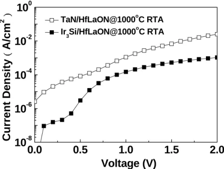
In Figures 3-1 and 3-2 we show the C-V and J-V characteristics of Ir3Si/HfLaON and
TaN/HfLaON capacitors respectively. For comparison, the characteristics of a capacitor with
28
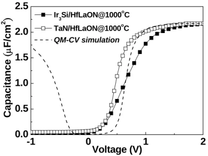
was found using a quantum-mechanical (QM) C-V simulation. However, unexpected Vfb
roll-off is observed which will cause high Vt and result in poor device performance. The
leakage current of 5.29×10⁻⁴ A/cm2 (at 1 V beyond V
fb) is ~5 orders of magnitude lower than
that of SiO2 at a 1.2 nm EOT. This low leakage current is due to the high-κ HfLaON,
highlighting the good thermal stability of the Ir3Si/HfLaON gate structure after a 1000oC
RTA. Thus, only low gate dielectric leakage current can be achieved in Ir3Si/HfLaON MOS
capacitors.
Figures 3-3 and 3-4 show the Id-Vd and Id-Vg transistor characteristics of the 1.2 nm EOT
Ir3Si/HfLaON p-MOSFETs. A high Vt of 0.25 V was measured from the linear Id-Vg plot - this
is due to the roll-off of Vfb that can be found from the C-V measurements.
The hole mobility as a function of effective electric field for the Ir3Si/HfLaON
p-MOSFETs is shown in Fig. 3-5, where the data was derived from measured Id-Vg curves.
High peak hole mobility of 86 cm2/V-s could still be obtained, at a small EOT of 1.2 nm. The
merits of the Ir3Si/HfLaON p-MOSFETs are the small EOT of 1.2 nm, good peak mobility of
215 cm2/V-s and simple high-temperature FUSI processing.
3.4 Conclusion
Good device integrity of Ir3Si/HfLaON p-MOSFETs is shown by the very low leakage
current, good hole mobility and 1000oC thermal stability. However, poor Vfb and high Vt is
30 -1 0 1 2 0.0 0.5 1.0 1.5 2.0 2.5 Voltage (V) Capaci tance
(
µ F/cm 2)
Ir3Si/HfLaON@1000oC TaN/HfLaON@1000oC QM-CV simulationFig. 3-1 C-V characteristics of Ir3Si/HfLaON and TaN/HfLaON capacitors respectively,
0.0
0.5
1.0
1.5
2.0
10
-810
-610
-410
-210
0Current Density
(A/cm
2 )Voltage (V)
TaN/HfLaON@1000oC RTA Ir3Si/HfLaON@1000oC RTAFig. 3-2 J-V characteristics of Ir3Si/HfLaON and TaN/HfLaON capacitors respectively,
32
-2.0
-1.5
-1.0
-0.5
0.0
0
2
4
6
8
10
|Vg-VT|=0.5V |Vg-VT|=1V |Vg-VT|=1.5VI
d(mA)
V
d(V)
Ir/HfLaO/n-Si W/L=400/10 µm Ir3Si/HfLaON |Vg-VT|=2V-2
-1
0
10
-910
-810
-710
-610
-510
-410
-310
-210
-1 Vd=-0.1 V W/L=400/10 µm Ir 3Si/HfLaON p-MOSFET VT=-0.25VI
d(A)
V
g(V)
34 -1.0 -0.8 -0.6 -0.4 -0.2 0.0 0 50 100 150 200 Universal Ir 3Si/HfLaON p-MOSFET@1000 o C µ eff (
cm
2/V
-sec
) Effective field (MV/cm)Chapter 4
High Work-Function Ir/HfLaO p-MOSFETs Using
Low-Temperature-Processed Shallow Junction
4.1 Introduction
To reduce the unwanted gate leakage current and continue the logic device evolution,
metal-gates and high-κ technology are required for C-MOSFETs used for 45 nm node and
beyond [4.1]-[4.19]. The major challenge for metal-gate/high-κ C-MOSFETs is the undesired
high threshold voltage (Vt); this is especially difficult for p-MOS requiring high effective
work-function (φm-eff) gate, since only Ir and Pt in the Periodic Table has the needed >5.2 eV
values [4.13]. Furthermore, Ir can be patterned by Reactive-Ion etching (RIE) [4.20]-[4.21]
but not the case for Pt, which makes Ir the very few choice for high φm-eff p-MOS. Previously,
we showed that the self-aligned Ir3Si/HfLaON p-MOSFET [4.15] has the required low Vt of
-0.1 V by using high φm-eff Ir3Si gate of 5.08 eV at 1.6 nm effective oxide thickness (EOT).
This is achieved even after 1000oC rapid thermal annealing (RTA) used for source-drain
36
diffused (SPD) shallow junction. This self-aligned and gate-first p-MOSFET showed proper
φm-eff of 5.3 eV, low Vt of +0.05 V, high mobility of 90 cm2/Vs at -0.3 MV/cm and small 85oC
negative bias-temperature instability (NBTI) of 20 mV at 10 MV/cm for 1 hr. Besides, the
achieved p+
/n contact junction depth is in the range of 9.6~20 nm and useful for sub-90 nm
regime [4.22]. In comparing with 1000oC RTA-annealed Ir3Si/HfLaON p-MOSFET, this
achieved good device integrity in Ir/HfLaO is attributed to the using novel low-temperature
(≤900oC) ultra-shallow junction process, where the reaction at high-κ interface decreases
exponentially followed by Arrhenius law. These results compare well with the best report
metal-gate/high-κ p-MOSFETs [4.1]-[4.19], with lower Vt, smaller EOT, similar simple
self-aligned and gate-first process for VLSI IC fabrication.
4.2 Experimental Procedure
Standard n-type Si wafers with resistivity of 1-10 Ω-cm were used in this study. After
regular RCA cleaning, the HfLaO was deposited on n-Si substrate by physical vaper
deposition (PVD) and post-deposition annealing (PDA). The La content in HfLaO is
controlled to be 50%. Then, 20 nm Ir and 150 nm TaN were deposited by PVD. After gate
patterning, the self-aligned 5 nm Ga or 10-nm-Ni/5-nm-Ga, covered with 100 nm SiO2,was
deposited for p-MOS, followed by 550~900oC RTA SPD. Finally, source-drain metal contact
was added to reduce the source-drain contact resistance in Ga doped case. For comparison,
cm-2 dose and followed by 1000oC RTA dopant activation, where the HfLaON was formed by
applying NH3 plasma surface nitridation on HfLaO. More detailed fabricateion process can be
found elsewhere [4.15]. The fabricated p-MOSFETs were characterized by
capacitance-voltage (C-V) and current-voltage (I-V) measurements using an HP4284A
precision LCR meter and an HP4156 semiconductor parameter analyzer, respectively.
4.3 Result and Discussion
4.3.1 Vfb roll-off issue at thinner EOT:
Figures 4-1(a) and 4-1(b) show the C-V characteristics of Ir3Si/HfLaON and Ir/HfLaO
p-MOSFETs after 1000oC and 850oC RTA, respectively. Although proper high Vfb is obtained
in Ir3Si/HfLaON p-MOS at 1.6 nm EOT, the Vfb is largely decreased with further
down-scaling the EOT to 1.2 nm. Here the 1.2 nm EOT is confirmed from the
quantum-mechanical (QM) C-V simulation. In sharp contrast, the Ir/HfLaO p-MOSFETs after
850oC RTA did not show such lower Vfb effect at thinner 1.2 nm EOT. Similar band-edge
work-function for p-MOS was also reported using Pt electrode [4.14]. It is important to notice
that the measured C-V curve of 1000oC RTA-annealed Ir3Si/HfLaON p-MOS is deviated from
38
interface oxide charges may come from the charged oxide vacancies and dangling bonds of
non-stoichiometric oxides (x<2) caused by unavoidable interface reaction and inter-diffusion:
x
x HfO
SiO HfO
Si+ 2⎯⎯→∆ + 2− (1)
Such reactions are possible at high temperature owing to the similar bond enthalpies of
800 and 802 kJ/mol for respective SiO2 and HfO2 [4.13]. Although such silicate formation can
be decreased by inserting interfacial SiO2, unfortunately this will increase the EOT and
degrade the required high κ value for achieving low leakage current.
To exam this assumption, we have measured the interface trap density (Dit) of gate
dielectrics with different RTA temperature. Figure 4-2 shows the measured charge-pumping
current as a function of frequency. Linear dependences of the current on frequency were
measured. The Dit of 9.7×1011 cm-2eV-1 was obtained for 1000oC RTA processed HfLaON
from Groeseneken’s formula [4.23], which decreases to only 3.6×1011 cm-2eV-1 for 850oC
RTA thermal-cycled HfLaO. Such decreased Dit is very important to improve the device
performance in following sections.
On the other hand, the Ir/HfLaO device failed completely at 1000oC, this is due to the
inevitable metal diffusion [4.17] of Ir into HfLaO at higher temperatures. Similar Ir diffusion
into HfO2 was reported and confirmed by SIMS measurement [4.2]. Although this metal
diffusion through oxide can be decreased by using surface nitrided HfLaON, it still cannot
we have developed a low temperature shallow junction process for high-κ p-MOSFETs.
4.3.2 Low temperature shallow junction formed by SPD:
Figures 4-3(a) and 4-3(b) show the J-V characteristics of p+
/n junctions formed by
SiO2/Ga and SiO2/Ni/Ga SPD, respectively. Good p+/n junction characteristics are obtained
using SiO2/Ga SPD at 900oC RTA with reasonable ideality factor and low leakage current
close to B+ implanted controlled sample at 1000oC RTA. However, this process has relatively
high sheet resistance of ~1050 Ω/sq. due to the ultra shallow junction of 9.6 nm at 1018 cm-3
concentration [4.24] shown in the Secondary Ion Mass Spectroscopy (SIMS) profile of Fig.
4-4. The improved ideality factor from 1.7 to 1.5 was obtained with increasing RTA time from
10 to 20 sec. This suggests the deeper junction to give better diode characteristics, which may
be related to the reduced residue Ga in the depletion region.
To further improve the sheet resistance, the Ni-silicide is used. The incorporate Ni into
Ga decreases the sheet resistance to only 10 Ω/sq., where good ideality factor and reverse
leakage current are also obtained. The degradation of Ni/Ga formed junction in both ideality
factor and leakage current at 850oC may be due to the deformation of NiSi. From the SIMS
40
4.3.3 Device characteristics of low temperature SPD formed Ir/HfLaO p-MOS:
Based on the above shallow junctions, we have fabricated the Ir/HfLaO p-MOSFETs.
The high-κ HfLaO was subjected to a PDA of 850oC RTA in nitrogen ambient to reduce the
oxide defects. Figures 4-5(a) and 4-5(b) are the J-V and Vfb-EOT characteristics of TaN/Ir on
HfLaO devices, respectively. Here different HfLaO thickness was used to extract the Vfb. At
1.2 nm EOT, low leakage current of 2.4×10⁻⁴ is obtained at 1 V for p-MOS capacitors.
However, the Ir/HfLaO p-MOS devices were failed after 1000oC RTA due to Ir metal
diffusion through high-κ [4.2]-[4.16]. Therefore, the decreasing temperature to ≤900oC is
vitally important to use the high work-function Ir electrode. A proper φm-eff of 5.3 eV is
obtained for Ir/HfLaO device that is close to the ideal required band edge value of 5.2 eV
used for p-MOSFETs.
Figure 4-6 shows the transistor Id-Vd characteristics as a function of |Vg-Vt| for Ir/HfLaO
p-MOSFETs with 900oC RTA-annealed SiO2/Ga SPD and 700oC RTA-annealed SiO2/Ni/Ga
contacts. For comparison, the Id-Vd characteristics of Ir3Si/HfLaON p-MOSFETs with B+
implant junction at 1000oC RTA are also shown for comparison. At 1.2 nm EOT, the
well-behaved Id-Vd curves of these p-MOSFETs show good transistors performance using the
SPD junctions.
Figure 4-7 shows the Id-Vg characteristics of Ir/HfLaO and Ir3Si/HfLaON p-MOSFETs.
at 1.2 nm EOT. This is consistent with the large φm-eff of 5.3 eV from the Vfb-EOT plot shown
in Fig. 4-5(b). For Ir3Si/HfLaON p-MOSFETs, the Vt of -0.25V is obtained. This is due to the
Vfb roll-off shown in Fig. 1(a) that is attributed to the charged oxide vacancies in eq. (1) and
higher Dit value measured by charge-pumping current caused by higher 1000oC RTA.
Figure 8 shows the extracted hole motility versus gate electric field from the measured
Id-Vg characteristics for Ir/HfLaO and Ir3Si/HfLaON p-MOSFETs using SPD and B+
implanted junctions at 1.2 nm EOT. High peak hole mobility of 90 at -0.3 MV/cm and 86
cm2/V-s at -0.33 MV/cm is obtained for Ir/HfLaO and Ir3Si/HfLaON p-MOSFETs
respectively, which is comparable with the published data in the literature [1]-[19]. For
Ir3Si/HfLaON device, the sub-threshold swing (SS) is 81 mV/dec. For Ir/HfLaO with Ga/Ni
SPD case, a smaller SS of 74 mV/decade is obtained that is is close to the reported value of
LaO-capped HfSiON [4.19]. The improved SS is related to the measured lower Dit value
shown in Fig. 4-2.
The reliability is an important factor of high-κ MOSFETs. We have measured the NBTI
as shown in Fig. 4-9, under the condition of 10 MV/cm bias for 1 hr at 85oC. Here the stress
42
Table 4-1 summarizes and compares the important device parameters of
metal-gate/high-k p-MOSFETs. The merits of self-aligned Ir/HfLaO p-MOSFETs with SPD
shallow contact junction are the proper φm-eff of 5.3 eV, low Vt of +0.05 V, high mobility of 90
cm2/V-s at -0.3 MV/cm, and small BTI of 20 mV (85oC, 10 MV/cm & 1 hr). These results are
comparable with or better than the best reported data for metal-gate/high-κ p-MOSFETs, with
small 1.2 nm EOT, similar simple self-aligned and gate-first process for VLSI IC fabrication.
4.4 Conclusion
Good device performance of Ir/HfLaO p-MOSFETs is shown by the high φm-eff of 5.3
eV, low Vt of +0.05 V, shallow junction of 9 or 20 nm, high hole mobility of 90 cm2/V-s at
-0.3 MV/cm, and small BTI <20 mV (85oC, 10 MV/cm & 1 hr) with advantage of self-aligned
Table 4-1 Comparison of important device parameters among metal-gate/high-κ p-MOSFETs.
High-κ Metal-Gate EOT (nm) φm-eff (eV) Vt (V) Process Temp. Mobility (cm2/Vs) This work HfLaO Ir 1.2 5.3 +0.05 ≤850 o C SPD 90 Chapter 3 HfLaON Ir3Si 1.2 5.0 -0.25 1000 o C 86 HfLaON [4.15] Ir3Si 1.6 5.08 -0.1 1000oC 84 HfAlON [4.16] IrxSi 1.7 4.9 -0.29 950oC 80 HfSiON [4.11] Ni31Si12 1.5 ~4.8 -0.4 Low Temp. FUSI ~70
HfSiON [4.9] NiSiGe 1.3 - -0.5 Low Temp. FUSI 70 HfSiON [4.6] Ni3Si 1.7 4.8 -0.69 Low Temp. FUSI 65
44 -1 0 1 2 0.0 0.5 1.0 1.5 2.0 2.5 Voltage (V) Capaci tance
(
µ F/cm 2)
Vfb roll off1.2 nm EOT low freq. QM-CV simulation 1.6 nm EOT (a) -1 0 1 2 0.0 0.5 1.0 1.5 2.0 2.5
TaN 900oC Low Freq. QM C-V simulation
Voltage (V) Capaci tance ( µ F/ cm 2 )
TaN/Ir 850oC Low Freq. QM C-V simulation
(b)
Fig. 4-1 C-V characteristics of (a) Ir3Si/HfLaON p-MOSFETs after 1000oC RTA and (b)
Ir/HfLaO p-MOSFETs after 850oC RTA. The C-V characteristics were measured at 500 kHz.
10
310
410
510
610
710
-810
-710
-610
-510
-4Cha
rge
-p
umping c
u
rr
e
nt
(
A
)
Frequency (Hz)
HfLaO @ 850oC D it=3.6x10 11 cm-2.eV-1 HfLaON @ 1000oC D it=9.7x10 11 cm-2.eV-1 W/L=400/10 µm t r=tf=50 ns Vr=50 mVFig. 4-2 Charge pumping current as a function of gate pulse frequency for 1000oC
46
-2
-1
0
1
2
10
-610
-510
-410
-310
-210
-110
010
1Current Density
(A/
c
m
2 )Voltage (V)
Ga diffusion + RTA 900οC 10 sec n~1.7 900οC 20 sec n~1.5 B+ implantation 25 keV & 5x1015 cm-2 1000oC 5 sec n~1.4 (a) -2 -1 0 1 2 10-6 10-5 10-4 10-3 10-2 10-1 100 101 Cu rren t Den s it y(
A/cm 2)
Voltage(V) Ga/Ni +RTA 550oC 700oC n~1.36 850oC n~1.8 (b) Fig. 4-3 J-V characteristics of p+/n junction formed by (a) SiO2/Ga SPD at 900oC RTA and control B+ implantation at 1000oC RTA; (b) SiO2/Ni/Ga SPD at 550~850oC RTA.
0
50
100
10
1510
1610
1710
1810
1910
2010
2110
2210
232
3
4
5
Conce
n
tr
at
ion
(
cm
-3)
Depth (nm)
Ga RTA 900oC Ni RTA 700oC Ga RTA 700oC SiSi concentration
(
10
22cm
-3)
Ga:Ni co-diffusion Ga diffusion NiGa silicideFig. 4-4 SIMS profile of Ga and Ni/Ga-silicide p+
48 0.0 0.5 1.0 1.5 2.0 10-9 10-7 10-5 10-3 10-1 101 Ir 900oC Ir 1000oC fail Gate Current ( A/cm 2 ) Voltage (V) Ir 850oC (a)
0
1
2
3
4
-1.5
-1.0
-0.5
0.0
0.5
1.0
1.5
2.0
2.5
Ir/HfLaO processed under 850oC RTA for 30 sec
V
fb(V
)
Effective Oxide Thickness (nm)
φm,eff
=5.3 eV
(b)
-2.5
0
-2.0
-1.5
-1.0
-0.5
0.0
2
4
6
8
10
|V g-VT|=0.5V |V g-VT|=1V |V g-VT|=1.5VI
d(mA)
V
d(V)
Ir/HfLaO/n-Si W/L=400/10 µm Ga Ir/HfLaO formed @ 900oC Ga:Ni Ir/HfLaO formed @ 700oC B+implant Ir3Si/HfLaON|V
g-VT|=2V
50
-2
-1
0
1
10
-910
-810
-710
-610
-510
-410
-310
-210
-1 Vd=-0.1 V W/L=400/10 µmGa Ir/HfLaO p-MOSFET formed @ 900o
C VT=0.05V
Ga:Ni Ir/HfLaO p-MOSFET formed @ 700o C V
T=0.05V
B+
implant Ir3Si/HfLaON p-MOSFET VT=-0.25V
I
d(A)
V
g(V)
-1.0 -0.8 -0.6 -0.4 -0.2 0.0 0 50 100 150 200 Universal
Ga Ir/HfLaO p-MOSFET formed @ 900oC
Ga:Ni Ir/HfLaO p-MOSFET formed @ 700oC
B+implant Ir 3Si/HfLaON p-MOSFET@1000 oC µ eff (
cm
2/V
-sec
) Effective field (MV/cm)Fig. 4-8 The extracted hole mobility from Id-Vg characteristics of Ir/HfLaO or
52 100 101 102 103 104 10-1 100 101 102 103 | ∆ V t | ( m V ) Time (sec)
HfLaO p-MOSFET formed @ 900oC
HfLaON p-MOSFET formed @ 1000oC,
10 MV/cm and 85oC 50 mV
Chapter 5
Very Low V
tHf/HfLaO n-MOSFETs Using Self-Aligned Low Temperature
Shallow Junction
5.1 Introduction
Both metal gate and high-κ gate dielectric are needed to reduce the DC power
consumption and gate depletion to continue the VLSI scaling trend, [5.1]-[5.12]. However,
one of the difficult challenges for metal-gate/high-κ MOSFET is the large threshold voltage
(Vt) by Fermi-level pinning that is opposite to scaling trend. To overcome this problem, low
and high work-function metal-gates are required to reduce the pinning effect. Previously, we
have reported the HfSix gate on HfLaON has low effective work-function (φm-eff) of 4.33 eV
[5.12] and useful for n-MOS. For n-MOSFET, the novel TaC gate has shown low φm-eff
[5.1]-[5.2]. However, the Full Silicidation (FUSI) gate [5.3]-[5.5], [5.8]-[5.13] for n-MOS is
still needed to develop, which is due to the inherent advantage of the process compatibility
with current poly-Si gate CMOS technology. In this chapter, we used the similar method of
54
850oC. These results indicate the potential application for metal-gate/high-κ n-MOSFETs.
5.2 Experimental procedure
We used the 4-inch p-type Si wafers in these experiments. After a standard RCA clean,
the HfLaO was deposited on Si wafers by physical vapor deposition (PVD). Then Hf of 20
nm thickness was deposited on the HfLaO by PVD. To prevent Hf oxidation, a 50 nm thick
TaN and 20 nm thick Ir were subsequently deposited above the Hf/HfLaO to form n-MOS
capacitors. Then, NiAl-silicide Schottky contact for sub-45-nm node was made [5.15], or
self-aligned H3PO4 was spun deposited, transformed to P2O5 at 200oC and SPD at 850~900oC
RTA. Such wet H3PO4 spray and doping processes are used for commercial Si solar cell
manufacture. Finally, source-drain metal contacts were added. For comparison,
HfSix/HfLaON n-MOSFET using As+ 35 KeV ion implantation (at a 5×1015 cm-2 dose)
followed by RTA activation at 1000oC for 5 sec were also fabricated. The fabricated devices
were characterized by C-V and I-V measurements using an HP4284A precision LCR meter
and HP4156 semiconductor parameter analyzer, respectively.
5.3 Result and Discussion
5.3.1 Low temperature shallow junction formed by SPD
Fig. 1 shows the variation Rs of NiAl (insert), H3PO4 spin SPD and As+ implant with
RTA condition. Data for the 1 keV As+ implant and 1020oC RTA are from [5.16]. For NiAl
case, very low Rs ~10 Ω/sq. could be achieved after 450~650oC RTA. For H
compared with As+ implant with 1020oC RTA condition, H
3PO4 spin SPD at 850oC has comparable Rs compared with Xj of 29 nm As+ implant with 1020oC RTA. Moreover, H3PO4
spin SPD at 875~900oC has lower Rs compared with Xj of 29 nm As+ implant with 1020oC
RTA. In order to further check the reason of relative low Rs, we measured phosphorus SIMS
profile for H3PO4 spin SPD. The Xj data from [5.16] are also included for comparison. A USJ
Xj of 23 or 35 nm was measured by SIMS after 850 or 875oC RTA – this is better than that for
a 1 keV As+ implant and spike RTA at the same Rs [5.16]. This is due to the free from
defect-assisted diffusion caused by As+ implant damage. This ≤900oC process temperature is
important for HfLaO in preserving its amorphous structure at 900oC, as Fig. 5-3 shows,
without using the nitrided HfLaON, which reduces the possible pinning at metal-gate/high-κ
interface. The amorphous structure of HfLaO at 900oC is better than crystallized HfO2 for
achieving good BTI, by avoiding charge trapping at poly-HfO2 grain boundaries.
Figs. 5-4 (a) and 5-4(b) show the J-V of n+
/p junctions. Although the NiAl-silicide
Schottky contact has an n of 1.9, the self-aligned H3PO4 spin process improves n to 1.4, gives
a 10X smaller leakage and a low Rs. As a result, we finally choose the self-aligned H3PO4 spin
56
temperature to ≤900oC is vital for choosing proper φm-eff pure metal gate electrode.
Furthermore, we have also plotted the Vfb-EOT in Fig. 5-7 and proper φm-eff of 4.1 eV is
obtained for Hf/HfLaO n-MOS.
The Id-Vd, Id-Vg characteristics of Hf/HfLaO n- MOSFETs are shown in Figs. 5-8 and
5-9, respectively. Good transistor characteristics, high drive current and low Vt of 0.03 V, are
measured.
The µeff-E characteristics of Hf/HfLaO n- MOSFETs is derived from Id-Vg
characteristics and is shown in Fig. 5-10. High electron mobility of 243 cm2/Vs is also
observed. The improved mobility, compared with 1000oC RTA HfSix/HfLaON n-MOSFET, is
consistent with lower charged vacancies associated with interfacial reactions. Table 5-1
compares various metal-gate/high-κ n-MOSFET data.
The merits of self-aligned Hf/HfLaO n-MOS with SPD USJ are proper φm-eff of 4.1 eV,
low Vt of 0.03 V and high mobility of 243 cm2/Vs. Our results are comparable with or better
than the best reported data for metal-gate/high-κ n-MOSFET, with a small 1.2 nm EOT, and
using a self-aligned and gate-first process.
5.4 Conclusion
We have found good performance in terms of Vt and mobility for HfLaO n-MOSFETs
at 1.2 nm EOT using a low work-function Hf gate. The self-aligned and gate-first Hf/HfLaO