國 立 交 通 大 學
電子工程學系 電子研究所碩士班
碩 士 論 文
一個用來改善形變通道 N 型金氧半場效電晶體
熱載子可靠度的方法
A Novel Approach to Improve Hot Carrier
Reliability of Strained-Channel NMOSFETs
研 究 生:黃健銘
指導教授:黃調元 博士
林鴻志 博士
一個用來改善形變通道 N 型金氧半場效電晶體
熱載子可靠度的方法
A Novel Approach to Improve Hot Carrier
Reliability of Strained-Channel NMOSFETs
研 究 生
:
黃健銘 Student
:Jian-Ming Huang
指導教授 : 黃調元 博士 Advisors :Dr. Tiao-Yuan Huang
林鴻志
博士
Dr. Horng-Chih Lin
國 立 交 通 大 學
電子工程學系 電子研究所碩士班
碩 士 論 文
A Thesis
Submitted to Department of Electronics Engineering & Institute of Electronics College of Electrical Engineering and Computer Science
National Chiao-Tung University in Partial Fulfillment of the Requirements
for the Degree of Master of Science
in
Electronic Engineering September 2006
一個用來改善形變通道 N 型金氧半場效電晶體
熱載子可靠度的方法
研究生 : 黃健銘 指導教授 : 黃調元 博士
林鴻志 博士
國立交通大學
電子工程學系 電子研究所碩士班
摘要
在本研究中,我們探討了使用薄緩衝層對於具有形變通道的 n-型深次微米電 晶體的性能影響與可靠度分析。我們實驗發現,在氮化矽沉積前先沉積一層薄緩 衝層(thin buffer layer)並不會使元件性能變差,這是使用薄緩衝層的優點之 一。而沉積氮化矽覆蓋層時所帶來的熱預算(thermal budget)雖然可以降低界面 的缺陷與減少逆短通道效應,然而卻會使多晶矽空乏現象變嚴重。在本研究中, 我們分別探討了兩種緩衝層材質: 四乙氧基矽烷(TEOS)氧化矽與多晶矽。我們發 現在形變元件中氫含量的多寡是影響元件可靠度最主要的因素。使用四乙氧基矽 烷(TEOS)氧化矽緩衝層可以減緩沉積氮化矽的過程中氫擴散至閘極介電層的情 形。另一方面,由於在沉積多晶矽緩衝層的過程中是使用含有氫的矽甲烷(SiH4) 先驅物(precursor),所以多晶矽緩衝層沒有像四乙氧基矽烷(TEOS)緩衝層一樣佳的阻隔效果。當元件含有氮化矽覆蓋層來增進其驅動電流時,熱載子退化效應會 被嚴重地劣化,然而我們也證實:在氮化矽沉積前先沉積一層緩衝層,可以有效 改善熱載子退化效應。
A Novel Approach to Improve Hot Carrier
Reliability of Strained-Channel NMOSFETs
Student : Jian-Ming Huang Advisors : Dr. Tiao-Yuan Huang
Dr. Horng-Chih Lin
Department of Electronics Engineering and Institute of Electronics
National Chiao Tung University, Hsinchu, Taiwan
Abstract
In this work, the effect of a thin buffer layer inserted between the gate and a SiN capping layer on the performance and reliability of deep-submicron n-channel MOS transistors with strained channel was studied. It is found that the insertion of a thin buffer layer would not degrade the device performance, which is important for the adoption of the approach to the mainstream ULSI manufacturing. The thermal budget associated with the deposition of the SiN capping layer could reduce the amount of interface states and alleviate the reverse short-channel effect, although the poly-depletion effect becomes worse. More importantly, we found that hydrogen species is the primary culprit for aggravated reliabilities in strained devices. Two types of buffer
buffer layer could effectively block the diffusion of hydrogen species contained in the SiN layer into the channel region. On the other hand, poly-Si buffer layer does not depict the same blocking effect as TEOS, owing to the use of the H-containing precursor (e.g. SiH4) in the deposition step. Hot-electron degradation is adversely affected when the SiN layer is deposited over the gate. The effectiveness of the inserted buffer layer for alleviating the hot-carrier degradation of devices is clearly demonstrated: when a buffer layer is capped prior to the SiN deposition, although still worse than the control ones, significant improvement over that without the buffer could be obtained.
誌 謝
很高興完成了這份碩士論文,在碩班兩年中,讓我成長了許多,首先要特別 感謝指導我的兩位教授,黃調元博士與林鴻志博士,在他們身上我看到自己仍有 許多不足的地方有待加強,也感謝他們在我的論文研究中提供許多寶貴的意見。 因為有兩位指導教授的幫忙與鼓勵,使得我能順利完成碩士學位,除了感謝還是 感謝。 接下來要感謝的是實驗室的學長們,謝謝呂嘉裕學長,不論在 NDL 實驗方面 還是實驗室量測方面,皆帶領我一步步慢慢學習,也常常不厭其煩的替我解答問 題,讓我學習到很多。而盧文泰學長為我們實驗室所架設的量測系統,更是對我 們有最直接的幫助,感謝盧文泰學長。再來是李耀仁學長,除了在實驗上提供意 見之外,在量測上也提供了不少特別的觀點,給了我另外一種思考的模式,謝謝 李耀仁學長。接下來要特別感謝盧景森學長,在這份碩士論文上給了我許多寶貴 建議,由於時常找學長討論問題,學長也是耐心的和我說明,讓我能把問題解決, 謝謝盧景森學長。我也要感謝蘇俊榮學長,在實驗上教了我許多東西,並且讓我 學著要去思考 paper 上的意義,不再是死板板的讀 paper。李明賢學長在我們剛進 入碩士班的時候告訴我們許多有關碩士班研究的事,也讓我不會對碩士求學階段 茫然無知,謝謝李明賢學長。還有感謝葉冠麟學長、林宏年學長、張伊鋒學長、 藍文廷學長、李聰杰學長、房新原學長、林賢達學長所給予的關懷與鼓勵。 除了學長們之外,我真的很高興認識了ㄧ群好朋友,趙志誠、洪振家、蔡銑 泓、呂建松、徐行徽、張凱翔、謝雨霖,同時也是ㄧ同做實驗打拼量測的好伙伴。 除了在學業研究上的討論之外,在日常生活中也帶給我許多歡樂,謝謝你們讓我 在碩士班兩年生涯中留下許多快樂的回憶,友誼長存。 其次是實驗室的學弟妹們,也要感謝你們,讓實驗室更有活力,或是在一同 討論問題時,讓我了解到哪些地方是我仍未熟析的,ㄧ起討論一同成長。還要感順利完成,感謝你們。另外是我碩士兩年的室友陳冠華,感謝你有始有終的和我 ㄧ起同進退,在生活中或是學業上很多幫助,謝謝你。 最後是我的家人,父母、弟弟與妹妹,你們默默給予我的支持,還有不時的 關心,也是讓我完成學業的最大功臣。要感謝的人太多,或許有沒提到的人,但 你們在我心中依然佔了重要的位置,在這裡獻上最誠摯的歉意與最大的感謝,謝 謝你們,謝謝。 黃健銘 誌于風城交大 2006
Contents
Abstract (Chinese)... i
Abstract (English) ...iii
Acknowledgement (Chinese) ... v
Contents ...vii
Table Caption ... ix
Figure Captions ... x
Chapter 1 Introduction
1.1 General Background ... 1
1.1.1 Introduction ... 1
1.1.2 Strain Technology ... 2
1.1.3 Hot Carrier Effect... 7
1.2 Motivation ... 8
1.3 Organization of This Thesis ... 8
Chapter 2 Device Fabrication and Measurement Setup
2.1 Device Fabrication and Process Flow... 10
2.2 Electrical Measurement Setup ... 11
2.3 Charge Pumping Measurement ... 12
2.4 Hot Carrier Reliabilitty Measurement Setup ... 14
2.5 Extraction Procedure of Lateral Distribution of Nit ... 14
Chapter 3 Experimental Results ans Discussion
3.1 Electrical Characteristics of Locally Strained NMOSFETs with
Buffer Layer ... 16
3.1.1 Fundamental Electrical Characteristics... 16
3.1.2 Short Channel Effect ... 20
3.2 Hot Carrier Degradation of Locally Strained NMOSFETs with
Buffer Layer ... 21
3.3 Analysis of the Lateral Distribution of Interface Trap Density 24
Chapter 4 Summary and Conclusion
4.1 Summary and Conclusion ... 27
Reference ... 29
Table... 35
Figure... 36
Table Caption
Chapter 2
Figure Captions
Chapter 1
Fig. 1.1 Gate length scaling as a function of the year of introduction for
technology node. ... 36
Fig. 1.2 Schematic illustration for 3D process-induced strain components.
... 37
Fig. 1.3 Splitting of light hole band and heavy hole band with biaxial and
uniaxial strains in low electric field (solid line) and high electric field
(dash line). ... 38
Chapter 2
Fig. 2.1 Schematic cross section of the locally-strained-channel NMOSFT.
………..39
Fig. 2.2 Setup structure for charge pumping measurement. ... 40
Fig. 2.3
Measurement setup of single-junction charge pumping
measurement. ... 41
Chapter 3
Fig. 3.1 Capacitance-Voltage(C-V)
characteristics of NMOSFETs
processed with different thermal budgets. Channel width/channel
length = 50µm/50µm. ... 42
temperature. ... 43
Fig. 3.3 Capacitance-Voltage(C-V) characteristics of different splits of
NMOSFETs. Channel width/channel length = 50µm/50µm. ... 44
Fig. 3.4 Cumulative probability distribution of poly-gate sheet resistance
for all splits of samples. ... 45
Fig. 3.5 Subthreshold and transconductance characteristics of different
splits of NMOSFETs characterized at 25℃. Channel width/channel
length = 10µm/0.5µm. ... 46
Fig. 3.6 Subthreshold swing for different splits of NMOSFETs. Channel
width/channel length = 10µm/0.5µm. ... 47
Fig. 3.7 Output characteristics of NMOSFETs for different splits,
measured at 25℃. ... 48
Fig. 3.8 Transconductance enhancement for different splits as a function of
channel length, measured at 25°C. ... 49
Fig. 3.9 Drain current enhancement for different splits as a function of
channel length, measured at 25°C. The saturation current was
measured at V
G-V
th= 2V and V
DS= 2V. ... 50
Fig. 3.10 Charge pumping current for the placebo, REF, and SiN splits.
Channel width/channel length = 10µm/0.5µm. ... 51
Fig. 3.11 Charge pumping current for different splits of NMOSFETs.
Channel width/channel length = 10µm/0.5µm. ... 52
Fig. 3.12 Threshold voltage roll-off as a function of channel length for the
placebo and REF splits. ... 53
Fig. 3.14 Drain induced barrier lowing (DIBL) for different splits of
NMOSFETs as a function of channel length. ... 55
Fig. 3.15 Substrate current versus gate voltage for different splits of
NMOSFETs. Channel width/channel length = 10µm/0.5µm. ... 56
Fig. 3.16 Threshold voltage shift after hot-electron stressing performed at
V
DS=4.9V and V
GSat maximum substrate current for all splits of
devices with channel width/channel length = 10µm/0.5µm. ... 57
Fig. 3.17 Interface trap density generation measured after hot-electron
stressing performed at V
DS=4.9V and V
GSat maximum substrate
current for all splits of devices with channel width/channel length =
10µm/0.5µm. ... 58
Fig. 3.18 10-year lifetime projection for the placebo, SiN, TEOS/SiN, and
POLY/SiN samples. ... 59
Fig. 3.19 Subthreshold characteristics and transconductance of devices
before and after 5000 sec hot-electron stressing. (a) Placebo sample.
(b) SiN sample. ... 60
Fig. 3.20 Subthreshold characteristics and transconductance of devices
before and after 5000 sec hot-electron stressing. (a) TEOS/SiN
sample. (b) Poly/SiN sample. ... 61
Fig. 3.21 Variation of local threshold voltage and flat-band voltage across
the device channel caused by the variation of lateral doping
concentration. ... 62
Fig. 3.22 Derivation of the relationship between local threshold voltage
and lateral distance x from the single-junction charge pumping data
drain junction in the placebo sample. ... 64
Fig. 3.24 Charge pumping current before and after 100 second hot-electron
stressing (V
G@Isub
maxand V
DS=4.9V). Channel width/channel length
= 10µm/0.5µm. ... 65
Fig. 3.25 Lateral profile of interface state generation under different split
Chapter 1
Introduction
1.1 General Background
1.1.1 Introduction
The famous “Moore’s Law’’, proposed by Gordon Moore in 1964, states that the number of transistors on an integrated circuit may double every 24 months. For the past four decades, the advancement in IC industry more or less follows this intelligent foresight in its pursue of better performance with lower cost. It can be said that “Moore’s Law’’ is the basis for the overwhelmingly rapid growth of the computing power. In order to keep pace with “Moore’s Law’’, the shrinkage of the transistor dimensions is mandatory. Fig. 1.1 depicts the historical trends of scaling in feature size of CMOS devices[1].
Geometric scaling of silicon complementary metal-oxide semiconductor (CMOS) transistors has enabled not only an exponential increase in circuit integration density (Moore’s law), but also a corresponding enhancement in the transistor performance itself. Many methods have been adopted to improve the performance of CMOS integrated circuit. Recently, strain engineering on the channel has emerged as one of the most effective remedies to boost the drive current in the scaled devices [2-5]. This could
be done by either applying high biaxial tensile strain to the channel region with a SiGe virtual substrate [2], or by uniaxially straining the channel with strain boosters [3-5]. The latter approach is attractive since it can be incorporated seamlessly in state-of-the-art ULSI technology, and has received many attentions in the last few years.
Now that the knowledge base concerning mobility enhancement in strained-Si has been reasonably well established, it is time to turn the focus on such issues as integration and reliability. Device degradation induced by hot electrons represents one of the most critical reliability issues in deep sub-micron NMOSFETs [6-7]. The physical mechanisms and characteristics of hot electron degradation have been extensively examined [8-9]. The degradations in terms of threshold voltage shift (∆Vth), drain current degradation (∆IDS), and transconductance degradation (∆Gm), were studied using
the accelerated stress test. From our group’s previous studies, the extra hydrogen species incorporated during SiN deposition has significant impacts on hot carrier reliability [10]. In this work, we propose a novel fabrication process to prevent device channel from hydrogen encroachment.
1.1.2 Strain Technology
With the scaling of the device size, performance improvement of CMOS devices faces a number of obstacles. It is becoming more and more difficult to maintain high transistor performance because of mobility degradation caused by the increase in
substrate doping. To address this issue, mobility enhancement technology is essential. In order to realize high-speed performance, it is necessary to increase the carrier mobility for devices with the gate length down to the sub-100-nm and below. Strain improves MOSFET drive current by altering the band structure of the channel and can therefore enhance performance even at aggressively scaled channel lengths [11-13].
MOSFETs with biaxial tensile channel stress by growing a Si channel layer on a relaxed SiGe substrate has been demonstrated [14]. Drive current of both NMOSFET and PMOSFET was enhanced by the biaxial tensile stress when Ge is incorporated by more than 20% in the relaxed SiGe layer. It is noted that the thickness of the top strained-Si layer must be thinner than the critical thickness which depends on the Ge content of the underlying relaxed SiGe layer to avoid the generation of a large amount of dislocations. However, the yield issue associated with high threading dislocation density (typically > 104 cm-2) of the virtual SiGe substrates still represents a major obstacle for practical applications. In addition, other concerns such as high Ge content and up-diffusion, fast diffusion of n-type dopants, and expensive wafer cost further blight the situation.
In contrast, uniaxial channel strain is free from the aforementioned concerns. Uniaxial strain can be engineered by modifying contact-etch-stop-layer (CESL) deposition [15], shallow trench isolation (STI) [16], source/drain (S/D) material [17],
silicidation [18], packing process [19], and so on. Furthermore, the behaviors of carrier mobility under uniaxial strain depend on the strength of the strain and the orientation [20]. Electron and hole mobilities respond to the complex three-dimensional mechanical stress in different and even opposite ways. The channel tensile and compressive stress can be applied separately to NMOS and PMOS devices to enhance performance, respectively (as shown in Fig. 1.2). Depending on the CESL deposition conditions, the SiN layer can generate either tensile or compressive stress [21]. The channel tensile and compressive stress can be applied on NMOS and PMOS devices to enhance performance, respectively [20].
The carrier mobility is given by *
m qτ
µ = , where1/τ is the scattering rate and m* is the conductivity effective mass. Strain enhances the mobility by reducing the conductivity effective mass and/or the scattering rate. Both effective mass and scattering rate changes are important for mobility enhancement in electrons [22]. However, only effective mass change due to band warping and repopulation [23] plays a significant role in holes. For electron transports in bulk Si, the conduction band is composed of six degenerate valleys (∆6) of the same energy. Strain removes the degeneracy between the four in-plane valleys (∆4) and the two out-of-plane valleys (∆2) by splitting them in energy. The energy difference (∆E) between ∆2 and ∆4 sub-bands determines the total
can suppress inter-valley phonon scattering [24]. The lower energy of the ∆2 valleys
indicates that they are preferentially occupied by electrons. The electron mobility is improved partly by reducing in-plane and increasing out-of-plane effective mass due to the favorable mass of the ∆2 valleys, which results in more electrons with an in-plane
transverse effective mass and out-of-plane longitudinal mass.
For holes, the valence-band structure of Si is more complex than the conduction-band structure. The complex band structure as well as valence-band warping under strain results in a much larger mobility enhancement of holes than electrons. These two factors also explain why strained-channel PMOSFETs is a key focus in advanced logic technologies. Holes occupy the top two (the heavy- and light- hole) bands for unstrained Si. With the application of strain, the hole effective mass becomes highly anisotropic due to band warping, and the energy levels become mixtures of the pure heavy, light, and split-off bands. Thus, the light and heavy hole bands lose their meaning, and holes increasingly occupy the top band at higher strain due to the energy splitting. To quantify the mobility enhancement of holes, changes of the scattering and effective mass depend on the altered valence band caused by the strain. From full-band Monte Carlo simulation [25], uniaxially compressive-strained PMOSFETs may have lighter in-plane effective mass thus improve hole mobility. But, for biaxial tensile stress, the effective mass is heavier than that in the unstrained case. Thus the hole mobility
enhancement is only possible through the reduction of inter-valley scattering [26]. This effect becomes significant only when the strain level is high enough (e.g., Ge > 20 %). Reducing the intra-band acoustic scattering by altering the density-of-states of the light- and heavy-hole bands is negligible for uniaxial strain in Si, even at several hundreds of mega-pascal.
Hole mobility at high vertical field with uniaxial compressive and biaxial tensile stresses would have different behaviors. Splitting of light- to heavy-hole band caused by uniaxial and biaxial stresses has no significant difference without considering surface quantization confinement. However, the splitting of light- and heavy-hole bands caused by biaxial tensile stress would be nullified at high electric field due to surface confinement [27]. In contrast, hole mobility enhancement under uniaxial compressive strain is not nullified by surface confinement, which represents a major advantage for MOSFETs operating at high electric fields. The splitting of the surface confinement depends on the relative magnitude of the stress-altered out-of-plane masses of the light and heavy holes. Recent reports [23] showed the interesting result that the out-of-plane effective mass of light hole is heavier than that of heavy hole for uniaxial stress, and causes the increase in the splitting of light- to heavy-hole bands. On the contrary, for biaxial stress the previously-reported out-of-plane effective mass of light hole is lighter than that of the heavy hole, leading to a reduced band splitting. This is why the biaxial
stress degrades hole mobility enhancement at high vertical electric fields (as shown in Fig. 1.3).
For NMOSFETs, it has been report that the threshold voltage shift caused by biaxial tensile stress is larger than the case with uniaxial tensile strain [28]. For PMOSFETs, larger shifts of light-hole band edge under biaxial tensile strain leads to larger shift in Vth, compared with the case with uniaxial compressive strain [23].
1.1.3 Hot Carrier Effect
One of the serious reliability problems posed by continuous shrinking of MOSFETs into the submicron regime is the hot-carrier effect [29-30]. If devices dimensions are reduced and the supply voltage remains constant, the lateral electric field in the channel increases. This would cause the inversion layer charge to be accelerated more significantly, and leads to a number of harmful devices phenomena, denoted as hot-carrier degradation. The most important hot-carrier effect is the damage inflicted to the gate oxide and/or the Si/SiO2 interface. This causes a time-dependent degradation of various MOSFET characteristics, for example, threshold voltage, linear transconductance, subthreshold slope, and saturation current.
The location of the damage region due to hot-carrier stress is found to be adjacent to the drain of the device. The lifetime of devices is impacted by the spatial non-uniformity of this damage. The extent of the damaged region is a function of device
geometry, the duration and conditions of stress, and of spatial distribution of oxide and interfacial defects. However, it has also been reported that the length of damaged region is independent of channel length [31]. Thus, the damaged region becomes a larger fraction of the channel length as the device shrinks. This causes a dramatic increase in the percentage of drive current degradation as Leff becomes smaller for the same stressing time and the same value of Isub.
1.2 Motivation
The SiN layer (contact-etch-stop-layer) can be used to induce channel strain for mobility enhancement [4][23]. However, in typical SiN capping processes abundant hydrogen species will be incorporated into the channel, and significantly influences MOSFETs characteristics. In particular, despite the dramatic performance improvement in the strained devices, their hot-carrier reliability is however compromised, which has been shown to be closely related to the incorporated hydrogen species [10]. This motivates us to carry out this study on the hot carrier degradation of NMOSFETs devices with SiN capping layer. We also propose the use of a buffer layer inserted between the gate and SiN capping layer to prevent hydrogen diffusion during processing and thus alleviate its impacts on device reliability. Different buffer layers were employed and investigated.
This thesis is divided into four chapters.
In Chapter 2, we briefly describe the key process flow for fabricating the NMOS devices with buffer layers. In order to verify the effect of buffer layers under hot carrier stress, splits with different buffer layers were fabricated and characterized. In addition, we present the characterization method and the stress conditions.
In Chapter 3, we show and discuss the improvement on device performance with buffer layer. The effectiveness of the buffer layers on alleviating the hot-carrier degradation of the locally strained devices with buffer layers is evaluated and addressed.
Finally, important conclusions generated from our experimental results are summarized, and some recommendations and suggestions for future work are given in Chapter 4.
Chapter 2
Device Fabrication and Measurement
Setup
2.1 Device Fabrication and Process Flow
The NMOSFETs were fabricated on 6-inch p-type (100) Si wafers with resistivity of 15~25Ω-cm and thickness of 655~695 μm. Additional p-type substrate doping was performed first by BF2+ implantation at 100 keV and 1×10-13 cm-2. Next, standard local oxidation of silicon (LOCOS) process with channel stop implant (by BF2+ implantation at 120 KeV and 4×10-13 cm-2) was used for device isolation. Threshold voltage adjustment and anti-punch through implantation were done by implanting 40 KeV BF2+ and 35 KeV B+, respectively. After the growth of 3 nm thick thermal gate oxide, a 150nm undoped poly-Si layer was deposited by low-pressure chemical vapor deposition (LPCVD), followed by gate etch process to pattern the poly-Si film. The Source/drain (S/D) extension regions were then formed by As+ implantation at 10 KeV and 5×10-14 cm-2. After an 80nm TEOS spacer formation, S/D regions were formed by P+ implantation at 15 KeV and 5×10-15 cm-2. Then the patterning of the substrate doping regions was performed through lithography and etching processes, followed by a BF2+ implantation at 40 KeV and 5×10-15 cm-2. Rapid thermal anneal(RTA) was subsequently
carried out in a nitrogen ambient at 900°C for 30 sec to activate dopants in the gate, S/D,
and substrate regions.
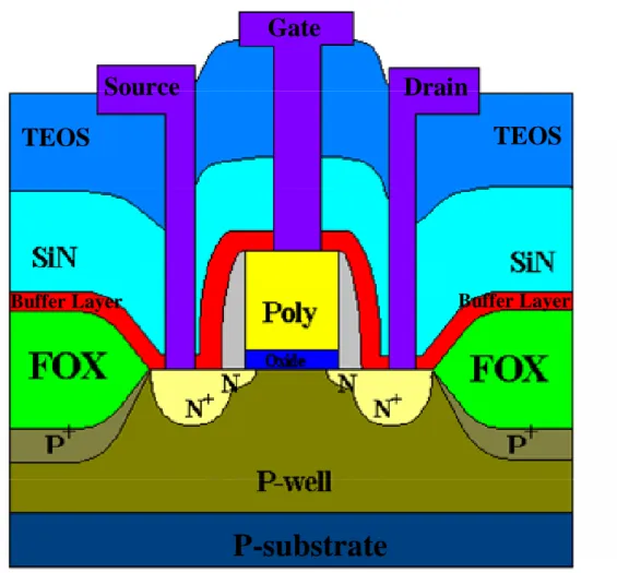
Afterwards, some samples were capped with a TEOS or a poly-Si to serve as the buffer layer. The thickness of the buffer layer is 10 nm. Then a SiN capping layer (contact-etch-stop-layer, CESL) of 300nm was deposited on some wafers both with or without the buffer layer. The SiN deposition was performed at 780 ℃ with SiH2Cl2 and NH3 as the reaction precursors using low-pressure chemical vapor deposition (LPCVD) system. After the SiN capping, a 300nm TEOS passivation layer was deposited by an LPCVD system.
To simulate the effect of deposition temperature during the SiN deposition, the control devices (i.e., without SiN capping) received a placebo treatment (i.e., the same temperature and treatment time as that used in the SiN deposition) in N2 ambient. After contact hole etching, normal metallization was carried out for all samples. The final step was a forming gas anneal performed at 400°C for 30 min to mend dangling bonds and
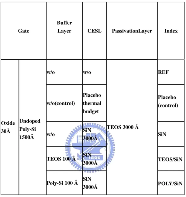
reduce interface state density in the gate oxide/Si interface. Cross-sectional view of the fabricated device was shown in Fig. 2.1.The five split conditions stated above are summarized in Table 2.1.
2.2 Electrical Measurement Setup
by an HP4156A precision semiconductor parameter analyzer and an HP4284 LCR meter, respectively. Temperature-regulated hot chucks were used to maintain the measurement temperature at 25°C.
2.3 Charge Pumping Measurement
2.3.1 Basic Theory
The charge pumping principle for MOSFETs has been applied to characterize the fast interface traps in MOSFETs. The original charge pumping method was introduced by Brugler and Jespers [32], and the technique was then developed by Heremans [33]. This technique is based on a recombination process at the Si/SiO2 interface involving the surface traps. It consists of applying a constant reverse bias at the source and drain, while sweeping the base level of the gate pulse train from a low accumulation level to a high inversion level. The frequency and the rise/fall time are kept constant. When the base level is lower than the flat-band voltage while the top level of the pulse is higher than the threshold voltage, the maximum charge pumping current occurs. This means that a net amount of charge is transferred from the source and drain to the substrate via the fast interface traps each time the device is pulsed from inversion toward accumulation. The charge pumping current is caused by the repetitive recombination at interface traps. As a result, the recombination current measured from the bottom
(substrate) is the so-called charge pumping (CP) current [34]. The CP current can be given by:
ICP = q · f · W · L · Nit. (2.1)
According to this equation, the current is directly proportional to the interface trap density in the channel, the frequency, and the area of the device. However, when the top level of the pulse is lower than the flat-band voltage or the base level is higher than the threshold voltage, the fast interface traps are permanently filled with holes in accumulation or the electrons in inversion in NMOSFETs. As a result, there is no recombination current and no charge pumping current can be detected.
2.3.2 Basic Measurement Setup
The basic setup of charge pumping measurement is shown in Fig. 2.2. In this thesis, “fixed amplitude sweep” is used to calculate interface trap density, and “fixed base sweep” is used to analyze the lateral distribution of interface trap, respectively. The source and drain are biased at 50mV. The substrate electrodes of tested devices are grounded. A 1MHz (the frequency can be modulated for different devices) square pulse waveform provided by HP8110A with fixed amplitude is applied to the NMOS gate. The base voltage is varied to let surface condition switch from inversion to accumulation, while keeping the pulse amplitude at 1.5V. In our measurement setup, Vbase is varied from -2V to -0.2V in step of 0.05V. The parameter analyzer HP4156A is
used to measure the charge pumping current (ICP).
2.4 Hot Carrier Reliability Measurement Setup
In our reliability measurement, the device was stressed with the drain voltage at a highly positive voltage, and the gate terminal biased at the voltage where maximum Isub occurs to accelerate the degradation. So we must first measure the Isub-VG with a fixed drain bias to find VG@Isubmax, before stressing the device. To monitor the degradation caused by the hot electrons, the ID-VG characteristics at VDS = 0.05 V (linear region) and charge pumping current were measured before and after the stress. The degradations in terms of threshold voltage shift (∆Vth), interface trap density degradation (∆Nit), and transconductance degradation (∆Gm), were recorded in the accelerated stress test.
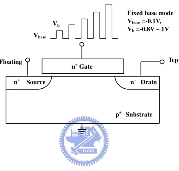
2.5 Extraction Procedure of Lateral Distribution of
Nit
The lateral distribution of interface state after hot carrier stress of all splits was also discussed in this work. This method builds on [35] and the measurement setup is shown in Fig. 2.3. The experimental procedures are described below.
(1) Measure the Icp-Vh curve on a virgin MOSFET from the drain junction (with the source junction floating), and from which the relationship between Vh and Vth(x) near the junction of interest is established [36].
(3) The hot-carrier-induced interface state distribution, Nit(x), is obtained from the difference of the Icp-Vh curves before and after the stress.
Chapter 3
Experimental Results and Discussion
3.1 Electrical Characteristics of Locally Strained
NMOSFETs with Buffer Layer
3.1.1 Fundamental Electrical Characteristics
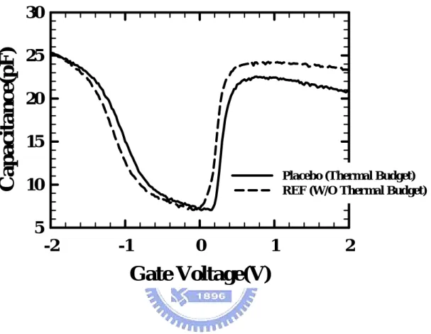
First of all, our goal is to investigate the effect of thermal budget associated with the SiN deposition. So, for the placebo split, we deliberately added an additional thermal treatment step in N2 with an identical temperature and treatment time as those used in the SiN deposition (i.e., at 780℃ ambient for 3 hours) before the TEOS passivation layer deposition. Samples which were skipped both the SiN deposition and the thermal N2 annealing steps were also fabricated for comparison, denoted as the REF (reference) split. Fig.3.1 shows the effect of such placebo thermal treatment on the capacitance-voltage(C-V) characteristics of devices without SiN capping.In this figure, the device with the additional thermal budget (placebo split) shows apparent poly-depletion effect. We believe this is caused by the temperature-dependent solid solubility of dopants in poly gates [37], as shown in Fig. 3.2. In other words, the original solid solubility (approaching the equilibrium value at 900℃, which is caused by the rapid thermal anneal (RTA) step) is lowered by the furnace SiN deposition step
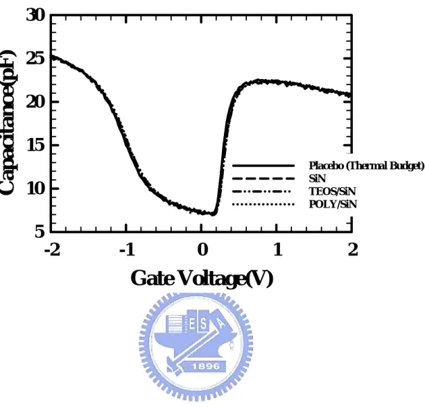
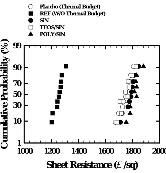
due to the additional thermal budget. The placebo split shows larger threshold voltage due to the reduction of fixed charge in gate oxide. The C-V characteristics of MOSFETS are also important in verifying the oxide quality and the equivalent oxide thickness (EOT). Fig. 3.3 exhibits C-V characteristics of NMOSFETs for all splits (i.e. placebo (thermal budget), SiN, TEOS/SiN, POLY/SiN). The curves of four splits are basically identical. It gives an equal ground to compare the performance of all splits. So the split with placebo thermal budget (i.e., the placebo split) serves the role of the control split, and will also be called the control split interchangeably. Fig. 3.4 shows cumulative probability distributions of the sheet resistance of the poly gate for all splits. The REF (i.e., W/O thermal budget) split has lower sheet resistance values, while the other four splits exhibit almost same distribution of sheet resistance. This demonstrates that the additional thermal treatment step used in the SiN deposition indeed results in worse poly-depletion effect.
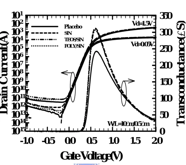
The Id-Vg characteristic of the split conditions are shown in Fig. 3.5. From the figure, there is no obvious difference in the transconductance (Gm) among all samples except the placebo split, clearly revealing the enhancement of transconductance by the strained technology. The off-state leakage current and the subthreshold slope show no distinguishable difference in Fig. 3.5, indicating that the devices with strained channel do not show major influence on the fundamental properties. Fig. 3.6 depicts the
subthreshold swing for all splits, and the results indicate that the values are confined in a narrow range between 74~75 mV/decade. The output characteristics of all splits are shown in Fig. 3.7. It is seen that the insertion of the buffer layer prior to SiN deposition (i.e., TEOS/SiN, POLY/SiN) does not degrade the current enhancement. Consistent with previous literature report [38], the NMOS drive current can be enhanced by a thicker SiN etch-stop layer which is tensile in nature.
Fig. 3.8 shows the percentage increase of the transconductance among different splits relative to the placebo devices (i.e., w/o SiN capping). The transconductance enhancement reaches about 29% and 33% at a channel length of 0.5µm and 0.4µm, respectively. We can see that when the channel length decreases, the strain effect enhances. In other words, the strain is distributed locally inside the channel and concentrated near the source and drain. As a result, the transconductance enhancement becomes more prominent with decreasing channel length. This is explained by the splitting of the degeneracy at the conduction band edges under uniaxial strain [24] as mentioned above. Fig. 3.9 exhibits the percentage increase of the saturation current for the split samples relative to the placebo devices (i.e., w/o SiN capping). From Fig. 3.9, it can be seen that similar trend to that shown in Fig. 3.8 is observed.
Fig. 3.10 shows the results of charge pumping measurement for some splits (i.e., placebo (thermal budget), REF, and SiN). First, we focus on the impact of thermal
budget associated with the SiN deposition. From the figure, we find that a large amount of interface states is generated during SiN capping process as compared with the samples without the capping layer, implying that the channel strain indeed causes the increase of interface states at the Si/SiO2 interface. Nevertheless, it is well known that hydrogen species can effectively passivate the dangling bonds at the Si/SiO2 interface. For the LPCVD system used for SiN deposition in this study, SiH2Cl2 and NH3 were employed as the reaction precursors, so the reaction chamber would be filled with hydrogen species during the deposition process. The hydrogen species would in turn passivate the interface trap states at the Si/SiO2 interface. Although this factor should not be ignored, in this figure such effect obviously is masked by the channel strain. In other words, the number of interface states passivated by the hydrogen species is much less than that generated by the channel strain.
On the other hand, the figure also proves that the annealing performed in N2 tends to reduce the interface states density, indicating this factor (thermal budget of the deposition) alone is beneficial for improving the interface properties. From Fig. 3.10, impacts of the three factors, namely, channel, incorporated hydrogen species, and the thermal budget, on interface state density are identified.
Comparisons of charge pumping current between the strain and placebo samples are shown in Fig. 3.11. The placebo sample exhibits the lowest charge pumping current
among all splits, while the device with TEOS buffer layer exhibits the highest. The curve of the device with POLY/SiN is slightly higher than that with SiN, but less than that with TEOS buffer layer. The results indicate that the TEOS buffer layer can effectively block the diffusion of hydrogen into the channel region, while such barrier effect seems to be reduced for the POLY buffer layer. It has been pointed out previously that the poly-silicon is a diffusion barrier of the hydrogen [39]. But it should be noted that, the precursor gas (SiH4) for deposition is also H-containing. Before the SiN deposition, the abundant hydrogen species may have spread to the Si/SiO2 interface to passivate the interface states. In summary, TEOS buffer layer has been shown to be more effective in blocking the hydrogen diffusion into the Si/SiO2 interface.
3.1.2 Short Channel effect
Threshold voltage (Vth) roll-off characteristics of the placebo (thermal budget) and REF splits are shown in Fig. 3.12. The results are obtained at VDS = 0.05 V. From the figure, both splits depict reverse-short-channel-effect (RSCE). This can probably be explained by boron segregation at the implant-damaged regions located near the edge of the channel [40]. Devices with additional thermal budget show improved reverse-short-channel-effect [40]. It might be related to the redistribution of dopants that effectively reduces the boron segregation effect, explaining the suppression of the RSCE shown in Fig. 3.12.
In Fig. 3.13, it is worth noting that the placebo samples depict the reverse-short-channel-effect (RSCE). However, this phenomenon is not observed on three SiN-capped splits (SiN, TEOS/SiN, POLY/SiN). Instead, theses three splits exhibit similar and significant threshold voltage roll-off trend. It is believed that the bandgap narrowing effect is the culprit to accelerate the Vth roll-off in the strained channel device [28, 41]. The strain stress may also result in the channel dopants redistribution [42, 43]. In brief, the channel strain associated with the SiN capping devices (SiN, TEOS/SiN, POLY/SiN) would lead to aggravated Vth roll-off.
Drain induced barrier lowing (DIBL) is another pointer in evaluating the short channel effects. We use the interpolation method to calculate DIBL effect for all splits. The results are shown in Fig. 3.14. It is clearly seen that there is no distinguishable difference among all splits. It appears that devices with SiN capping and buffer layers will not complicate the DIBL effect of the samples.
3.2 Hot Carrier Degradation of Locally Strained
NMOSFETs with Buffer Layer
A hot carrier with sufficient energy can create more charge carriers through impact ionization. For NMOSFET devices, holes generated by impact ionization are collected by the substrate. Fig. 3.15 shows the substrate current (Isub) versus gate voltage for all splits of devices at VD of 4.6 V. It can be seen that the three strained-channel splits
exhibit almost identical maximum substrate current which are much higher than that of placebo sample. This result shows clearly that the channel strain plays an important part in affecting the generation of channel hot electrons and the associated impact ionization process. Bandgap narrowing and mobility enhancement, both due to channel strain, are mainly responsible for enhancing the ionization rate [44]. So the SiN-capped devices show larger substrate current than the placebo samples.
Hot-carrier effects and the induced degradation were investigated to study the impact of the SiN capping and buffer layers.As discussed above, it is expected that the split with SiN capping (i.e. SiN) would show aggravated hot carrier degradation. Fig. 3.16 and Fig. 3.17 show threshold voltage shift and increased interface state density, respectively, as a function of stress timefor all splits that received hot-electron stressing at VDS = 4.6 V and VGS at maximum substrate current. All devices are with channel width/length = 10µm/0.5µm. As expected, the split with SiN capping shows the worst hot carrier degradation, and the use of buffer layer apparently improves hot carrier degradation. We assume that the bandgap narrowing effect and the increased carrier mobility in the strained channel devices [44, 45] are the two primary culprits for the aggravated hot carrier degradations. These two factors may increase the substrate current in the device, as evidenced in Fig. 3.15, and lead to higher degradation.
degradation process. Since the hot carriers tend to break the Si-H bonds during the process, the higher the amount of the Si-H density, the severer the degradation. The TEOS buffer layer can block the diffusion of hydrogen species into the channel region, less broken Si-H bonds and thus less interface states are generated during the stressing as compared with the SiN-capped devices. As a consequence, better reliability is achieved, as evidenced in Fig. 3.16 and Fig. 3.17. For the devices with POLY buffer layer, less improvement is achieved due to higher amount of Si-H bonds, as stated above. Fig. 3.18 illustrates the 10-year reliability projections for the four splits. Lifetime is defined as 40mV of ΔVth. The observed trend is the same as that shown in Fig. 3.16. Strained devices show poor hot carrier reliability than placebo device, although the use of buffer layer can alleviate hot carrier degradation.
Typical results of hot-electron stressing for the four splits of samples are shown in Fig. 3.19 and Fig. 3.20. Channel width and length of the test devices are 10μm and 0.5 μm, respectively. The devices are stressed at VDS = 4.9 V and VGS at maximum substrate current. The ID-VG characteristics at VDS = 0.05 V are measured before and after the stress to evaluate the degradation caused by the hot electrons. As shown in Fig. 3.19 and Fig. 3.20, the degradation is the worst in the SiN-capped sample without buffer layer among the four splits. The aggravation is alleviated in the devices with buffer layer (i.e. TEOS/SiN, POLY/SiN), though the resultant degradation is still worse than
that of the placebo counterpart.
3.3 Analysis of the Lateral Distribution of Interface
Trap Density
The measurement methods presented in Section 2.5 was used to extract lateral distribution of interface trap state. It should be noted that the local Vth and Vfb, across the channel of MOSFET, are not uniform due to the lateral doping variation, as shown in Fig. 3.21. In order to detect the interface state, the voltage pulses applied during measurement must undergo alternating accumulation and inversion cycles. Therefore, there should be no Icp when the high-level voltage (Vh) is lower than the minimum Vth under the gate. Only after Vh starts to exceed the local Vth in the channel will Icp begin to grow. Before Vh reaches the maximum local Vh in the channel, only interface states residing near the drain side will contribute to Icp, as the needed electrons cannot yet flow to the drain side from the source.
We choose the placebo split as an example. If we assume that the interface state density is spatially uniform along the channel, which can be written as
ICP = q · f · W · L · Nit. (3-1)
where f is the gate pulse frequency, W is the channel width, and L is the channel length. Since Vth is not uniformly distributed, when Vh reaches the maximum local Vth in the channel, only interface state residing near the drain side (i.e., the shadow region
in Fig. 3.21) will contribute to Icp. In Fig. 3.22, the corresponding Icp(Vh) comes from the interface state distributed in the region between the gate edge and the position where its local Vth equals Vh, i.e.,
( )
cp h it
I V =q f N W x (3-2) where x represents the distance from the gate edge to the position where Vth (x) = Vh. Comparing (3-1) and (3-2), we can derive
( )
max , cp h cp I V LI x= (3-3)Fig.3.23 shows the local Vth versus distance x of the placebo sample. The local Vth decreases sharply as x is smaller than 0.09 µm. We can therefore presume that the drain junction is near x = 0.09 µm.
After subjecting to 100 second of hot carrier stress (VG@Isubmax and VDS = 4.9 V), the incremental charge pumping current (∆Icp), as shown in Fig. 3.24, at a given Vh is
proportional to the number of generated interface traps from the gate edge to the point x. ∆Icp can be written as
( )
0 x cp it I q f W N x dx ∆ =∫
(3-4) Therefore, the Nit(x) generated by the hot carrier stress can be expressed as follows:( )
1 1 cp cp h it h d I d I dV N x dx q f W dV dx q f W ∆ ∆ = = (3-5)The relationship of dVh
dx versus x can be derived from Vh versus x, so the lateral
distribution, Nit (x), could be obtained from the procedure mentioned above.
By the same procedure, the derived profiles of the interface states for all splits of devices could be extracted by Eq.(3-5), and the result are shown in Fig. 3.25. From this figure we can directly probe the position-dependent damage characteristics by calculating the amount of interface states generated by the hot-carrier stress at different regions. We can see that the major damage region is confined within 0.1 µm near the
drain edge in all splits. This is reasonable since the hot-carrier effect is known to be localized in nature. It is obviously seen that the interface state generation sharply increases in SiN-capped sample (i.e. SiN, TEOS/SiN, POLY/SiN) near the drain region, but the buffer layer samples show smaller degradation than the SiN-capping split without buffer layer. These results are consistent with those mentioned above in Section 3.2. In short, channel strain is responsible for the aggravated hot carrier degradations observed in SiN-capped samples. However, the devices with buffer layer show alleviated hot carrier degradation and improved device reliability.
Chapter 4
Summary and Conclusion
4.1 Summary and Conclusion
In this thesis, the effects of LPCVD SiN layer and the associated deposition process on the device characteristics and hot-electron degradation are investigated. A novel scheme involving the insertion of a buffer layer between the SiN and the gate for improving the device reliability was proposed and demonstrated. Several important phenomena are observed and summarized as follows:
(1) The buffer layer before SiN deposition would not degrade the device performance. For example, the enhancement ratio of transconductance in the device with the buffer layer is found to be around to 33% at a channel length of 0.4μm, which is essentially identical to the enhancement ratio observed in the SiN-capped device.
(2) The thermal budget associated with the deposition of the SiN capping layer could reduce the interface states and alleviate the reverse short-channel effect, although the poly-depletion effect becomes worse. The bandgap narrowing effect due to the channel strain may result in further lowering in Vth as the channel length is shortened.
to the use of the H-containing precursor (e.g. SiH4) in the deposition step.
(4) Hot-electron degradation is adversely affected when the SiN is deposited over the gate as compared with the placebo samples. When a buffer layer is capped prior to the SiN deposition, although still worse than the placebo ones, significant improvement over that without the buffer could be obtained. From the measurement of the distribution of interface trap density, enhance edge effects caused by the hot carrier stress are resolved.
In this work, we found that hydrogen species is the primary culprit for aggravated reliabilities in strained devices. The insertion of a buffer layer serves to alleviate the device hot-carrier degradations. Optimization of SiN deposition process and/or use of the new buffer layer (e.g., high-k film) are thus essential for the implementation of the uniaxial strain in NMOS devices.
Reference:
[1] S.H. Olsen, K.S.K. Kwa, L.S. Driscoll, S. Chattopadhyay and A.G. O’Neill, “Design, fabrication and characterisation of strained Si/SiGe MOS transistors”, IEE
Proc.-Circuits Devices Syst., Vol. 151, No. 5, October 2004.
[2] J. L. Hoyt, H. M. Nayfeh, S. Eguchi, I. Aberg, G. Xia, T. Drake, E. A. Fitzgerald, D. A. Antoniadis, “Strained silicon MOSFET technology”, in IEDM Tech. Dig., pp. 23-26, 2002.
[3] T. Ghani, M. Armstrong, C. Auth, M. Bost, P. Charvat, G. Glass, T. Hoffmann, K. Johnson, C. Kenyon, J. Klaus, B. McIntyre, K. Mistry, A. Murthy, J. Sandford, M. Silberstein, S. Sivakumar, P. Smith, K. Zawadzki, S. Thompson, and M. Bohr, “A 90nm high volume manufacturing logic technology featuring novel 45nm gate length strained silicon CMOS transistors”, in IEDM Tech. Dig., pp. 978-980, 2003. [4] S. Pidin, T. Mori, K. Inoue, S. Fukuta, N. Itoh, E. Mutoh, K. Ohkoshi, R. Nakamura,
K. Kobayashi, K. Kawamura, T. Saiki, S. Fukuyama, S. Satoh, M. Kase, and K. Hashimoto, “A novel strain enhanced CMOS architecture using selectively deposited high tensile and high compressive silicon nitride films”, in IEDM Tech.
Dig., pp. 213-216, 2004.
[5] C. Y. Lu, H. C. Lin, Y. F. Chang, and T. Y. Huang, “Device characteristics and aggravated negative bias temperature instability in PMOSFETs with uniaxial compressive strain”, int. Conference on Solid State Devices and Materials, pp. 874-875, 2005.
[6] E. Li, E. Rosenbaum, J. Tao, and P. Fang, “projecting lifetime of deep submicron MOSFETs”, IEEE Trans. on Electron Devices, vol. 48, pp. 671-678, April 2001.
Katsumata, and H. Iwai, “A study of hot-carrier degradation in n- and p-MOSFETs with ultra-thin gate oxides in the direct-tunneling regime”, in IEDM Tech. Dig., pp. 453-456, 1997.
[8] A. Schwerin, W. Hansch, and W. Weber, “The relationship between oxide charge and device degradation: A comparative study of n- and p- channel
MOSFET's”, IEEE Trans. on Electron Devices, vol. ED-34, pp. 2493-2500, December 1987.
[9] P. Heremans, R. Bellens, G. Groeseneken, and H. Maes, “Consistent model for the hot-carrier degradation in n-channel and p-channel MOSFETs”, IEEE Trans. on
Electron Devices, vol. 35, pp. 2194-2209, December 1988.
[10] C. Y. Lu, “A Study of Drive Current Enhancement Methods and Related Reliability Issues for MOSFETs”, A Dissertation in Department of Electronics Engineering &
Instisute of Electronics in NCTU, pp. 122-148, July 2006
[11] S. Takagi, T. Mizuno, T.Tezuka, N. Sugiyama, T. Numata, K.Usuda, Y. Moriyama, S. Nakaharai, J. Koga, A. Tanabe, N. Hirashita, and T. Maeda, “Channel structure
design, fabrication and carrier transport properties of strained-Si/SiGe-on-insulator (strained-SOI) MOSFETs”, in IEDM Tech. Dig., pp.57-60, December 2003.
[12] S. E. Thompson, M. Armstrong, C. Auth, S. Cea, R, Chau, G. Glass, T, Hoffman, J. Klaus, Z. Ma, B. Mcintyre, A. Murthy, B. Obradovic, L. Shifren, S. Sivakumar, S. Tyagi, T. Ghani, K. Mistry, M. Bohr, and Y. El-Mansy, “A logic nanotechnology featuring strained-silicon”, IEEE Electron Device Lett., vol. 25, pp.191-193, April 2004.
[13] W. Zhao, J.He, R. E. Belford, L. Wernersson, and A. Seabaugh, “Partially depleted SOI MOSFETs under uniaxial tensile strain”, IEEE Trans. Electron
and D. A. Antoniadis, “Straind silicon MOSFET technology”, in IEDM Tech. Dig., pp.23-26,December 2002.
[15] A. Shimizu, K. Hachimine, N. Ohki, H. Ohta, M. Koguchi, Y. Nonaka, H. Sato, and F. Ootsuka, “Local mechanical-stress control (LMC): A new technique for CMOS-performance enhancement”, IEDM Tech. Dig., pp. 433-436, December 2001.
[16] G. Scott, J. Lutze, M. Rubin, F. Nouri, and M. Manley, “NMOS Drive current reduction caused by transistor layout and trench isolation induced stress”, IEDM
Tech. Dig., pp.827-830, December 1999.
[17] T. Ghani, M. Armstrong, C. Auth, M. Bost, P. Charvat, G. Glass, T. Hoffmann, K. Johnson, C. Kenyon, J. Klaus, B. McIntyre, K. Mistry, A. Murthy, J. Sandford, M. Silberstein, S. Sivakumar, P. Smith, K. Zawadzki, S. Thompson, and M. Bohr, “A 90nm high volume manufacturing logic technology featuring novel 45nm gate length strained silicon CMOS transistors”, IEDM Tech. Dig., pp.978-980, December 2003.
[18] A. Steegen, M. Stucchi, A. Lauwers, and K. Maex, “Silicide induced pattern density and orientation dependent transconductance in MOS transistors”, IEDM
Tech. Dig., pp.497-500, December 1999.
[19] S. Maikap, M. H. Liao, F. Yuan, M. H. Lee, C. Huang, S. T. Chang, and C. W. Liu, ”Package-strain-enhanced device and circuit performance”, IEDM Tech. Dig., pp.233-236, December 2004.
[20] C. Hu, “Device challenges and opportunities”, in Symp. VLSI Tech. Dig., pp.4-5, 2004
[21] S. Ito, H. Namba, K. Yamaguchi, T. Hirata, K. Ando, S. Koyama, S. Kuroki,N.Ikezawa, T. Suzuki, T. Saitoh, and T. Horiuchi, “Mechanical stress effect
Tech. Dig., pp.247-250, December 2000.
[22] C. Zhi-Yuan, M. T. Currie, C. W. Leitz, G. Taraschi, E. A. Fitzgerald, J. L. Hoyt, and D. A. Antoniadis, “Electron mobility nhancement in strained-Si n-MOSFET fabricated on SiGe-on-insulator (SGOI) substrates”, IEEE Electron Device Lett., vol.22, pp.321-323, July 2001.
[23] S. E. Thompson, G. Sun, K. Wu, J. Kim, and T. Nishida, “Key differences for process-induced uniaxial vs. substrate-induced biaxial stressed Si and Ge channel MOSFETs”, IEDM Tech. Dig., pp.221-224, December 2004.
[24] B. M. Haugerud, L. A. Bosworth, and R. E. Belford, “Mechanically induced strain enhancement of metal--oxide--semiconductor field effect transistors”, J. Appl.
phys., Vol.94, pp.4102-4107, 2003
[25] M.D.Giles, M.Armstrong, C.Auth, S.M.Cea, T.Ghani, T.Hoffmann, R.Kotlyar, P.Matagne, K.Mistry, R.Nagisetty, B.Obradovic, R.Shaheed, L.Shifren, M.Stettler, S.Tyagi, X.Wang, C.Weber, K.Zawadzki, “Understanding stress enhanced performance in Intel 90nm CMOS technology”, VLSI Symp. Tech. Dig., pp.118-119, 2004
[26] C. W. Leitz, M. T. Currie, M. L. Lee, Z. -Y. Cheng, D. A. Antoniadis and E. A. Fitzgerald, “Hole mobility enhancements and alloy scattering-limited mobility in tensile strained Si/SiGe surface channel metal–oxide–semiconductor field-effect transistors”, J. Appl. phys., Vol.92, pp.3745-3751, 2002
[27] M. V. Fischetti, Z. Ren , P. M. Solomon, M. Yang, and K. Rim, “Six-band k·p calculation of the hole mobility in silicon inversion layers: Dependence on surface orientation, strain, and silicon thickness”, J. Appl. phys., Vol.94, pp.1079-1095, 2003
Electron Device Lett., Vol. 24, pp.568-570, September 2003.
[29] E. Li, E. Rosenbaum, J. Tao, and P. Fang, “Projecting lifetime of deep Submicron MOSFETs”, IEEE Trans. on Electron Devices, vol. 48,pp. 671-678, April 2001. [30] H. S. Momose, S. Nakamura, T. Ohguro, T.Yoshitomi, E. Morifuji, T. Morimoto, Y.
Katsumata, and H. Iwai, “A study of hot-carrier degradation in n- and p-MOSFETs with ultra-thin gate oxides in the direct-tunneling regime”, in IEDM Tech. Dig., pp.453-456, 1997.
[31] H. Hazama, M. Iwase, and S. Takagi, “Hot-carrier reliability in deep submicrometer MOSFETs”, in IEDM Tech. Dig., pp.569-572, 1990.
[32] J.S. Brugler, and P.G.A. Jespers, “Charge Pumping in MOS Devices”, IEEE Trans.
on Electron Devices, vol. 16, pp. 297-302, March 1969.
[33] P. Heremans, J. Witters, G. Groeseneken,and H. E. Maes, “Analysis of the charge pumping technique and its application for the evaluation of the MOSFET Degradation”, IEEE Tran. Electron Devices, Vol. 36, No. 7, pp. 1318-1335, 1989. [34] G. Groeseneken, H. E. Maes, N. Beltran, and R. F. De Kecrsmaecker, “A reliable
approach to charge-pumping measurements in MOS transistors”, IEEE Trans.
Electron Devices, Vol. ED-31, pp. 42-53, 1984.
[35] C. Chen, and T. P. Ma, “Direct lateral profiling of hot-carrier-induced oxide charge and interface traps in thin gate MOSFET’s”, IEEE Electron Devices, vol.45, pp.512-520, February 1998.
[36] M. Tsuchiaki, H. Hara, T. Morimoto, and H. Iwai, “A new charge pumping method for determining the spatial distribution of hot-carrier induced fixed charge in p-MOSFET’s”, IEEE Trans. Electron Devices, vol. 40, pp. 1768–1778, October 1993.
Murthy, J. Sandford, R. Shaheed, K. Zawadzki, K. Zhang, S. Thompson, M. Bohr, “Delaying forever: Uniaxial strained silicon transistors in a 90nm CMOS technology”, VLSI Symp. Tech. Dig., pp. 50-51, June 2004.
[39] W. B. Jackson, N. WI. Johnson, C. C. Tsai, L-W. Wu, A. Chiang, and D. Smith, “Hydrogen diffusion in polycrystalline silicon thin films”, American Institute of
Physics, pp. 1670-1672, October 1992.
[40] H. I. Hanafi, W. P. Noble, R. S. Bass, K. Varahramyan, Y. Lii, and A. J. Dally, “A model for anomalous short-channel behavior in submicron MOSFETs”, IEEE
Electron Device Lett., vol. 14, pp. 575-577, Decmber 1993.
[41] J.-S. Lim, S.E. Thompson, J.G. Fossum, “Comparison of threshold voltage shifts for uniaxial and biaxial tensile-stressed n-MOSFETs”, IEEE Electron Device
Letters, vol. 25, pp. 731-733, November 2004.
[42] S. T. Dunham, M. Diebel, C. Ahn, and C. L. Shih, “Calculations of effect of anisotropic stress/strain on dopant diffusion in silicon under equilibrium and nonequilibrium conditions”, American Vacuum Society, pp.456-461, January 2006. [43] L. Lin, T. Kirichenko, B. R. Sahu, G. S. Hwang, and S. K. Banerjee, “Theoretical
study of B diffusion with charged defects in strained Si”, The American Physical Society, 2005
[44] M. F. Lu, S. Chiang, A. Liu, S. H. Lu, M. S. Yeh, J. R. Hwang, T.H. Tang, W.T. Shiau, M. C. Chen and T. Wang, “Hot carrier degradation in novel strained-Si nMOSFETs”, in Proc. Int. Reliability Physics Symp., pp. 18-22, 2004.
[45] N. Sano, M. Tomizawa, and A. Yoshii, “Temperature dependence of hot carrier effects in short-channel Si-MOSFETs”, IEEE Trans. on Electron Devices, vol. 42, pp. 2211-2216. December 1995.
Gate
Buffer
Layer CESL PassivationLayer Index
w/o w/o REF
w/o(control) Placebo thermal budget Placebo (control) w/o SiN 3000Å SiN TEOS 100 Å SiN 3000Å TEOS/SiN Oxide 30Å Undoped Poly-Si 1500Å Poly-Si 100 Å SiN 3000Å TEOS 3000 Å POLY/SiN
Fig. 1.1 Gate length scaling as a function of the year of introduction for technology node [1].
CMOS Performance Impact
Direction of
Strain Change*
NMOS PMOS
X
Improve Degrade
Y
Improve
Improve
Z Degrade
Improve
* Strain change = Increased tensile or decreased compressive strain
Drain
Gate
Ex
Ey
Ez
Source
Gate
Silicide
Process-induced Strain
Fig. 1.3 Splitting of light hole band and heavy hole band with biaxial and uniaxial strains in low electric field (solid line) and high electric field (dash line) [22].
LH
LH HH
HH
ΔELH-EHH
ΔELH-EHH
Gate
P-substrate
Source
Drain
TEOS
TEOS
Buffer Layer Buffer LayerGate
P-substrate
Source
Drain
TEOS
TEOS
Buffer Layer Buffer LayerFig. 2.3 Measurement setup of single-junction charge pumping measurement.
Icp
Floating
n
+Drain
n
+Source
n
+Gate
Fixed base mode
V
base=-0.1V,
V
h=-0.8V ~ 1V
V
baseV
hFig. 3.1 Capacitance-Voltage(C-V) characteristics of NMOSFETs processed with different thermal budgets. Channel width/channel length = 50μm/50μm.
Gate Voltage(V)
-2
-1
0
1
2
Capacitance(pF)
5
10
15
20
25
30
Placebo (Thermal Budget) REF (W/O Thermal Budget)
Fig. 3.3 Capacitance-Voltage(C-V) characteristics of different splits of NMOSFETs. Channel width/channel length = 50μm/50μm.
Gate Voltage(V)
-2
-1
0
1
2
Capacitance(pF)
5
10
15
20
25
30
Placebo (Thermal Budget) SiN
TEOS/SiN POLY/SiN
Fig. 3.4 Cumulative probability distribution of poly-gate sheet resistance for all splits of samples. The film thickness is 150nm. Doping was done by As-ion implantation at a dose of 3x1015 cm-2 and an energy of 10KeV. All samples received an RTA at 900℃ for 30sec. Note that the REF split skips the thermal treatment associated with the SiN deposition.
Sheet Resistance (
Ω/sq)
1000
1200
1400
1600
1800
2000
Cumulative Probability (%)
1
10
30
50
70
90
99
Placebo (Thermal Budget) REF (W/O Thermal Budget) SiN
TEOS/SiN POLY/SiN
Fig. 3.5 Subthreshold and transconductance characteristics of different splits of NMOSFETs characterized at 25℃. Channel width/channel length = 10μm/0.5μm.
Gate Voltage(V)
-1.0
-0.5
0.0
0.5
1.0
1.5
2.0
Drain Current(A)
10
-15
10
-14
10
-13
10
-12
10
-11
10
-10
10
-9
10
-8
10
-7
10
-6
10
-5
10
-4
10
-3
10
-2
10
-1
Transconductance
(µ
S
)
0
50
100
150
200
250
300
350
Control SiN TEOS/SiN POLY/SiNW/L=10
µm/0.5µm
Vd=1.5V
Vd=0.05V
PlaceboPla
ceb
o
Subthreshold Swing(mV/dec)
70
72
74
76
78
80
SiN
TE
OS
/Si
N
PO
LY
/Si
N
Fig. 3.6 Subthreshold swing for different splits of NMOSFETs. Channel width/channel length = 10μm/0.5μm.
W/L=10
µm/0.5µm
Drain Voltage(V)
0.0
0.5
1.0
1.5
2.0
Drain Current(mA)
0
1
2
3
4
5
6
Placebo SiN TEOS/SiN POLY/SiN V G-Vth=0.4~2V, Step=0.8VFig. 3.7 Output characteristics of NMOSFETs for different splits, measured at 25℃. Channel width/channel length = 10μm/0.5μm.
Fig. 3.8 Transconductance enhancement for different splits as a function of channel length, measured at 25°C.
Gate Length(
µm)
1
10
∆
G
m,max
/G
m,ma
x,co
ntro
l(%)
0
10
20
30
40
SiN
TEOS/SiN
POLY/SiN
Fig. 3.9 Drain current enhancement for different splits as a function of channel length, measured at 25°C. The saturation current was measured at VG-Vth = 2V and VDS = 2V.
![Fig. 1.1 Gate length scaling as a function of the year of introduction for technology node [1]](https://thumb-ap.123doks.com/thumbv2/9libinfo/8019852.160773/51.892.155.671.257.717/fig-gate-length-scaling-function-year-introduction-technology.webp)
![Fig. 1.3 Splitting of light hole band and heavy hole band with biaxial and uniaxial strains in low electric field (solid line) and high electric field (dash line) [22]](https://thumb-ap.123doks.com/thumbv2/9libinfo/8019852.160773/53.892.160.748.314.751/splitting-light-biaxial-uniaxial-strains-electric-field-electric.webp)
![Fig. 3.2 Solid solubility of various elements in Si as a function of temperature [37]](https://thumb-ap.123doks.com/thumbv2/9libinfo/8019852.160773/58.892.153.648.106.752/fig-solid-solubility-various-elements-si-function-temperature.webp)