784 IEEE ELECTRON DEVICE LETTERS, VOL. 29, NO. 7, JULY 2008
Temperature-Dependent Capacitance Characteristics
of RF LDMOS Transistors With Different
Layout Structures
Hsin-Hui Hu, Kun-Ming Chen, Guo-Wei Huang, Member, IEEE, Ming-Yi Chen,
Eric Cheng, Yu-Chi Yang, and Chun-Yen Chang, Fellow, IEEE
Abstract—In this letter, the capacitance characteristics of RF
LDMOS transistors with different temperatures and layout struc-tures were studied. In a conventional fishbone structure, the peaks in capacitances decrease with increasing temperature. For the ring structure, two peaks in a capacitance–voltage curve have been observed at high drain voltages due to the additional corner effect. In addition, peaks in gate-to-source/body capacitance decrease and peaks in gate-to-drain capacitance increase with increasing temperature at high drain voltages. By analyzing the effects of temperature on threshold voltage, quasi-saturation current, and drift depletion capacitance, the variations of capacitances with temperature were investigated.
Index Terms—Capacitance, drift region, laterally diffused MOS
(LDMOS), layout structure, nonuniform doping, temperature.
I. INTRODUCTION
R
F POWER amplifiers are key components in base stations for personal communication systems [1]. Due to its ad-vantages in performance, cost, reliability, and power capability, laterally diffused MOS (LDMOS) transistor technology has played a predominant role in the power amplifier applications [2]. Because the device capacitances influence the input, output, and feedback capacitances, which are important in the dynamic operation, and have large impact on device high-frequency performance, the capacitance characterization and modeling of LDMOS transistors have been studied widely [3]–[7]. As compared to the conventional MOSFET, a nonuniform doping channel and a drift region in LDMOS result in the unusual behavior in capacitances [8], [9]. Since the power transistors are operated at high power densities, the device temperature is high due to self-heating effect. Therefore, we are interested to know the temperature effects on the capacitance characteristics of LDMOS transistors, which are not mentioned in previous papers. In this letter, the capacitance characteristics of LDMOSManuscript received January 30, 2008; revised April 14, 2008. This work was supported in part by the R.O.C.’s National Science Council under Con-tract NSC96-2221-E-492-014. The review of this letter was arranged by Editor Y. Taur.
H.-H. Hu and C.-Y. Chang are with the Department of Electronics Engineer-ing, National Chiao Tung University, Hsinchu 300, Taiwan, R.O.C.
K.-M. Chen and G.-W. Huang are with the National Nano Device Laborato-ries, Hsinchu 300, Taiwan, R.O.C.
M.-Y. Chen, E. Cheng, and Y.-C. Yang are with the United Microelectronics Corporation, Hsinchu 300, Taiwan, R.O.C.
Color versions of one or more of the figures in this letter are available online at http://ieeexplore.ieee.org.
Digital Object Identifier 10.1109/LED.2008.2000648
transistors with different layout structures were studied at tem-peratures from−25◦C to 125◦C.
II. EXPERIMENTS
The RF LDMOS transistors used in this letter are fabricated using a 40-V LDMOS process [10]. The gate oxide thickness is 135 Å. The mask channel length and drift length are 0.5 and 3.6 µm, respectively. The mask channel length is the length of the p-base region, which is overlapped by the poly-gate defined by mask. The p-type region defining the channel is implanted after the poly-gate deposition and the channel length is defined by out diffusion. The LDMOS transistors were designed with two types of layout structures [10]. In the “fishbone” structure, all the gate fingers are divided into six subcells, in each of which six gate fingers are grouped together with a finger width (LF) of 10 µm. To achieve a lowerON-resistance, we adopted
a square “ring” structure in the layout design. All the rings were arranged as a 3× 3 array in one device. In each ring, the source region was surrounded by the drain region, while the gate was located between the source and the drain. The gate width of each square ring was 40 µm. The maximum oscillation frequencies of the fishbone and ring structures were 9 and 11 GHz, respectively [10]. The gate-to-source/body capacitance (CGS+ CGB) and gate-to-drain capacitance (CGD) were extracted from the deembedded S-parameters in low-frequency range [11].
III. RESULTS ANDDISCUSSION
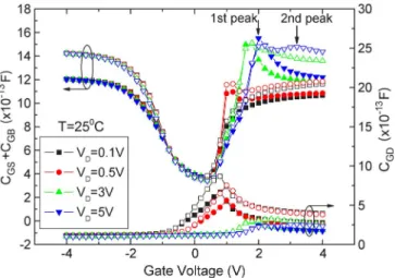
The extracted CGS+ CGB and CGD at room temperature are shown in Fig. 1. At low drain bias (VDS= 0.1 V), both fishbone and ring have the same physical mechanism for the capacitance. The CGS+ CGB presents a similar behavior to the conventional MOSFET. For the lateral nonuniformly doped channel in LDMOS, the drain end will be inverted prior to the source end, resulting in a peak in CGD[7]. Once the gate voltage (VGS) exceeds the threshold voltage (VTH), the CGD starts to fall as the electron charge sheet is no longer connected only to the drain.
By increasing the drain voltage (VDS> 0.5 V), both CGS+
CGB and CGD present peaks. Because the inversion charges may be injected from the intrinsic MOSFET to the depleted area of the drift, the CGDand CGS+ CGBincrease with increasing gate voltages, and the CGS+ CGBeven rises over the limit of 0741-3106/$25.00 © 2008 IEEE
HU et al.: TEMPERATURE-DEPENDENT CAPACITANCE CHARACTERISTICS OF RF LDMOS TRANSISTORS 785
Fig. 1. Extracted CGS+ CGB and CGD versus gate voltage for
differ-ent drain biases. Solid symbols: Fishbone structure. Hollow symbols: Ring structure.
Fig. 2. Schematic view of layout structure and current distribution: (a) fishbone structure and (b) ring structure.
inversion [4]. The CGS+ CGBand CGDreach maximum at the onset of quasi-saturation [12]. Because the higher drain voltage leads to a higher gate voltage at the onset of quasi-saturation, the peaks shift to higher gate voltages.
For the ring structure, however, additional peaks in CGS+
CGBand CGDwere observed when biasing at high drain volt-age (VDS= 5 V) (see Fig. 1). As shown in Fig. 2, the currents flow from drain to source with uniform distribution in the full region of the fishbone structure. However, in the ring structure, the corner region of the drift shows lower current density than
Fig. 3. Extracted CGS+ CGBand CGDversus gate voltage with various
temperatures (a) at drain voltage VDS= 0.1 V and (b) at drain voltage VDS=
5 V for a fishbone structure. The inset shows the drain current versus gate voltage with various temperatures.
the edge region [13], [14], and thus it needs higher gate voltage to enter quasi-saturation. At the first peak, although the edge of the square ring operates in quasi-saturation region, the corner is still in prequasi-saturation. By increasing the gate voltage to 3.2 V, the current in the corner region is high enough to make the velocity of electrons in the drift saturated. Therefore, the corner operates in quasi-saturation and second peaks are generated in the CGS+ CGBand CGD.
Fig. 3 shows the influence of temperature on CGS+ CGBand
CGD of the fishbone structure. At VDS= 0.1 V, the transistor operates in linear region and the temperature dependence of
CGS+ CGB is similar to the conventional MOSFET. With increasing temperature, the threshold voltage decreases and the flatband voltage increases due to higher intrinsic carrier concentration [15]. In our devices, the variation of the threshold voltage with temperature is −1.66 mV/◦C, which equals the shift of the CGDpeak. In addition, the lower threshold voltage at higher temperature also indicates that the source end is in-verted easier. It results in the reduction of CGDwith increasing temperature when the transistor operates in weak and moderate inversion regimes.
At VDS= 5 V, the transistor operates in saturation region, and the temperature coefficients of CGS+ CGBand CGD are positive in weak and moderate inversion regimes, due to the
786 IEEE ELECTRON DEVICE LETTERS, VOL. 29, NO. 7, JULY 2008
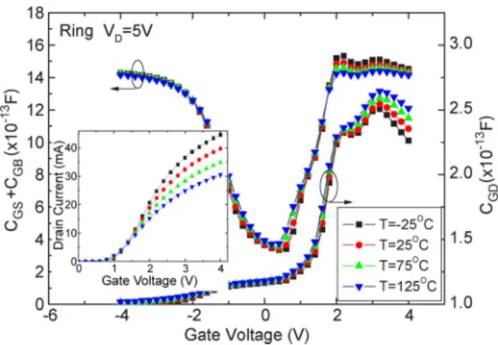
Fig. 4. Extracted CGS+ CGBand CGDversus gate voltage with various
temperatures at drain voltage VDS= 5 V for a ring structure. The inset shows
the drain current versus gate voltage with various temperatures.
reduction of threshold voltage. From Fig. 3(b), we know that the shift of the CGS+ CGB curve at VGS= VTH is about
−1.52 mV/◦C, which approaches the temperature coefficient
of the threshold voltage (∼ −1.64 mV/◦C). At higher gate voltages (VGS> 2 V), the values of capacitances are deter-mined by the onset of quasi-saturation and by the drift depleted region. Because the quasi-saturation current decreases with increasing temperature [see the inset in Fig. 3(b)], the peak value of capacitances decreases. It should be noted that the
CGD shows different behavior with temperature between low and high drain biases when the transistors operate at higher gate voltages (VGS> 2.5 V). At low drain voltage, the CGD is dominated by the accumulation charge which formed below the thin oxide in the drift region and decreases slightly with increasing temperature [see Fig. 3(a)]. At high drain voltages, the CGD now is dominated by the drift depletion capacitance and increases with increasing temperature [see Fig. 3(b)]. Since the temperature variation of capacitance peaks is significantly affected by the drift region, device optimization could be done by changing the drift region length and drift doping concentration.
For the ring structure, the temperature dependence of capac-itances is similar to that of the fishbone structure at VDS= 0.1 V (not shown here). Because the capacitance behavior is mainly related to the threshold voltage at low drain biases, the influence of corners can be neglected. At VDS= 5 V, the temperature coefficients of CGS+ CGBand CGD are positive in weak and moderate inversion regimes, due to the reduction of threshold voltage, as shown in Fig. 4. The shift of the CGS+
CGB curve at VGS= VTH is about −1.42 mV/◦C, which approaches the temperature coefficient of the threshold voltage (∼ −1.56 mV/◦C). At higher gate voltage (VGS> 2 V), the peaks of CGS+ CGB decrease with increasing tempera-ture due to lower quasi-saturation current (see the inset in Fig. 4). However, the peaks of CGD increase with tempera-ture, which is contrary to the trend in a fishbone structure. At the first peak, although the edge of the square ring has been in quasi-saturation region, the corner is still in prequasi-saturation. Therefore, the increase of CGD peak with tem-perature indicates that the temtem-perature-induced variation of
CGD is dominated by the corner. At the second peak, the corner has also been in quasi-saturation region, however, the
CGD in the edge has been dominated by the drift depletion capacitance. Because the drift depletion capacitance is very sensitive to the temperature as indicated in Fig. 3(b), the temperature-induced variation of CGD now is dominated by the edge.
IV. CONCLUSION
The capacitance behaviors of RF LDMOS transistors with different temperatures were investigated. At low drain voltages, the temperature coefficients of CGS+ CGBare positive, while the temperature coefficients of CGDare negative. At high drain voltages, peaks in CGS+ CGB have also been observed and their temperature coefficients are negative. However, the tem-perature coefficients of CGD peaks are negative in a fishbone structure and positive in a ring structure. These observations are important for circuit design to choose a bias condition with lower temperature sensitivity in capacitances. In addition, since the capacitances are affected mainly by the threshold voltage, quasi-saturation current, and drift depletion capacitance, tem-perature effects on these parameters must be considered in the LDMOS capacitance model.
ACKNOWLEDGMENT
The authors would like to thank the staff of United Micro-electronics Corporation for their helpful comments and the staff of High Frequency Technology Center in National Nano Device Laboratories for measurement support.
REFERENCES
[1] F. van Rijs and S. J. C. H. Theeuwen, “Efficiency improvement of LDMOS transistors for base stations: Towards the theoretical limit,” in
IEDM Tech. Dig., Dec. 2006, pp. 11–13.
[2] A. Wood, C. Dragon, and W. Burger, “High performance silicon LDMOS technology for 2 GHz RF power amplifier applications,” in IEDM Tech.
Dig., Dec. 1996, pp. 87–90.
[3] S. Frére, J. Rhayem, H. Adawe, R. Gillon, M. Tack, and A. Walton, “LDMOS capacitance analysis versus gate and drain biases, based on comparison between TCAD simulations and measurements,” in Proc.
IEEE ESSDERC, Sep. 2001, pp. 219–222.
[4] C. Anghel, Y. S. Chauhan, N. Hefyene, and A. Ionescu, “A physical analysis of HV MOSFET capacitance behaviour,” in Proc. IEEE ISIE, Jun. 2005, vol. 2, pp. 473–477.
[5] K. Narasimhulu, M. P. Desai, S. G. Narendra, and V. R. Rao, “The effect of LAC doping on deep submicrometer transistor capacitances and its influence on device RF performance,” IEEE Trans. Electron Devices, vol. 51, no. 9, pp. 1416–1423, Sep. 2004.
[6] R. Valtonen, J. Olsson, and P. De Wolf, “Channel length extraction for DMOS transistors using capacitance–voltage measurements,” IEEE
Trans. Electron Devices, vol. 48, no. 7, pp. 1454–1459, Jul. 2001.
[7] Y. S. Chauhan, F. Krummenacher, C. Anghel, R. Gillon, B. Bakeroot, M. Declercq, and A. M. Ionescu, “Analysis and modeling of lateral non-uniform doping in high-voltage MOSFETs,” in IEDM Tech. Dig., Dec. 2006, pp. 1–4.
[8] Y. S. Chauhan, R. Gillon, M. Declercq, and A. M. Ionescu, “Impact of lateral non-uniform doping and hot carrier degradation on capaci-tance behavior of high voltage MOSFETs,” in Proc. IEEE ESSDERC, Sep. 2007, pp. 426–429.
[9] Y. S. Chauhan, F. Krummenacher, R. Gillon, B. Bakeroot, M. J. Declercq, and A. M. Ionescu, “Compact modeling of lateral nonuniform doping in high-voltage MOSFETs,” IEEE Trans. Electron Devices, vol. 54, no. 6, pp. 1527–1539, Jun. 2007.
HU et al.: TEMPERATURE-DEPENDENT CAPACITANCE CHARACTERISTICS OF RF LDMOS TRANSISTORS 787
[10] H. H. Hu, K. M. Chen, G. W. Huang, C. Y. Chang, Y. C. Lu, Y. C. Yang, and E. Chen, “Characterization of RF lateral-diffused metal–oxide–semiconductor field-effect transistors with different layout structures,” Jpn. J. Appl. Phys., vol. 46, no. 4B, pp. 2032–2036, Apr. 2007. [11] J. Jang, O. Tornblad, T. Arnborg, Q. Chen, K. Banerjee, Z. Yu, and R. W. Dutton, “RF LDMOS characterization and its compact modeling,” in Proc. IEEE MTT-S Int. Microw. Symp. Dig., May 2001, pp. 967–970. [12] C. M. Liu and J. B. Kuo, “Quasi-saturation capacitance behavior of a
DMOS device,” IEEE Trans. Electron Devices, vol. 44, no. 7, pp. 1117– 1123, Jul. 1997.
[13] A. Giraldo, A. Paccagnella, and A. Minzoni, “Aspect ratio calculation in n-channel MOSFETs with a gate-enclosed layout,” Solid State Electron., vol. 44, no. 6, pp. 981–989, Jun. 2000.
[14] R. Giacomini and J. A. Martino, “A simple current model for edgeless SOI nMOSFET and a 3-D analysis,” Solid State Electron., vol. 49, no. 8, pp. 1255–1261, Aug. 2005.
[15] K. M. Chen, G. W. Huang, S. C. Wang, W. K. Yeh, Y. K. Fang, and F. L. Yang, “Characterization and modeling of SOI varactors at various temperatures,” IEEE Trans. Electron Devices, vol. 51, no. 3, pp. 427–433, Mar. 2004.