應用半均等量化及改良式延遲時間補償
連續時間之三角積分調變器
研究生:林永洲
指導教授:洪崇智 博士
應用半均等量化及改良式延遲時間補償
連續時間之三角積分調變器
A Continuous-Time DSM Using Improved Zero-Order loop
Compensation with Semi-Uniform Quantization
研 究 生:林永洲 Student:Yung-Chou Ling
指導教授:洪崇智 Advisor:Prof. Chung-Chih Hung
國 立 交 通 大 學
電 信 工 程 學 系 碩 士 班
碩 士 論 文
A Thesis
Submitted to Department of Communication Engineering College of Electrical Engineering and Computer Science
National Chiao Tung University In Partial Fulfillment of the Requirements
For the Degree of Master In Communication Engineering September 2008 Hsinchu, Taiwan
中華民國九十七年九月
應用半均等量化及改良式延遲時間補償
連續時間之三角積分調變器
學生:林永洲
指導教授
:洪崇智
國立交通大學電信工程學系碩士班
摘
要
隨著無線通訊的蓬勃發展,應用於無線通訊中的類比數位轉換器也受到更 多的矚目。在所有的類比數位轉換器的架構中,三角積分 ( Delta-sigma ) 類比 數位轉換器優於快閃 ( Flash ) 和導管式 ( Pipeline ) 類比數位轉換器的地方, 在於擁有較佳的頻寬和解析度的經濟效益。近年來,由於有著更低的功率消耗 及較大的訊號頻寬,連續時間三角積分類比數位轉換器比起離散時間三角積分 類比數位轉換器更為廣泛應用於無線通訊中。 在此篇論文中,我們著重於連續時間三角積分調變器的設計概念,且實現 一1 MHz 訊號頻寬,並具有 60 dB 動態範圍 ( Dynamic Range ) 及最大訊號雜 訊失真比 ( SNDR ) 為 59.6 dB 的電路,此電路使用電阻取代原先轉導當作零點 轉移的功用,以節省面積和功率。此外,我們也提出另一架構,此電路具有2MHz 的訊號頻寬及最大訊號雜訊失真比63 dB 且使用改良式延遲時間補償及半均等 量化的技巧來節省面積和功率。 晶片分別以台積電180 奈米互補式金氧半導體製程及 130 奈米互補式金氧 半導體製程所製造。量測結果顯示第一顆晶片操作在100 MHz 取樣頻率下,消
耗13.7 mW 的功率在 1.8 V 的供應電壓下。模擬結果顯示另一顆晶片操作在 62.5 MHz 取樣頻率下,消耗 10 mW 的功率在 1.2 V 的供應電壓下。
A Continuous-Time DSM Using Improved Zero-Order loop
Compensation with Semi-Uniform Quantization
Student:Yung-Chou Ling
Advisors:Dr.
Chung-Chih Hung
Department of Communication Engineering
National Chiao Tung University
ABSTRACT
With the growth of wireless communication, there has been more focus on the analog-to-digital converter (ADC) for wireless applications. Among all of ADCs, delta-sigma converters are preferable over flash and pipeline converters because they offer the most economic bandwidth and accuracy trade-off. Recently, continuous-time delta-sigma ADCs get growing interests in wireless applications for their lower power consumption and wider bandwidth as compared with the discrete-time counterparts.
In this thesis, it focuses on the design procedure of the continuous-time delta-sigma modulator and the first chip is presented to achieve 60 dB dynamic range and 59.6 dB SNDR within a 1MHz signal bandwidth. This work replaces the transconductor with resistors as the function of zero shifts to save chip area and power consumption. Besides, we also show the other architecture to achieve 63 dB SNDR within a 2MHz signal bandwidth and this work uses the techniques of improved zero-order loop compensation and semi-uniform quantization to save chip
area and power consumption.
The first chip has been fabricated by TSMC 180 nm CMOS process and the other has been fabricated by TSMC 130 nm CMOS process. The test results show that the first work consumes 13.7 mW with 100 MHz sample rate in 1.8 V supply voltage. The simulation results show that the other work consumes 10 mW with 62.5 MHz sample rate in 1.2 V supply voltage.
誌
謝
隨著這份碩士論文的完成,兩年來在交大的求學生涯也跟著告一個段落,往 後迎接著我的,又是另一段嶄新的人生旅程。本論文得以順利完成,最先要感謝 的,當然是我的指導教授洪崇智老師。這兩年的研究生涯中,給予我無微不至的 指導與照顧,且讓我在研究主題上有無限的發展空間。而類比積體電路實驗室所 提供完備的軟硬體資源,讓我在短短兩年碩士班研究中,學習到如何開始設計類 比積體電路,乃至於量測電路,甚至單獨面對及思考問題的所在。此外要感謝李 育民教授和溫宏斌教授撥冗擔任我的口試委員並提供寶貴意見,使得本論文更為 完整。也感謝國家晶片系統設計中心提供先進的半導體製程,讓我有機會將所設 計的電路加以實現並完成驗證。 另一方面,要感謝所有類比積體電路實驗室的成員兩年來的互相照顧與扶 持。首先,感謝博士班的學長薛文弘、羅天佑、黃哲揚以及已畢業的碩士班學長 白逸維、林明澤、高正昇、邱建豪、吳國璽和廖德文在研究上所給予我的幫助與 鼓勵。特別是文弘學長,由於他平時不吝惜的賜教與量測晶片時給予的幫助,使 得我的論文研究得以順利完成,對於他的無私幫助,我沒齒難忘。另外我要感謝 郭智龍、夏竹緯、楊文霖、邱楓翔、黃介仁和張維欣等諸位同窗,透過平日與你 們的切磋討論,使我不論在課業上,或研究上都得到了不少收穫。尤其是工四718 實驗室的同學們,兩年來陪我ㄧ塊兒努力奮鬥,一起渡過那段同甘共苦的日子, 也因為你們,讓我的碩士班生活更加多采多姿,增添許多快樂與充實的回憶。此 外也感謝學弟們李尚勳、黃聖文、許新傑和簡兆良的熱情支持,因為你們的加入, 讓實驗室注入一股新的活力與朝氣,我祝你們研究順利。 到這邊,特別要致上最深的感謝給我的父母及家人們,感謝你們從小到大所 給予我的栽培、照顧與鼓勵,讓我得以無後顧之憂地完成學業,朝自己的理想邁 進,我要謝謝你們給我那麼那麼多的愛和付出,我會一輩子記在心理;還有默默 陪伴我的女友,感謝妳體諒我平時的忙碌,以及給我很多很多的關懷,且在這段 成長的路上與我相伴。 最後,所有關心我、愛護我和曾經幫助過我的人,願我在未來的人生能有 一絲的榮耀歸予你們,謝謝你們。 林永洲 于 交通大學工程四館 718 實驗室 2008.9.05
Table of Content Abstract List of Figures List of Tables
Chapter 1
Introduction………..1
1.1 Motivation…...1 1.2 Thesis Overview…...2Chapter 2
Overview of Oversampling ΔΣ ADC…………..……….4
2.1 Sampling and Quantization...4
2.2 Oversampling………...9
2.3 Noise Shaping…...10
2.3.1 First order Delta-Sigma Modulator…………..………...11
2.3.2 Second order Delta-Sigma Modulator……..………...14
2.3.3 High order Delta-Sigma Modulator...16
Chapter 3
Design of Continuous-Time ΔΣ modulator
……….…...183.1 DT to CT Conversion of ΔΣ Modulator……….………18
3.1.1 Impulse-Invariant Transformation……….……...18
3.1.2 Synthesis of CT ΔΣ Feedback DAC……….……...20
3.2 Non-idealities in ΔΣ Modulator…………...……….……..………21
3.2.1 Non-idealities in CT Integrators……….………...21
3.2.2 Finite OpAmp Gain and Gain-Bandwidth………...24
Table of Content
3.2.4 Clock Jitter………..…..…...27
3.2.5 Element Mismatch in a Multi-bit DAC…………..………...30
Chapter 4
A Continuous-Time Delta-Sigma Modulator Using Feedback
Resistors…...…31
4.1 System Level Design.……..……….….…….………31
4.2 Architecture of the Loop Filter……….….…….………33
4.2.1 NTF Zero Optimization……….………33
4.3 System Level Simulation………..………….……….34
4.4 Circuit Level Design…..………..………….……….35
4.4.1 Loop Filter……….………...35
4.4.2 First Stage - Active-RC Integrator………...36
4.4.3 Following Stage - Gm-C Transconductor……….………40
4.4.4 Feedback Resistors………..…..…...42
4.4.5 Tuning Circuit……….…………..………...43
4.4.6 Low Jitter Clock Generation………….…………..………...44
4.5 Circuit Level Simulation………..………….……….45
Chapter 5
A Continuous-Time DSM with Improved Zero-Order Loop
Compensation and Semi-Uniform Quantization...47
5.1 System Level Design.……..……….….…….………47
5.2 Architecture of the Loop Filter……….….…….………48
5.2.1 Out-of-Band Quantization Gain………48
5.2.2 Improved Zero-Order Loop Compensation………...50
5.2.3 Non-Uniform Quantization……….………..53
5.2.4 Dynamic Element Matching………..55
Table of Content
5.4 Circuit Level Design…..………..………….……….59
5.4.1 Loop Filter……….………...59
5.4.2 First Stage - Active-RC Integrator………...60
5.4.3 Following Stage - Gm-C Transconductor……….………62
5.4.4 Current Steering DAC with Semi-Uniform Quantization…………...64
5.4.5 Current Summation Circuit………..………..………...66
5.5 Circuit Level Simulation………..………….……….67
Chapter 6
Setup and Experimental Results……….……...69
6.1 A Continuous-Time Delta-Sigma Modulator Using Feedback Resistors………...69
6.1.1 Test Setup……….………70
6.1.2 Measurement Results……….………...71
6.1.3 Comparison between this work and reported designs………...72
6.2 A Continuous-Time DSM with Improved Zero-Order Loop Compensation and Semi-Uniform Quantization………..…..………….……….………74 6.2.1 Test Setup……….………74 6.2.2 Measurement Results………...……….75
Chapter 7
Conclusions……...………..…….……...77
7.1 Conclusions………...………..………...77 7.2 Future Works..……...………..………...78Bibliography
………....……….………...79List of Figures
Fig. 1.1 The transconductance range ...2
Fig. 2.1 The sampling spectral ...5
Fig. 2.2 Analog-to-digital conversion ...5
Fig. 2.3 (a) Transfer curve and (b) error function of a 4-level quantizer...7
Fig. 2.4 (a) Probability density function of quantization noise (b) power spectral density of quantization noise ... 8
Fig. 2.5 Oversampling...9
Fig. 2.6 (a) A general noise-shaping delta-sigma modulator (b) Linear model of the modulator showing injected quantization noise... 10
Fig. 2.7 The block diagram of the first-order low-pass delta-sigma modulator ... 11
Fig. 2.8 First-order delta-sigma modulator ...12
Fig. 2.9 The block diagram of the second-order low-pass ΔΣ modulator...14
Fig. 2.10 Different order noise shaping curves...16
Fig. 2.11 Empirical SQNR limit for 1-bit modulators of order N ...17
Fig. 3.1 The loop filter representation for (a) DT modulator and (b) CT modulator...19
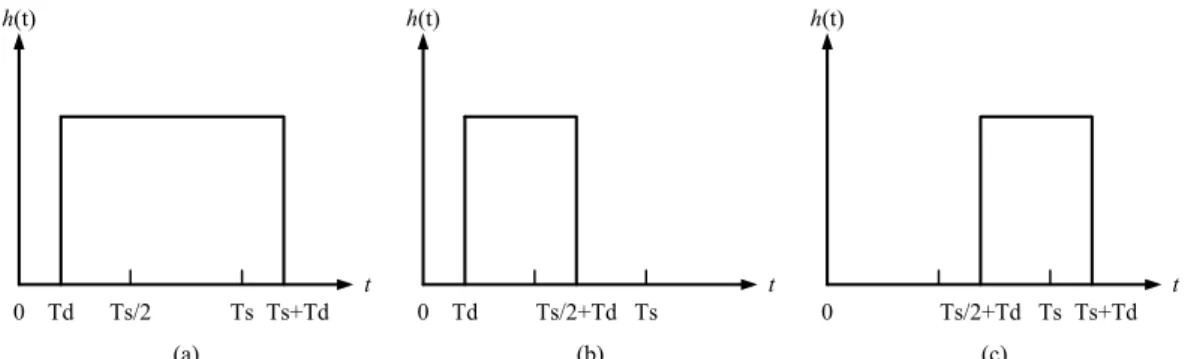
Fig. 3.2 DAC feedback impulse response (a) NRZ (b) RZ (c) HRZ ...20
Fig. 3.3 (a) Active-RC (b) Gm-C integrators...21
Fig. 3.4 The GBW requirement of the OpAmp in the integrator...22
Fig. 3.5 The active-RC integrator with single pole OpAmp...24
Fig. 3.6 DAC feedback impulse response including Excess Loop Delay (a) NRZ (b) RZ (c) HRZ ... 26
Fig. 3.7 Continuous-Time ΔΣ modulator with zero-order loop compensation...27
Fig. 3.8 Single-bit NRZ, RZ and HRZ DAC feedback pulse with jitter noise ...28
Fig. 3.9 Multi-bit NRZ, RZ and HRZ DAC feedback pulse with jitter noise ...29
Fig. 4.1 Simulated SNR as a function of out-of-band-gain for single bit...32
Fig. 4.2 Optimal third-order NTF for OSR = 50...33
Fig. 4.3 The architecture of CT ΔΣ modulator using feedback resistors ...34
Fig. 4.4 The system simulation of CT ΔΣ modulator using feedback resistors ...34
List of Figures
Fig. 4.6 Schematic of gain-boosting folded-cascode OpAmp ...36
Fig. 4.7 The spice simulation, including DC gain and phase margin ...37
Fig. 4.8 Schematic of CMFB circuit...38
Fig. 4.9 Schematic of Gm with source degeneration resistor ...40
Fig. 4.10 The simulated transconductance range...40
Fig. 4.11 The spice simulation, including DC gain and phase margin ...41
Fig. 4.12 The simplified schematic of loop filter...42
Fig. 4.13 Tunable capacitor array ...43
Fig. 4.14 Schematic of low jitter clock generation ...44
Fig. 4.15 The circuit simulation of this work using feedback resistors ...45
Fig. 4.16 Chip photo of this work using feedback resistors...46
Fig. 5.1 Noise transfer function amplitude of a ΔΣ modulator ...48
Fig. 5.2 Simulated SNR as a function of Qmax for different quantization bit third order ΔΣ modulators (OSR = 16)... 49
Fig. 5.3 Continuous-Time ΔΣ modulator architecture with compensation loop...50
Fig. 5.4 Realization of the zero-order loop feedback path...52
Fig. 5.5 The transfer curve of semi-uniform quantization ...53
Fig. 5.6 The quantization error of semi-uniform quantization...54
Fig. 5.7 Unit element DAC with randomized element selection ...55
Fig. 5.8 The architecture of CT ΔΣ modulator we propose ...56
Fig. 5.9 The simulation of DC gain in first active-RC integrator ...57
Fig. 5.10 The simulation of HD3 in the first active-RC integrator...57
Fig. 5.11 The simulation of DC gain in the second Gm-C integrator...57
Fig. 5.12 The simulation of HD3 in the second Gm-C integrator ...58
Fig. 5.13 The system simulation of CT ΔΣ modulator we propose ...58
Fig. 5.14 Simplified block diagram of the third-order CT ΔΣ modulator...59
Fig. 5.15 Schematic of folded-cascode OpAmp ...60
Fig. 5.16 The spice simulation, including DC gain and phase margin ...61
Fig. 5.17 Schematic of Gm with source degeneration resistor ...62
Fig. 5.18 The simulated transconductance range...62
Fig. 5.19 The spice simulation, including DC gain and phase margin ...63
Fig. 5.20 Schematic of the unit current steering DAC cell...64
List of Figures
Fig. 5.22 Schematic of the current summation circuit ...66
Fig. 5.23 The circuit simulation of this work (16384pt, 156 kHz input) ...67
Fig. 5.24 Chip photo of this work ...68
Fig. 6.1 Die photo of this work using feedback resistors...69
Fig. 6.2 Test environment ...70
Fig. 6.3 Photograph of the first test board ...71
Fig. 6.4 Output spectrum of this work (a) post-simulation (b) measured...71
Fig. 6.5 Dynamic ranges of this work using feedback resistors ...72
Fig. 6.6 Die photo of this work we propose...74
Fig. 6.7 Photograph of the second test board...75
Fig. 6.8 Output spectrum of this work ...76
List of Tables
Table 3.1 Overview of various advantages and drawbacks of various CT integrator
approaches...23
Table 4.1 Summary of spice simulation results ...37
Table 4.2 Summary of spice simulation results ...41
Table 4.3 Summary of circuit level simulation results...46
Table 5.1 Summary of spice simulation results ...61
Table 5.2 Summary of spice simulation results ...63
Table 5.3 Summary of circuit level simulation results...68
Table 6.1 Summary of measured results ...72
1.1 Motivation
Delta-Sigma AD converters can achieve both high resolution and high linearity for low bandwidth applications, such as audio signal processing. Among all the ΔΣ converters (discrete-time (DT) and continuous-time (CT)), DT modulators are less suitable for high speed conversions. Because of the settling time requirement for the charge transfer between the switched-capacitor integrators, it boosts its power consumption. Therefore, they are used for low bandwidth applications. On the contrary, the sampling speed in CT isn’t limited by any settling requirements. Besides, there is no need for sample-and-hold circuit in the front-end and benefit from having inherent anti-aliasing filter. This leads to lower power consumption and less chip area. However, CT modulators suffer from the severe process-varying RC time constant, excess loop delay and clock jitter issues which require extra care.
As the IC technologies advanced, it resulted in lower power supply voltages, which caused the input range of the transconductor decrease and made the dynamic range of ΔΣ modulators decrease sorely, as presented in Fig. 1.1. To overcome this problem, improved ΔΣ modulator architecture is proposed. This architecture achieves high out of-band gain and use improved zero-order loop compensation with semi-uniform quantization.
Fig. 1.1 The transconductance range
1.2 Thesis Overview
This thesis covers theoretical analysis of the CT ΔΣ modulator and the method of the CT loop filter from its DT function. After discussing the design issues of the CT ΔΣ modulator as well as the solutions, the detailed design procedure of the prototype modulator are presented. The thesis is organized as following:
Chapter 2 reviews some basic concepts about ΔΣ ADCs to help understand the rest of the thesis.
Chapter 3 describes the equivalence between the DT and CT loop filters in terms of impulse-invariant transformation (IIT). Besides, effects of various non-idealities and potential solutions to deal with them are discussed.
Chapter 4 proposes a CT ΔΣ modulator using feedback resistors. The system level design procedure which combines many aspects of the design considerations and detailed circuit level design are discussed.
level design procedure which combines many aspects of the design considerations and circuit design of this CT ΔΣ modulator.
Chapter 6 covers the issues of test board design as well as the chip evaluation work.
In this chapter, we describe some basic background knowledge about ΔΣ ADCs. The concepts of quantization, oversampling and noise-shaping are introduced and illustrated with examples. The tradeoffs of the various sigma-delta modulator architectures will be discussed.
2.1 Sampling and Quantization
In order to properly interface the analog world which is composed of continuous-time signal (e.g. voice, audio or video) with the digital signal processor which can only process discrete-time signal, analog-to-digital conversion is required. We describe it into two basic operations: uniform sampling in time and quantization in amplitude.
Under the assumption that the signal information of the continuous input waveform u t is contained in the signal band, i.e.,( ) fs i g £ fB , where f is B defined as the signal bandwidth, the sampling in time is a completely invertible process. This is easily understood when considering a quantization in time as a periodization in frequency [1], which is illustrated in Fig. 2.1. There, the considered input signal is sampled at uniform time intervalsT , the sampling time, or with a S
Fig. 2.1 The sampling spectral
spectrum at multiples of f . From Fig. 2.1 it is obvious that by sample low-pass S filtering, the original base-band spectrum can be reconstructed, provided that the sampling itself does not result in overlap or aliased regions. This is achieved when:
2
S B N
f ³ f = f (2.1) which is known as the Nyquist theorem, where fN is the Nyquist frequency. To assure a proper sampling operation, the condition in (2.1) is enforced by an analog filter preceding the sampling operation, called the antialiasing filter (AAF).
a
fS fS
The basic ADC structure is shown in Fig. 2.2. An ADC working with a sampling frequency of fN is called a Nyquist Rate converter. But in real implementations, this results in a zero transition band for the filter to cut off the unwanted high frequency signals, making it hard to design. On the other hand, analog filters with a gentle roll in their transition band are less costly, easier to design; require less power, and smaller chip area while introducing less phase distortion. Therefore, many ADCs work with sampling rates higher than fN , and one defines: 2 S N f O S R f = (2.2) as the oversampling ratio of the ADC.
The process of quantization in amplitude, usually referred to as the quantization, encodes a continuous range of analog values into a set of discrete levels. The quantizer is assumed to be a memoryless nonlinear device completely defined by its static input-output characteristics, i.e., by its y-v transfer curve. An example of such a curve is shown in Fig. 2.3(a), where the number of quantization level is 4 which can be represented by a 2-digit binary code, and the difference of two adjacent quantized values Δ is the same as the difference between input thresholds, also known as least-significant bit size or LSB size, given by VLSB. The difference
between the lowest and the highest levels is called the full-scale (FS) of the quantizer, given by 2VRef. The deviation between the sampled input and the
quantized output is called the quantization error, or the quantization noise. Fig. 2.3(b) shows the relationship between the quantization noise q and the input y. From this figure, it can be seen that as long as y is between –( VRef + VLSB/2 ) and +( VRef +
VLSB/2 ), the error q is between -VLSB/2 and +VLSB/2. The range of y where this
quantization step as well as the LSB size is given by Δ = VLSB =FS/(2N-1), which
is in the case 2VRef /3.
The ideal quantizer is a deterministic device. The output v and hence the error q are fully determined by the input y. However, under certain circumstances, for example, if the input y stays within the non-overload input range of the quantizer, and changes by sufficiently large amounts from sample to sample so that its position within a quantization interval is essentially random, then it is permissible to assume
v
y
Ref Ref LSBy
q=v-y
Ref Ref +VLSB/2 -VLSB/2Fig. 2.3 (a) Transfer curve and (b) error function of a 4-level quantizer
that q is a white noise process with samples uniformly distributed between - VLSB/2 and +VLSB/2. The probability density function (PDF) and power spectral
Fig. 2.4 (a) Probability density function of quantization noise (b) power spectral density of quantization noise
The impact of the quantization noise on the ADC’s performance can be found by calculating its maximum signal-to-quantization-noise ratio (SQNR). This parameter is obtained by dividing the power of a sinusoidal input signal by the power of the quantization noise. The power of a sinusoidal signal is given by Amp2/2, where Amp is the amplitude of the signal. The power of the quantization noise is given in (2.3). 2 / 2 2 2 / 2 1 1 2 L S B L S B V q V L S B q d q V s -D =
ò
= (2.3)To get the SQNR, Amp should be equal to half of the non-overload input range of the quantizer, which is VRef+VLSB/2.
(
)
2 2 1 R e 2 2 2 2 2 3 2 2 2 2 1 2 1 2 N f N V S Q N R -D æ + ö ç ÷ D è ø = = = D D (2.4)(2.4) is expressed in dB, this becomes (2.5), which is widely used to assess the performance of the data converter.
1 0
[ ] 1 0 l o g 6 . 0 2 1 . 7 6
2.2 Oversampling
A way to calculate the power of the quantization noise is to integrate the power spectral density over the full bandwidth which we interest:
2 2 / 2 2 / 2 1 1 2 1 2 S S f q f S d f f s -D D =
ò
= (2.6)From above equation, it is obvious that if the bandwidth of interest is much lower than the bandwidth which we interest, the resolution of the ADC can be improved by filtering the output to the desired bandwidth which reduces the total power of the quantization noise. This technique, illustrated in Fig. 2.5, is called oversampling.
f
PSD0
f
Bf
S/2
Noise Signal Band Filtered Noise Fig. 2.5 OversamplingNow, the power of the in-band quantization noise is given in (2.7). 2 2 1 S 2 2 2 S f q B q f q q S S f N d f f f O S R s s s -=
ò
= = (2.7)where OSR, defined as 2
S B
f
f , is called oversampling ratio which is one of the most important parameters used to characterize the oversampling data converters. The power of input signal is not modified since it is assumed that it has no frequency content above f . Therefore, the maximum SQNR is given by: B
[ ] 6 . 0 2 1 . 7 6 1 0 l o g
S Q N R d B = N + + O S R (2.8)
It is obvious that if the sampling rate is equal to twice the Nyquist rate (OSR = 2), the SQNR is improved by 3 dB. (2.8) shows that oversampling can improve the SQNR with the OSR at a rate of 3 dB/octave, or 0.5 bit/octave [2].
2.3 Noise Shaping
In the previous section, we show that oversampling can be used to trade speed for resolution of ADC. It is noticed that the quantization noise in previous section has a flat power spectral density over the full bandwidth [- fS / 2 , fS / 2 ] . A more efficient way to use oversampling is to shape the spectral density such that most of the quantization noise power is outside the band of interest. A general noise-shaped sigma-delta modulator and its linear model have been shown in Fig. 2.6.
Fig. 2.6 (a) A general noise-shaping delta-sigma modulator (b) Linear model of the modulator showing injected quantization noise
Treating the linear model shown in Fig. 2.6 as having two independent inputs, ( )
u n and e n , we can derive a signal transfer function ( ) S T F z , and a ( )
( ) ( ) ( ) ( ) 1 ( ) Y z H z S T F z U z H z = = + (2.9) ( ) 1 ( ) ( ) 1 ( ) Y z N T F z E z H z = = + (2.10) According to (2.9) and (2.10), the zeros of the noise transfer function
( )
N T F z , will be equal to the poles of H ( )z . In other words, we can control
the zeros of the noise transfer function by choosing the function of the loop filter. We can also using super position to combine two signals, and find out the output as
( ) ( ) ( ) ( ) ( )
Y z = S T F z U z + N T F z E z (2.11)
The S T F z generally have all-pass or low-pass frequency response and ( )
the N T F z( ) have high-pass frequency response. In other words, the
( )
S T F z will be approximately unity over the signal band and the
( )
N T F z will be approximately zero over the same frequency band. The
quantization noise will be removed to high frequency band when using noise-shaping strategy [3]. The quantization noise over the frequency band which we interest will be reduced and do not affect the input signal. This would improve the SNR significantly for overall system.
2.3.1 First-Order Delta-Sigma Modulator
x
Quantizer
y
In Fig. 2.7, it is a block diagram of the first-order low-pass delta-sigma modulator. It includes an integrator and a quantizer. The input of the integrator is the input signal minus the output signal of the modulator through the DAC. In this example, since the loop filter is a high-pass filter, the noise function should have a zero at dc (i.e., z = 1). The transfer function of the discrete-time integrator (i.e., have a pole at z = 1) is 1 ( ) 1 H z z = - (2.12) Its block diagram for such a choice is shown in Fig. 2.8.
Fig. 2.8 First-order delta-sigma modulator
According to (2.9) and (2.10), we can obtain the signal transfer function ( ) S T F z , is given by 1 1 ( ) 1 ( ) 1 ( ) 1 1 Y z z S T F z z U z z -= = = + (2.13)
and the noise transfer function N T F z , is given by ( )
1 ( ) 1 ( ) 1 1 ( ) 1 1 Y z N T F z z E z z -= = = -+ (2.14)
Combining the two signal transfer function, we can obtain the output as
1 1
( ) ( ) (1 ) ( )
Y z = z U- z + - z- E z
(2.15) We see that the input signal is just a delay through the input to the output, and the quantization noise is through a discrete-time differentiator (i.e., a high-pass filter) to the output. We are interesting in the magnitude of the noise transfer function,
( )
N T F f , we let z = e jwT = e j2p f / fS and get the following:
2 / ( ) 1 j f fS N T F f = - e- p / / / 2 2 S S S j f f j f f j f f e e j e j p p p -= ´ ´ / s i n 2 j f fS S f j e f p p -æ ö = ç ÷ ´ ´ è ø (2.16)
Taking the magnitude of both sides, we have the high-pass function
( ) 2 s i n ( ) S f N T F f f p = (2.17)
Now we can integrate the quantization noise power over the frequency bandwidth we interest as below
2 2 ( ) ( ) B B f e f e P S f N T F f d f -=
ò
2 2 1 2 s i n 1 2 B B f f S S f d f f f p -é æ öù æ D ö = ç ÷ ê ç ÷ú è ø ë è øûò
(2.18)When fB = fS (i.e., OSR>>1), we can approximate s i n ( )
S f f p to be ( ) S f f p , so we have 3 3 2 2 2 2 2 1 1 2 3 3 6 B e S f P f O S R p æ ö p æ D ö æ ö D æ ö @ ç ÷ ç ÷ ç ÷ = ç ÷ è ø è ø è ø è ø (2.19)
Now we can estimate the maximum SNR by assuming the input signal having maximum amplitude. We can obtain as
2 3 2 3 3 1 0 l o g ( ) 1 0 l o g 2 1 0 l o g ( ) 2 N S E P S N R O S R P p æ ö é ù = = ç ÷ + ê ú è ø ë û (2.20) or, equivalently, 6 . 0 2 1 . 7 6 5 . 1 7 3 0 l o g ( ) S N R = N + - + O S R (2.21)
We can see that the first-order noise shaping can give an SNR improvement for 9 dB or 1.5 bits by doubling the OSR. This result should be compared to the 0.5 bits/octave when oversampling with no noise shaping.
2.3.2 Second-Order Delta-Sigma Modulator
Fig. 2.9 The block diagram of the second-order low-pass ΔΣ modulator
The second-order low-pass delta-sigma modulator is shown in Fig. 2.9. Through the arrangement of the block diagram, we can obtain the noise transfer function N T F ( f ) , as a second-order high-pass function
1 2
( ) (1 )
N T F f = - z - (2.22)
and the signal is just a delay to output. The signal transfer function is given by 1
( )
S T F f = z
(2.23) Combining the two signal transfer function, we can obtain the output as
1 1 2
( ) ( ) (1 ) ( )
The same as before, we interest in the magnitude of the noise transfer function can be show to given by
2 ( ) 2 s i n ( ) S f N T F f f p é ù = ê ú ë û (2.25)
Integrating the quantization noise power over the frequency band which we interest and using the approximation, we can get the result:
2 2 ( ) ( ) B B f e f e P S f N T F f d f -=
ò
4 2 1 2 s i n 1 2 B B f f S S f d f f f p -é æ öù æ D ö = ç ÷ ê ç ÷ú è ø ë è øûò
5 5 2 4 2 2 4 1 1 2 5 6 0 B S f f O S R p æ ö p æ D ö æ ö D æ ö = ç ÷ ç ÷ ç ÷ = ç ÷ è ø è ø è ø è ø (2.26)Again, assuming the maximum signal power is used, the maximum SNR for this case is given by
2 5 4 3 5 1 0 l o g ( ) 1 0 l o g 2 1 0 l o g ( ) 2 N S E P S N R O S R P p æ ö é ù = = ç ÷ + ê ú è ø ë û (2.27) or, equivalently, 6 . 0 2 1 . 7 6 1 2 . 9 5 0 l o g ( ) S N R = N + - + O S R (2.28)
We can see that the second-order noise shaping can give an SNR improvement for 15 dB or 2.5 bits by doubling the OSR.
Fig. 2.10 shows the noise-shaping curves compared with shape of zero-, first-, second- and third-order. The noise power decreases as the noise-shaping order increases over the band which we interest. But the out-of-band noise power increases for the higher-order modulators.
0 0.1 0.2 0.3 0.4 0.5 0 1 2 3 4 5 6 7 8 M agn itude Normalized Frequency Noise shaping Function
Fig. 2.10 Different order noise shaping curves
2.3.3 High-Order Delta-Sigma Modulator
As mentioned before, we extend the delta-sigma modulator to L order, and get the noise transfer function
1
( ) (1 )L
N T F f = - z - (2.29)
We let z = e jwT = e j2p f / fS and get the magnitude response 2 ( ) 2 s i n ( ) S f N T F f f p é ù = ê ú ë û (2.30)
Integrating the quantization noise power over the frequency band which we interest and using the approximation, we can get the result:
2 2 ( ) ( ) B B f e f e P S f N T F f d f -=
ò
2 2 1 2 s i n 1 2 B B L f f S S f d f f f p -é æ öù æ D ö = ç ÷ ê ç ÷ú è ø ë è øûò
Second order Third order First order No noise shaping2 1 2 1 2 2 2 2 2 1 1 2 2 1 1 2 ( 2 1 ) L L L L B S f L f L O S R p æ ö + p + æ D ö æ ö D æ ö = ç ÷ ç ÷ ç ÷ = ç ÷ + + è ø è ø è ø è ø g (2.31) Again, assuming the maximum signal power is used, the maximum SNR for this case is given by
2 2 1 2 3 2 1 1 0 l o g 2 1 0 l o g ( ) 2 N L L L S N R O S R p + + æ ö é ù = ç ÷ + ê ú è ø ë û (2.32) or, equivalently, 2 6 . 0 2 1 . 7 6 ( 2 0 1 0 ) l o g 1 0 l o g ( ) 2 1 L S N R N L O S R L p = + + + -+ (2.33) In general case, the SNR will improve with the OSR at a rate of 6L+3 dB/octave, or equivalently, L+0.5 bit/octave with the L-order noise shaping. Fig. 2.11 shows the SQNR tradeoff between order and OSR.
4 8 16 32 64 128 256 0 20 40 60 80 100 120 140 160 P ea k S QNR ( d B) OSR N = 1 N = 2 N = 3 N = 4 N = 5
In this chapter, we illustrate the procedure to choose the feedback DAC pulse shapes and design the loop filter function for CT ΔΣ modulator. Besides, various non-idealities will affect the performance, even the stability of the CT ΔΣ modulator. These non-idealities, including finite OpAmp gain and gain-bandwidth, excess loop delay, element mismatch in the multi-bit feedback DAC and clock jitter, would be analyzed in detail.
3.1 DT to CT Conversion of ΔΣ Modulator
3.1.1 Impulse-Invariant Transformation
The quantizer in a CT ΔΣ modulator is clocked, that is, there is an implicit sampling action inside the modulator. Because sampled circuits are DT circuits, we can make the sampling explicit by placing the sampler immediately prior to the quantizer without changing the behavior of the modulator, as Fig. 3.1 shown. As mentioned above, the two modulators are equivalent if their quantizers have the same inputs at each sampling instant, which means
( ) ( ) |
S
C t n T
x n = x t = (3.1)
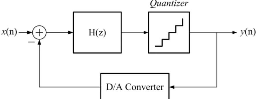
H(z) D/A Converter x(n) Quantizer y(n) q(n) H(s) D/A Converter x(n) Quantizer y(n) q(t) q(n) y(t) y(n) Fs D/A Converter H(z)
y(n) u(n) y(n) D/A Converter y(s) H(s) u(n)
DAC(s)
q(t) Fs
(a) (b)
Fig. 3.1 The loop filter representation for (a) DT modulator and (b) CT modulator
This can be satisfied if the open loop impulse responses are the same at sampling instants, which can be written as
{
}
{
}
1 ( ) 1 ( ) ( ) | S t n T H z L D A C s H s - -= = (3.2)In the time domain, this leads to the condition
( ) ( ) ( ) |
S
t n T
h n = D A C t * h t = (3.3)
where h n , ( ) D A C t and ( ) h t are the impulse responses of the DT ( ) loop filter H ( )z , the CT feedback DAC and the CT loop filter H ( )s , respectively. This transformation between the DT and CT domains is called the
Impulse Invariant Transformation [4], because it makes the open loop impulse
(a) 0 Ts t h(t) (b) 0 Ts t h(t) Ts/2 (c) 0 Ts t h(t) Ts/2 Ts/2
Fig. 3.2 DAC feedback impulse response (a) NRZ (b) RZ (c) HRZ
3.1.2 Synthesis of CT ΔΣ Feedback DAC
To actually perform the Impulse Invariant Transformation, the continuous-time DAC feedback pulse shape has to be decided first. Different pulse shapes result in different transformations between the DT and CT modulators. We will shortly discuss their practical advantages. There are three commonly used rectangular DAC feedback pulses: non-return-to-zero (NRZ), return-to-zero (RZ) and half-delay-return-to-zero (HRZ) [5]. Their impulse responses are shown in Fig. 3.2. DACs with NRZ shapes provide constant output over a full period; DACs with RZ shapes produce constant valid output only from 0 to T/2 and DACs with HRZ produce a half clock cycle delayed version of RZ. The transfer function of NRZ, RZ and HRZ can be described by the same equation:
e x p ( ) e x p ( ) ( ) D A C s s H s s a b - - -= (3.4)
where α and β are valid feedback starting and ending times respectively, so we have
0 , 0 , 0 . 5 0 . 5 , S S S S T N R Z T R Z H R Z T T a b a b a b = = ì ï = = í ï = = î (3.5)
After determining the DAC feedback pulse shape and its transfer function, the impulse invariant transform can be executed following the steps below. At first, we will write H ( )z as a partial fraction expansion. Following, we convert each
partial fraction from z-domain to s-domain. At the last, we recombine the results from step 2 to get H C ( )s [6].
3.2 Non-idealities in ΔΣ Modulator
3.2.1 Non-idealities in CT Integrators
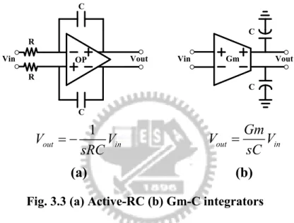
Gm OP C C C C R RVin Vout Vin Vout
1
out inV
V
sRC
= -
out inGm
V
V
sC
=
Fig. 3.3 (a) Active-RC (b) Gm-C integrators
The basic circuit blocks of a CT loop filter are the CT integrators. Many kinds of CT integrators are available but the most commonly used are active-RC integrators and Gm-C integrators, as shown in Fig. 3.3.
The advantages of the active-RC integrators over the Gm-C counterparts include higher linearity and larger input signal swing. Because the active-RC integrators are based on the closed loop applications of the operational amplifiers (OpAmps), the OpAmp’s inputs are virtual ground and only experience very small signal swing regardless of the integrator’s input. On the contrary, the transconductor, which performs voltage-to-current (V-I) transformation with a known
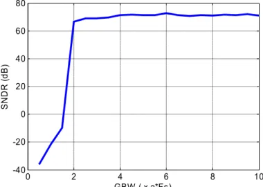
0 2 4 6 8 10 -40 -20 0 20 40 60 80 SNDR ( dB) GBW ( x a*Fs)
Fig. 3.4 The GBW requirement of the OpAmp in the integrator
transconductance, operates under the open-loop condition in the Gm-C integrators, so its inputs have to experience the full swing of the integrator’s input, which degrades the linearity of the integrator. Due to this reason, the input signal of the Gm-C integrator has to be small enough to keep a reasonable linearity. When using active-RC integrators to build a CT ΔΣ modulator, the virtual ground provided by the closed loop OpAmp application will also greatly improve the linearity of the feedback current DAC whose outputs are connected with the inputs of the OpAmp. However, in a CT ΔΣ modulator based on Gm-C integrators, the feedback DAC’s outputs have to be connected with the output of the integrator and hence experience the full output swing, which degrades the linearity of the DAC.
As shown in Fig. 3.4, we find “the gain-bandwidth requirement of the OpAmp in the integrator of the CT ΔΣ modulator is two times as high as the sampling frequency or similar”. Therefore, the relative bandwidth normalized to
/ r a d s is
[
/]
2 2 O P S L g m G B W r a d s f C p a = ´ = (3.6)Table 3.1 Overview of various advantages and drawbacks of various CT integrator approaches Gm-C Active-RC MOSFET-C Frequency Range ☆☆☆☆ ☆☆☆ ☆☆ Tunability ☆☆☆ ☆ ☆☆☆ Linearity ☆ ☆☆☆☆ ☆☆ Dynamic range ☆☆ ☆☆☆ ☆☆ Mismatch insensitivity ☆☆☆ ☆ ☆ Power requirements ☆☆☆ ☆☆ ☆☆ Low-voltage capability ☆ ☆☆☆ ☆☆
On the other hand, due to the same open loop working condition, the GBW of the Gm-C integrator is
[
/]
G m S L g m G B W r a d s f C a = = (3.7)If we give the same C L , we will find the g m O P is 4p times as high as
the g m G m and get the speed performance of the Gm-C integrator is better than the active-RC integrator. In other words, the power consumption of the Gm-C integrator will be lower for a given bandwidth requirement.
A qualitative overview is given in Table 3.1 [6]. The log approach shows advantages, if low voltage capability and power consumption are of high interest while the desired frequency range is limited to a few MHz. If a higher frequency range is additionally demanded in connection with a high linearity, the active-RC integrator is the preferred structure. For linearity requirements limited to about
6 0
T H D = - d B , Gm-C integrators are favorable, if low power is a major
interest [6].
According to the above analysis, the active-RC integrator is preferred as the first stage integrator, and following are Gm-C integrators to save power.
3.2.2 Finite OpAmp Gain and Gain-Bandwidth
Operational amplifiers (OpAmps) are the basic blocks of the active-RC integrators. An ideal opamp can be seen as a voltage-controlled voltage source whose voltage gain is infinitely large across the whole frequency domain. However, a real opamp has a finite DC gain and several poles and zeros in its transfer function. In analysis, we assume an OpAmp be a single pole system and the model is given by: ( ) 1 D C A A A s s w = + (3.8) where AD C is OpAmp DC gain and w is the dominant pole of the OpAmp. A Besides, the unity gain bandwidth of the OpAmp can be express as:D C A G B W = A ´ w (3.9) A(s) C R Vin Vout
As shown in Fig. 3.5, the integrator transfer function (ITF) from one input to the output can be expressed as:
( ) 1 1 ( ) ( ) S S f I T F s f s A s A s a a = æ + ö + ç ÷ è ø (3.10)
We incorporate (3.8) and (3.9) into (3.10), and get the modified transfer function as followed: ( ) 1 1 S G B W S S D C D C f I T F s f f s s s A G B W G B W A a a a = æ ö + + + + ç ÷ è ø 2 1 ( ) 1 S S S G B W D C D C f f f s s G B W A G I T F W A s B a a a = æ ö + ç + + ÷ + è ø (3.11)
This ITF consists of a scaled integrator in series with a gain error and an additional second integrator pole. According to this model, finite GBW in CT ΔΣ modulators has a rather similar influence as RC variation and decrease the modulator performance.
3.2.3 Excess Loop Delay
When we synthesize the CT loop filter H ( )s from a DT filter H ( )z for a given feedback DAC waveform in the section 3.1.2, it is assumed that there is no delay time between the sampling instant of the loop filter output and the generation of new output digital codes. However, in the real circuits, due to the finite speed of transistors, this delay known as excess loop delay could not be zero. The excess loop delay usually consists of the delays introduced by the quantizer (including the dynamic element matching (DEM) logic if necessary), feedback DAC,
(a) 0 Ts t h(t) (b) 0 Ts t h(t) (c) 0 Ts t h(t) Ts/2+Td Ts/2 Td Ts+Td Td Ts/2+Td Ts+Td
Fig. 3.6 DAC feedback impulse response including Excess Loop Delay (a) NRZ (b) RZ (c) HRZ
and loop filter. Considering the feedback DAC, the impulse response of those three rectangular DAC pulses shown in Fig. 3.2 is changed to be that in Fig. 3.6.
As analyzed in [5], if the falling edge of the DAC pulse exceeds the time instant T , the order of the equivalent DT loop filter of the CT one is higher by S one than under ideal conditions, which makes the CT modulator uncontrolled. The excess loop delay degrades the dynamic range of the modulator by reducing the effectiveness of the noise shaping as well as the maximum stable input signal swing. If the excess loop delay is too large compared with the clock period, the CT modulator will be unstable.
In order to compensate the excess loop delay, the RZ pulse can be used as the DAC waveform. As shown in Fig.3.6 (b), it can be seen that if the excess loop delay is smaller than half clock period, then the falling edge is still within the range
0 ~ T , and hence the equivalent DT loop filter has the same order of the CT one. S
However, in most CT ΔΣ modulators, the NRZ DAC pulse is superior to the RZ (or HRZ) counterpart in terms of the clock jitter sensitivity issue. In addition, because the exact value of the excess loop delay t is unknown while synthesizing the CT d loop filter, the resulting CT modulator still cannot realize the same noise shaping as
In 2 S k sT 1 S k sT 3 S k sT 1
DAC DAC2 DAC3 DAC4
Out
1
Z
-g
Fig. 3.7 Continuous-Time ΔΣ modulator with zero-order loop compensation
the DT target even using RZ DAC pulse.
While using NRZ DAC pulse, a common solution to the excess loop delay is to introduce a full clock delay in the feedback path to absorb the varying quantizer delay as well as the other delays, as shown in Fig. 3.7. However, due to this full clock delay, the impulse response of the CT loop at the sampling instant T is S zero. To compensate this response sample, an extra feedback branch is added directly to the quantizer input to make the total impulse response equivalent to the DT function [7]. Because the loop formed by the extra feedback branch doesn’t include any integrator, we call it zero-order loop compensation.
3.2.4 Clock Jitter
In the DT ΔΣ modulator, the continuous-time signal is sampled at the modulator input, so the sampling error caused by the clock jitter is directly added to the output without any attenuation. However, the sampling action in the CT ΔΣ modulator happens at the input of the quantizer, so the jitter-induced error is shaped by the loop filter before it appears at the output and hence may be negligible. But,
the DAC output of the CT ΔΣ modulator is continuous, that is, the feedback signal affects the loop filter at all time instead of just at the sampling instants. Therefore, the timing error of the feedback signal transition edges caused by the DAC clock jitter is equivalent to the feedback signal error itself. Because the DAC error also appears at the modulator output without any attenuation, the DAC clock jitter is one of the most important issues which should be considered while designing the CT ΔΣ modulator.
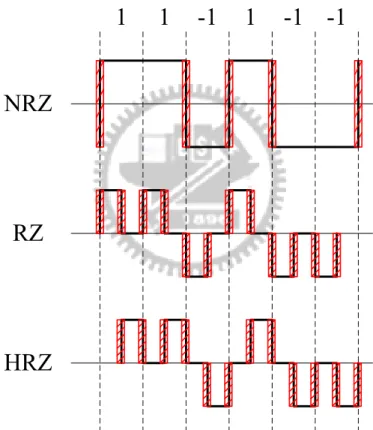
Fig. 3.8 Single-bit NRZ, RZ and HRZ DAC feedback pulse with jitter noise
DAC shapes affect the jitter sensitivity of the CT ΔΣ modulator. This can be illustrated by Fig. 3.8, where single-bit NRZ, RZ and HRZ DAC shapes are shown. The obilque lines indicate that the clock edges are affected by jitter. We can find NRZ DACs are less affected by clock jitter because clock jitter only causes errors
when the output digital code changes. However, for RZ and HRZ DACs, both rising and falling edges of the pulse occur every clock cycle so that they are affected by clock jitter more frequently.
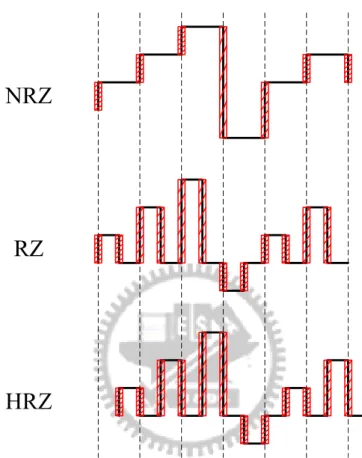
Fig. 3.9 Multi-bit NRZ, RZ and HRZ DAC feedback pulse with jitter noise
We find the jitter noise power can be lowered by reducing the standard deviation of the adjacent modulator output difference. In other words, if the step size of the quantizer is reduced, the jitter noise is lowered. This implies that using multi-bit DACs can reduce the sensitivity to clock jitter. Fig. 3.9 shows multi-bit NRZ, RZ and HRZ DAC feedback pulses with jitter noise. Intuitively NRZ multi-bit DACs should provide best jitter noise immunity than the other two in that its outputs do not need to reset to zero for every clock cycle and hence the average adjacent output difference is smaller [8].
3.2.5 Element Mismatch in a Multi-bit DAC
When we design the CT ΔΣ modulator, the oversampling ratio is usually limited by the circuit speed and power consumption. At the same time, the order and the aggressiveness of the noise shaping are also limited by the stability issue. Therefore, in order to decrease the in-band noise power, an effective way is to use a multi-bit quantizer to reduce the quantization noise in the modulator. Besides, an extra bonus of using multi-bit quantizer is the reduction of the jitter sensitivity.
However, the use of a multi-bit quantizer leads to a multi-bit DAC in the feedback path. The nonlinearity of this DAC severely limits the performance of the modulator. Because the loop filter gain is very high in the signal band, the in-band gain of the S T F is almost equal to one, which means the power of the DAC error will be directly added to the modulator output without much attenuation. So, the linearity of the modulator cannot be higher than that of the DAC.
A very common DAC structure is built from unit elements, in which the nonlinearity of the DAC is mainly caused by the element mismatch. For this DAC structure, an extensively used technique to reduce the DAC error is dynamic element matching (DEM). Using DEM, the bits in the thermometer-code output of the quantizer are rearranged following certain rules by a digital process before they are applied to the DAC. This rearrangement does not affect the data value, but it changes the priority on the selecting of the unit elements in the DAC, which can result in two effects. First, the DAC error becomes uncorrelated with the DAC input, eliminating the signal dependent tones that will appear in the modulator output otherwise. Second, the so-called mismatch shaping will move the error power from low frequencies to high frequencies [2].
In this chapter, the system level and circuit level design of our first work is presented in detail, which includes the determination of the system level parameters, and the system level simulations with non-idealities. After that, the circuit blocks will be discussed, and the modulator is realized with a 0.18 μm CMOS technology and 1.8 V power supply voltage.
4.1 System Level Design
First of all, to design the ΔΣ modulator is determining the most important system level parameters based on the modulator specifications and the semiconductor technology which will be used to realize this modulator. In our first work, the target is to successfully design a CT ΔΣ modulator to reach 68 dB SNDR (signal-to-noise-and-distortion-ratio) within a 1 MHz bandwidth (BW) in a 0.18 μm mixed-signal CMOS process.
However, for a CT ΔΣ modulator, the important specification is the clock jitter sensitivity. It will significantly affect the selection of the system level parameters. We usually assume that the modulator will be evaluated with a clock signal generated by the instrument. Therefore, the jitter value of the clock signal entering
the modulator is determined by the quality of the instrument signal. In our first work, the RMS value of the target jitter tolerance is 20 ps.
The system-level parameters include the oversampling ratio (OSR), the loop filter order (L), the number of the quantizer level (M) and the aggressiveness of the noise shaping which is determined by the maximum out-of-band quantization gain (Qmax) in the MATLAB Control System toolbox. Considering the gain-bandwidth
requirement of the OpAmp with acceptable power consumption and the clock jitter sensitivity, we choose 50 as our OSR value.
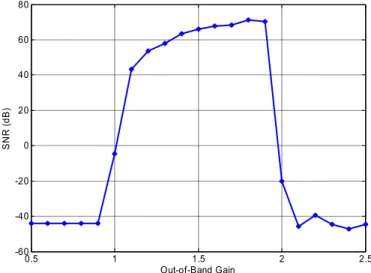
The power consumption of the quantizer increases proportionally to the number of quantization levels. Therefore, for this chip, we determine the number of the quantizer be single. On the other hand, increasing the loop filter order is cheap, but the loop stability issue limits the loop order. Usually, the order should be no more than 5, so we choose 3 as our loop order. Besides, the aggressiveness of the noise shaping is also limited by the stability issue. After MATLAB Control System toolbox simulation, as shown in Fig. 4.1, we choose 1.6 as our out-of-band gain. Based on these requirements, a large amount of simulations were performed by using the MATLAB toolbox to explore the parameter space.
0.5 1 1.5 2 2.5 -60 -40 -20 0 20 40 60 80 Out-of-Band Gain SNR ( d B)
4.2 Architecture of the Loop Filter
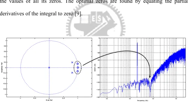
4.2.1 NTF Zero Optimization
When designing wide band ΔΣ modulator, a technique is usually used. That is separating zeros on the unit circle, which means it spreads over the signal range, as shown in Fig. 4.2. By shifting the two zeros from dc (ω = 0) to an optimized value, we can get the 8 dB SQNR improvement. The principle of optimization can be got by the following steps: the normalized noise power, given by the integral of the squared magnitude of the NTF over the signal band, is minimized with respected to the values of all its zeros. The optimal zeros are found by equating the partial derivatives of the integral to zero [9].
Fig. 4.2 Optimal third-order NTF for OSR = 50
In Fig. 4.3, we show the architecture of CT ΔΣ modulator using feedback resistors. The loop filter architecture we use is general feedback structure.
2 S k sT 1 S k sT 3 S k sT 1
DAC DAC2 DAC3
g
Fig. 4.3 The architecture of CT ΔΣ modulator using feedback resistors
4.3 System Level Simulation
As mentioned before, taking the non-idealities into account, we show the output spectrum in this system level simulation of the modulator, which includes all the non-idealities except the thermal noise, as shown in Fig. 4.4. As a comparison, the ideal noise transfer function is also plotted in this figure.
103 104 105 106 107 108 -160 -140 -120 -100 -80 -60 -40 -20 0 SND R ( dB) Frequency (Hz)
4.4 Circuit Level Design
4.4.1 Loop Filter
Fig. 4.5 Simplified block diagram of CT ΔΣ modulator using feedback resistors
The third-order loop filter of our first work design is implemented with CRFB architecture, as shown in Fig. 4.5. The first stage is an active-RC integrator and the following resonators are realized by Gm-C integrators and the resistor. The role of the resonators is to shift the poles of the loop filter to optimum non-zero frequencies in order to reduce in-band quantization noise and get more performance, as mentioned in section 4.2.1.
There are three types of commonly used continuous-time integrators: active-RC integrators, Gm-C integrators and MOSFET-C integrators. In our design, the first stage uses an active-RC integrator rather than Gm-C and MOSFET-C integrators for its superior linearity. Gm-C integrators are chosen for the two resonators to save power. If they were active-RC or MOSFET-C integrators, it would increase the
power consumption considerably because two stage opamps are needed to increase the drive capabilities.
4.4.2 First Stage - Active-RC Integrator
As Fig. 4.6 shown, the current steering DAC feedbacks current to the virtual grounds of the active-RC integrators, therefore good DAC linearity can be achieved. Besides better integrator linearity, this is another advantage compared with using a Gm-C integrator for the first stage. Because the error generated in the first stage could not be shaped to high frequency for ΔΣ modulator, the first stage is especially important. If we use Gm-C integrator as first stage, the DAC would have to connect to the high-swing integrator outputs, and hence DAC linearity would be poor and cause the system performance worse.
The OpAmp in the active-RC integrator uses a folded-cascode topology with a gain enhancement method by adding additional stages to increase DC gain. This method is called gain-boosting [10] [11]. Fig. 4.6 shows the schematic of the gain-boosting folded-cascode OpAmp used in this design. The spice simulation results are shown in Fig. 4.7, including DC gain and phase margin. The detailed specifications are summarized in Table 4.1.
Fig. 4.7 The spice simulation, including DC gain and phase margin Table 4.1 Summary of spice simulation results
Specification Simulation Results
Technology TSMC 0.18μm 1P6M
Unit Gain Frequency 100 MHz ( Cload = 3p )
Phase Margin 85°
DC Gain 87 dB
Out Range 1.6 Vpp
Power Supply 1.8 V
Fig. 4.8 shows the common-mode feedback (CMFB) circuit for the folded-cascode OpAmp. We first assume the two pairs have the same differential voltage, therefore, the current in Q will be equal to the current in 1 Q , while the 3 current in Q will equal the current in 2 Q . This result is valid independent of the 4 nonlinear relationship between a differential pair’s input voltage and its large signal differential drain currents. Now, letting the current in Q be denoted as 2
5 Q 1 Q Q2 Q3 Q4 6 Q / 2 B I + DI IB/ 2- DI B I IB / 2 B I - DI IB/ 2+ DI
Fig. 4.8 Schematic of CMFB circuit
2 / 2
D B
I = I + D , where I IB is the bias current of the differential pair and
I
D is the large signal current change in ID2 , the current in Q is given by 3
3 / 2
D B
I = I - D and the current I Q in is given by 5
5 2 3 / 2 / 2
D D D B B B
I = I + I = I + D I + I - D I = I (4.1)
Thus, as long as the voltage Voutp is equal to the negative value of Voutn, the current through diode-connected Q will not change even when large differential signal 5
voltage are present. Since the voltage across diode-connected Q is used to control 5 the bias voltages of the output stage of the OpAmp, this means that when no common mode voltage is present, the bias currents in the output stage will be the same regardless of whether a signal is present or not.
Next, we consider one thing, what happens when a common mode voltage other than zero is present. We first assume a positive common mode signal is present. This positive voltage will cause the currents in both Q and 2 Q to 3 increase, which causes the current in diode-connected Q to increase, which in 5 turn causes its voltage to increase. This voltage is the bias voltage that sets the current levels in the n-channel current sources at the output of the OpAmp. Thus, both current sources will have larger currents pulling down to the negative rail, which will cause the common mode voltage to decrease, bring the common mode voltage back to zero. By this way, as long as the common mode loop gain is large enough, and the differential signals are not as large as to cause transistors into turn-off, the common mode output voltage will be kept very close to ground [3].
The same method is used for the following two Gm-C integrators to obtain output common-mode voltages since each integrator is followed by a transconductor gain stage with the same architecture.
4.4.3 Following Stage - Gm-C Integrator
VSS VDD VIP M1 M2 VIN M3 M4 M5 M6 M7 M8 M9 M10 M11 M12 Vb1 Vcmfb Vb2 Vb3 Vb3 VON VOP R C CFig. 4.9 Schematic of Gm with source degeneration resistor
With the exception of the first stage integrator, the following two integrators are implemented with Gm-C integrators to save power. A folded-cascode architecture is used with source degeneration resistor, as shown in Fig. 4.9. It achieves the required linearity and it has independent input-output common mode voltages as well. The constant transconductance is shown in Fig. 4.10, it shows the linear range between -0.5V to 0.5V. The spice simulation results are shown in Fig. 4.11, including DC gain and phase margin. The detailed specifications are summarized in Table 4.2.
Fig. 4.11 The spice simulation, including DC gain and phase margin
Table 4.2 Summary of spice simulation results
Specification Simulation Results
Technology TSMC 0.18μm 1P6M
Unit Gain Frequency 16 MHz ( Cload = 3p )
Phase Margin 90°
DC Gain 56 dB
Out Range 1.6 Vpp
Power Supply 1.8 V