國
立
交
通
大
學
電子工程學系 電子研究所
碩 士 論 文
應用於行動照護之
動態取樣全數位心電訊號擷取電路
An All-Digital ADC
with Dynamic Sampling Technique for ECG Acquisition
in Mobile Healthcare Applications
研 究 生:徐佩妤
指導教授:李鎮宜 教授
應用於行動照護之
動態取樣全數位心電訊號擷取電路
An All-Digital ADC
with Dynamic Sampling Technique for ECG Acquisition in
Mobile Healthcare Applications
研 究 生:徐佩妤 Student:Pei-Yu Hsu
指導教授:李鎮宜 Advisor:Prof. Chen-Yi Lee
國 立 交 通 大 學
電子工程學系 電子研究所
碩 士 論 文
A Thesis
Submitted to Department of Electronics Engineering and Institute of Electronics
College of Electrical and Computer Engineering National Chiao Tung University
in partial Fulfillment of the Requirements for the Degree of
Master in
Electronics Engineering
October 2012
Hsinchu, Taiwan, Republic of China
I
應用於行動照護之
動態取樣全數位心電訊號擷取電路
學生:徐佩妤
指導教授:李鎮宜 博士
國立交通大學
電子工程學系 電子研究所
摘要
近年來慢性疾病逐年上升,預防醫學顯得越來越重要。為了可以全天候的監 控人體的生理訊號,並減低人們往來醫院的不便,利用可攜式電子進行全天候的 行動照護成為一個很好的選擇。此研究設計一個應用於行動照護心電訊號擷取電 路之動態取樣全數位類比數位轉換器。以壓控振盪器為主的類比數位轉換器 (VCO-based ADC)可達到高的面積使用效率,以及高的數位整合度,這些都是行 動醫療照護所需要的。此外,隨著製成的微小化,量化於時域的 VCO-based ADC 擁有較好的解析度。此研究設計一有效位數高於 8 位數的 VCO-based ADC 並以 90 奈米製程實現。此 ADC 可支援單一及多個通道的心電訊號擷取電路。 以單一通道應用而言,取樣頻率為 1k 赫茲,此 ADC 可達到 10.48 位數的有 效位數此時的功率消耗為 6.08 瓦特。而在多通道的應用下,此設計可操作在 10k 赫茲底下,以提供 8 個通道的心電訊號擷取。可在維持有效位數為 9.64 位數的 情況下,降低單一通道的功率消耗至 0.62 瓦特。 為了更進一步地降低 ADC 的功率消耗,我們根據生理訊號的特性提出動態 取樣的機制。利用偵測訊號的變化程度,來調整 ADC 的解析度,使得在變化程II
度低的區間 ADC 的功率消耗可大為減少。此機制可在失真率小於 5%的情況下
達到 53% 的功率降低量。與現有的其他機制相比,此方法與有最高的功率降低
III
An All-Digital ADC with Dynamic Sampling
Technique for ECG Acquisition in Mobile
Healthcare Applications
Student: Pei-Yu Hsu Advisor: Chen-Yi Lee
Department of electronics engineering and Institute of electronics,
National Chiao Tung University
Abstract
Heart attack becomes the top cause of death in the U.S. in 2011. The preventive
medicine of the heart disease becomes more and more important. To reduce the effort
for people going to the hospital, the mobile healthcare device is applied to monitor the
electrocardiogram (ECG) signal. Here we design a VCO-based ADC for the ECG
acquisition circuit in mobile healthcare applications. The VCO-based ADC has high
area efficiency and high integration ability with the digital circuit which are suitable
for the mobile device. And also benefits from the technology scaling. Using 90-nm
CMOS process technology, the ENOB of more than 8-bit VCO-based ADC is
implemented. It can support both single channel and multi-channel ECG acquisition
circuit application.
For the single channel, the ENOB of ADC can reach 10.48 bits in sampling
frequency of 1k Hz. The power consumption is 6.08 uW. For the multi-channel
application, our design can operate in sampling frequency of 10k Hz and be turned off
while sampling is finished. In the simulation result, the power of VCO-based ADC is
IV
number of bit.
To reduce the power consumption of our ADC, we apply the dynamic sampling
technique to sense the variation of signal. Then we adjust the resolution of ADC based
on the sensing result. This technique can reduce 53% power of ADC while keeping
distortion less than 5%. Compare with other technique this work has best power
V
致謝
終於,我的碩士生涯告一段落了。在 SI2 的大家庭裡,我學到了許多事情, 不論是課業上、研究上及做人處事上,都讓我成長不少。在這漫長的歲月裡我受 到了許多人的幫助,在此要特別感謝那些幫助我給予我鼓勵的人們。 首先,要感謝我的指導教授 李鎮宜教授。李老師常常提醒我們所做的東西 要從系統的概念下出發,從整個大方向給予我們指導。並且常常叮嚀我們除了研 究之外更要兼顧健康,適時運動放鬆自己,才能有更好的表現。 接著,要感謝 SI2 的學長們。指導我的於爺,常給我許多研究上的幫助及鼓 勵,並且常常包容我的一些小錯誤。新加入的何小杰,在口試前辛苦地幫我看了 投影片,提醒我一些報告時該注意的地方。在電路設計上常給我許多意見的建螢 及昆儒,有點嚴肅講話卻很好笑的宋仔,十分照顧學弟妹擅長當助教的 verilog 達人巴柏,因為有你們的協助,我們碩士研究才可以更加的充實。另外還有其他 430 的學長:阿龍學長、佳龍、長宏、義澤、欣儒、人偉,十分感謝你們給予我 的鼓勵及意見。 另外還有一群一起奮鬥的夥伴們:經常互相鼓勵互相安慰的皮皮,常提供我 很好的情緒抒發管道,並且一起在互相鞭策下成長。常給我很多各方面意見的美 維,讓我可以從更多元的觀點思考問題。隨敲隨應的囧君,有什麼問題都不怕找 不到人。陪我說說笑笑的雞皮,讓我的緊繃的生活可以得到放鬆。我的合作夥伴 博堯,常常可以互相照應一起實施早起計畫。實驗室的奇葩恕平,常常帶動實驗 室活潑的氣氛。以及許多其他給予我鼓勵的朋友們,因為有你們的陪伴,讓我的 碩士生涯更加的愉快更有前進的動力。 最後,我要感謝我的家人們,在我的求學階段給予我許多的支持與鼓勵,讓 我可以順利的完成求學的生涯。當我遇到瓶頸時可以有個傾訴的管道,並且站在 長輩的立場給我適當的建議。謝謝你們總給予我滿滿的信心,讓我可以更加的相 信自己,並且總是在我身邊陪著我讓我可以毫無顧忌地向前衝。VI
Table of Contents
Chapter 1: Introduction ... 1
1-1 Motivation ... 1
1-2 ECG acquisition circuit ... 2
1-2.1 ECG signal characteristic ... 2
1-2.2 ECG acquisition circuit block ... 3
1-2.3 Design Consideration ... 5
Chapter 2: Theory... ... 7
2-1 ADC Performance Item ... 7
2-1.1 DC accuracy ... 7
2-1.2 Dynamic performance ... 8
2-2 VCO-based ADC ... 11
2-2.1 Architecture... 12
2-2.2 Sample and hold action ... 15
2-2.3 First-order noise shaping... 16
2-2.4 SNR ... 17
2-2.5 Non-ideal effects ... 19
2-3 VCOs ... 24
2-3.1 Ring oscillator basics ... 25
2-3.2 Jitter... 27
Chapter 3: Proposed VCO-based differential input ADC ... 29
3-1 Brief Architecture ... 29
3-2 VCO Design ... 30
VII
3-2.2 Supply controlled delay cell ... 38
3-2.3 Bulk controlled delay cell ... 42
3-2.4 Ground controlled delay cell ... 47
3-2.5 Choice of VCO topology ... 52
3-3 Counter ... 53
3-3.1 Synchronous ... 54
3-3.2 Asynchronous ... 54
3-3.3 Performance comparison ... 57
3-4 Sampling Flip-Flop... 57
3-4.1 Standard cell flip-flop ... 58
3-4.2 Gated flip-flop ... 60
3-4.3 Power comparison ... 61
3-5 Flip-flops metastability compensation circuit ... 62
Chapter 4: Simulation Results………. ... 63
4-1 INL and DNL ... 63
4-2 Waveform ... 64
4-3 FFT result ... 65
4-4 Performance Summary ... 65
Chapter 5: Dynamic Sampling Technique…………. ... 69
5-1 Dynamic sampling principle ... 70
5-1.1 Information estimation ... 70
5-1.2 Sampling Control for power reduction ... 73
5-2 Performance Item ... 74
5-2.1 Percentage Reduction Distortion (PRD) ... 74
VIII
5-2.3 Percentage Power Reduction (PPR)... 75
5-3 Architecture ... 75
5-3.1 Partial dynamic sampling (PDS) technique: low distortion mode ... 76
5-3.2 Partial dynamic sampling (PDS) technique: data compression mode78 5-3.3 Fixed dynamic sampling (FDS) technique ... 80
5-3.4 Various dynamic sampling (VDS) technique ... 82
5-3.5 Performance summary and comparison ... 84
5-4 Circuit simulation ... 84
5-4.1 ECG Waveform ... 85
5-4.2 Noise Influence ... 85
5-5 PRD &Power reduction result ... 86
5-6 Chip Implementation ... 87
Chapter 6: Conclusion and Future work ... 89
6-1 Conclusion ... 89
6-2 Future work ... 90
IX
List of Figures
Fig. 1-1 Nature of ECG signal ... 2
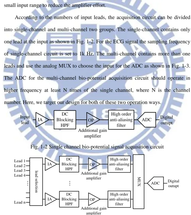
Fig. 1-2 Single channel bio-potential signal acquisition circuit ... 4
Fig. 1-3 Bio-potential signal acquisition circuit ... 4
Fig. 2-1 FFT result of ADC output code ... 9
Fig. 2-2 Illustration of SFDR ... 11
Fig. 2-3 (a) Conventional ADC (b) VCO-based ADC ... 12
Fig. 2-4 Single phase VCO-based ADC ... 13
Fig. 2-5 Timing diagram of single-phase VCO-based ADC ... 13
Fig. 2-6 Multi-phase VCO-based ADC ... 14
Fig. 2-7 Timing diagram of multi-phase VCO-based ADC ... 15
Fig. 2-8 Operation principle of VCO phase quantization ... 17
Fig. 2-9 Illustration of jitter definition timing diagram ... 20
Fig. 2-10 VCO phase noise; (a) phase noise model (b) illustration of phase noise ... 21
Fig. 2-11 Illustration of timing item definition ... 23
Fig. 2-12 Definition of metastability window ... 24
Fig. 2-13 Ring oscillators: (a) single-end oscillator (b) differential oscillator (odd stage) (c) differential oscillator (even stage with inverted net) ... 25
Fig. 3-1 VCO-based ADC architecture ... 30
Fig. 3-2 Invertor based ring oscillator ... 31
Fig. 3-3 MOSFET switching circuit with capacitance ... 31
Fig. 3-4 Simple digital MOSFET model ... 31
Fig. 3-5 Schematic of current controlled delay cell ... 34
X
Fig. 3-7 Overall VCO schematic ... 35
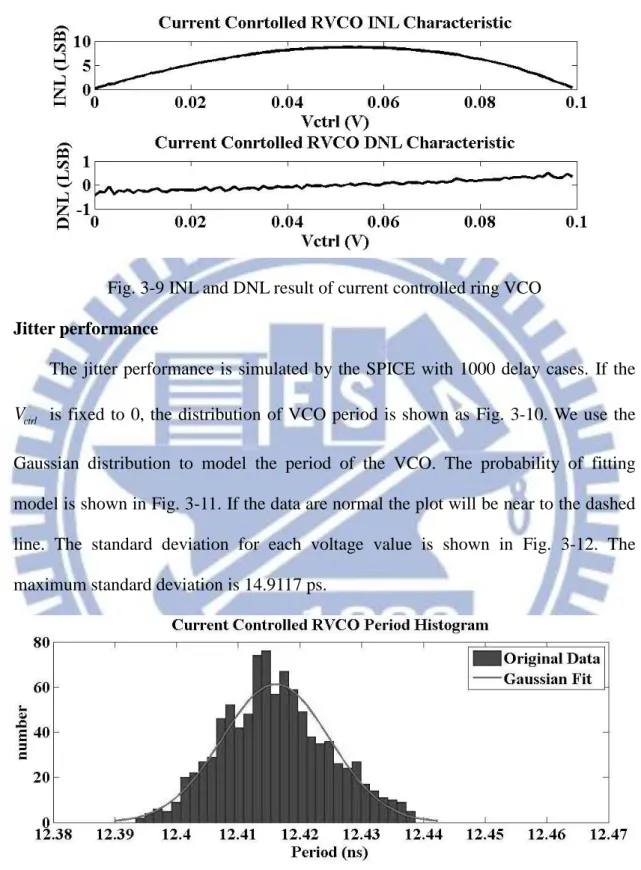
Fig. 3-8 Frequency characteristic of current controlled ring VCO... 35
Fig. 3-9 INL and DNL result of current controlled ring VCO ... 36
Fig. 3-10 Distribution of period of current controlled ring VCO ... 36
Fig. 3-11 Probability plot of current controlled ring VCO ... 37
Fig. 3-12 Standard deviation of the period of current controlled ring VCO ... 37
Fig. 3-13 Power consumption of current controlled VCO ... 38
Fig. 3-14 Schematic of supply controlled delay cell ... 39
Fig. 3-15 Delay characteristic of supply controlled delay cell ... 39
Fig. 3-16 Frequency characteristic of supply controlled ring VCO ... 40
Fig. 3-17 INL and DNL characteristic of supply controlled ring VCO ... 40
Fig. 3-18 Distribution of Period of supply controlled ring VCO ... 41
Fig. 3-19 Gaussian probability plot of supply controlled ring VCO ... 41
Fig. 3-20 Standard deviation of period of supply controlled ring VCO ... 42
Fig. 3-21 Power consumption of supply controlled ring VCO... 42
Fig. 3-22 Schematic of bulk controlled delay cell ... 44
Fig. 3-23 Delay characteristic of bulk controlled delay cell ... 44
Fig. 3-24 Frequency characteristic of bulk controlled ring VCO ... 45
Fig. 3-25 INL and DNL result of bulk controlled ring VCO ... 45
Fig. 3-26 Distribution of period data and the Gaussian fitting line ... 46
Fig. 3-27 Gaussian distribution probability plot... 46
Fig. 3-28 Standard deviation of period of bulk controlled ring VCO ... 47
Fig. 3-29 Power consumption of bulk controlled ring VCO ... 47
Fig. 3-30 Schematic of ground controlled delay cell ... 49
XI
Fig. 3-32 Frequency characteristic of ground controlled ring VCO... 50
Fig. 3-33 INL and DNL of ground controlled ring VCO ... 50
Fig. 3-34 Distribution of period of ground controlled ring VCO ... 51
Fig. 3-35 Probability plot of Gaussian fitting model ... 51
Fig. 3-36 Standard deviation of period of ground controlled ring VCO ... 52
Fig. 3-37 Power consumption of ground controlled ring VCO ... 52
Fig.3-38 synchronous counter: (a) Architecture; (b) Timing diagram ... 54
Fig.3-39 Asynchronous counter: (a) Architecture; (b) Timing diagram ... 55
Fig.3-40Timing diagram for asynchronous sampling ... 57
Fig.3-41 Power trend of synchronous and asynchronous counter ... 57
Fig. 3-42 flip flop testing circuit ... 59
Fig. 3-43 Simulation results of timing items of low power flip flop cells. The metastability due to the minimal data-to-output delay is 0.151 ns. ... 60
Fig.3-44 Power consumption of flip-flops ... 60
Fig.3-45 Gated flip-flop: (a) Gated flip-flop circuit; (b) En window circuit... 61
Fig.3-46 Power of gated flip-flop ... 61
Fig. 4-1 DNL of ADC ... 63
Fig. 4-2 INL of ADC ... 64
Fig. 4-3 ADC output of 1k Hz sampling rate ... 64
Fig. 4-4 ADC output of 10k Hz sampling rate ... 65
Fig. 4-5 Power Spectral Density of ADC output in 1k Hz sampling frequency ... 65
Fig. 4-6 Power Spectral Density of ADC output in 10k Hz sampling frequency ... 65
Fig. 4-7 Power distribution ... 68
Fig. 5-1 ECG signal ... 69
XII
Fig. 5-3 Brief illustration of partial ADC-SP cycle estimation ... 71
Fig. 5-4 Brief illustration of fixed DS CLK estimation ... 72
Fig. 5-5 Brief illustration of various DS frequency estimation ... 72
Fig. 5-6 illustration of PDS-low distortion mode technique ... 77
Fig. 5-7 PRD vs. Power consumption of PDS high resolution mode... 78
Fig. 5-8 illustration of PDS-data compression mode technique ... 79
Fig. 5-9 PRD vs. Power consumption of PDS data compression mode ... 79
Fig. 5-10 illustration of FDS technique ... 81
Fig. 5-11 PRD vs. Power consumption of FDS ... 81
Fig. 5-12 illustration of VDS technique ... 83
Fig. 5-13 PRD vs. Power consumption of VDS ... 83
Fig. 5-14 ECG signal simulation result ... 85
Fig. 5-15 PLI noise influence ... 86
Fig. 5-16 AWGN noise influence ... 86
Fig. 5-17 PRD vs. Power consumption ... 87
XIII
List of Tables
Table 1-1SPECIFICATION (IEC 60601-2-47 [3]) ... 5
Table 3-1 Performance comparison of VCO ... 53
Table 3-2 Power comparison of standard cell flip-flops ... 59
Table 3-3 Delay time in each corner ... 62
Table 4-1 Comparison Table ... 67
Table 4-2 Details power consumption of each block ... 68
1
Chapter 1:
Introduction
1-1
Motivation
Heart attack becomes the top cause of death in the U.S. in 2011. The preventive
medicine of the heart disease becomes more and more important. To reduce the effort
for people going to the hospital, the mobile healthcare devices are applied to monitor
the electrocardiogram (ECG) signal. In the mobile healthcare system, it contains the
acquisition circuit and the digital processor. The analog-to-digital converters (ADCs)
are interfaced between the analog and digital domain which play the important role on
influencing the performance of systems. The conventional ADCs quantize the voltage
information in analog domain. However, as the technology scales, the supply voltages
become lower. Therefore, the threshold voltage becomes relative high and results in
the difficulty of converting signal in analog domain. And also for the reduction of
voltage headroom for signal swing, the signal amplitude is reduced. With the same
noise floor, the Signal-to-Noise ratio (SNR) becomes worse.
In contrast, the resolution in time domain is enhanced in the advanced CMOS process. It’s better to deal with the signal in time domain rather than voltage domain. The Voltage-Controlled-Oscillator (VCO) based ADCs convert the voltage into the
time domain take this advantage. The frequency of time-based signal is modulated by
the input voltage, and the information is quantized and processed by the digital logic.
2
voltage domain which is attractive for the low voltage advanced CMOS process.
Another benefit for this type of ADC is that it is mostly composed by the digital
blocks which can be compatible to the digital design flow and can be easily integrated
with the digital system.
1-2
ECG acquisition circuit
1-2.1 ECG signal characteristic
Before we introduce the ECG acquisition circuit, we should understand the
characteristic of ECG signal. The Electrocardiogram (ECG) signal is composed of
three components: the common-mode signal, differential electrode offset and actual
ECG signal as shown in Fig. 1-1.
0V Common-Mode 50Hz ~ 60Hz ±300mV Electrode Offset ±3mV 0.05Hz ~150Hz ±3mV 0.05Hz ~150Hz ECG Signal ECG Signal
Fig. 1-1 Nature of ECG signal
Common-mode signal are the interferences of 50/60Hz power line coupling,
motion artifacts, radio from other electronic equipment, etc. It can be reduced by
increasing the isolation of ground of front-end and the ground of earth, or increasing
the common mode rejection ratio (CMRR) of the front-end circuit by feeding the
signal to cancel the common mode interference by mixed signal feedback loop [1], or
driving the body with a common mode feedback (e.g. drive right leg (DRL) circuits
3
electrode-skin interface, which is approximately up to 300mV and the front-end
circuits should be made sure that the offset will not cause the saturation of acquisition
circuit. It can be reduced by adding AC coupling capacitor, the high pass filter, or the
servo feedback. The actual ECG signal appears in each lead is limited to ±6mV in
differential amplitude and 0.05Hz to 150Hz in frequency.
1-2.2 ECG acquisition circuit block
Conventionally, an ECG acquisition circuit is consisted of an instrumentation
amplifier (IA), a programmable gain amplifier (PGA), an antialiasing filter and an
analog to digital convertor (ADC).
The instrumentation amplifier which has high common-mode rejection ratio
(CMRR) and high input impedance is used as the input stage with a relative low gain
to avoid the saturation due to the DC offset. Based on the resolution of ADC, there are
two different approaches to process the signal [2]. The first one uses the high gain
amplifier to amplify the signal significantly and uses a low resolution ADC to convert
the amplified signal into digital value. In this kind of system, total gain is increased by
adding the additional PGA as the main amplifier stage. The noise performance of this
stage should be considered carefully to make sure that it will not dominate the total
noise of system. Between the input instrumentation amplifier and the PGA, the high
pass filter (HPF) should be added to remove the amplified DC offset. After the gain
stage, the antialiasing filter is used before signal fed into the convertor. For the
Nyquist rate convertor the antialiasing filter should be very sharp to avoid the aliasing
noise. [2]
The other way is to use the low gain amplifier and the high resolution ADC to
4
removed. Only the low gain instrumentation amplifier is used to amplify the input
signal. It makes the amplified noise is less than the traditional architecture, and also
DC offset will not be amplified by the high gain amplifier that will not cause the
saturation issue. The DC variation can be filtered in the digital domain after converted,
so the DC block high pass filter can be eliminated. The active antialiasing filter can
also be replaced by the simple RC filter. In this thesis, we design an ADC with low
small input range to reduce the amplifier effort.
According to the numbers of input leads, the acquisition circuit can be divided
into single-channel and multi-channel two groups. The single-channel contains only
one lead at the input as shown in Fig. 1-2. For the ECG signal the sampling frequency
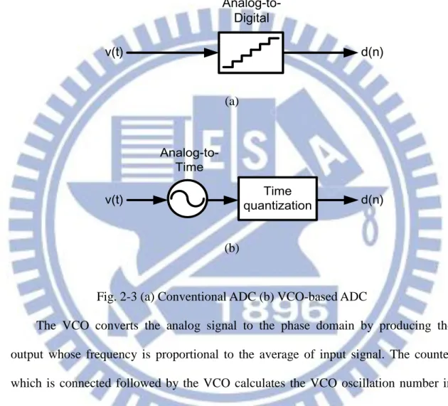
of single-channel circuit is set to 1k Hz. The multi-channel contains more than one
leads and use the analog MUX to choose the input for the ADC as shown in Fig. 1-3.
The ADC for the multi-channel bio-potential acquisition circuit should operate in
higher frequency at least N times of the single channel, where N is the channel
number. Here, we target our design for both of these two operation ways.
IA DC Blocking HPF Additional gain amplifier High order anti-aliasing filter ADC Input lead Digital outupt OP
Fig. 1-2 Single channel bio-potential signal acquisition circuit
ADC Lead 1 Digital outupt IA DC Blocking HPF Additional gain amplifier High order anti-aliasing filter OP IA DC Blocking HPF Additional gain amplifier High order anti-aliasing filter OP le ad s el ec tio n M U X … Lead 2 Lead 3 Lead 4 Lead n …
5
1-2.3 Design Consideration
The design considerations for the ECG signal acquisition circuit is given in IEC
60601-2-47 medical electrical instrument standard [3]. First, the input signal is limited
to ±6mV in differential amplitude. To get the information of such small amplitude, the
resolution of system should more than 50uV/LSB. To achieve this requirement the
resolution for ADC should be more than 6.9 bits. Here we design an ADC in 8 bits.
The Bandwidth of the acquisition circuit should cover 0.05-150Hz. Second, the design
should cover the temperature of 0~45°C. Third, the influence of DC offset and
variation should be reduced to ±10%. Forth, the input refer noise of acquisition circuit should less than 50μVrms. Fifth, because of the high impedance of ECG electrodes, the input impedance of acquisition circuit should have high input impedance more
than 10 MΩ. The last one is the circuit should have high CMRR which is more than
60dB to reduce the common mode interference. For single-channel application and
multi-channel application the sampling frequency is 1k Hz and 10k Hz respectively.
The design specification is summarized as follow:
Item Specification
Input characteristic Amplitude: ±6mVpp-diff Bandwidth: 0.05-150Hz
DC offset: ±300mV (variation <±10%)
Sampling Frequency 1kHz (single-channel)/ 10k Hz (multi-channel)
Resolution >50uV/LSB (8 bits)
Temperature 0-45°C
Input impedance @ 10MHz >10 Mohms
CMRR >60 dB
Input refer noise <50 uVrms
Table 1-1SPECIFICATION (IEC 60601-2-47 [3])
6
the input stage. For the ADC we only consider the bandwidth of input, the input range
7
Chapter 2:
Theory
2-1
ADC Performance Item
Before we introduce the basic concept of VCO-based ADCs, we will first give
some common performance items of ADC. The ADC performance items can
generally be separated into two groups: dc accuracy and dynamic performance. For
different application, the designer will focus on different type of performance item.
For example, for the application which should deal with specific frequency should
pay more attention on dynamic performance. For the applications that process
dc-like input signal or the measured voltage is relative to some physical
measurement, like temperature sensor, should care more about the dc accuracy. For
our application, the ADC will sense the ECG signal whose accuracy should be
considered and for specific input frequency of ECG signal, the dynamic performance
should also be cared about. Here, we list some common items that we focus on.
2-1.1 DC accuracy
DC accuracy can be calculated by sending the sweep voltage as input to get the
transfer function of ADCs. Based on the transfer function of ADCs we can define
several performance items to estimate the characteristic of ADCs. Here we list two
8 Differential Nonlinearity (DNL)
For the ideal ADCs, the voltage difference between each transition should be
equal to one Least Significant Bit (LSB). Here, the LSB of ADC means the step size
of smallest level that ADC can convert as shown as follow:
2N
VFS
LSB (2.1)
where the VFS stands for full scale input and N represent the resolution of ADC. For
the N-bit quantizer, it will have 2N levels.The difference of the voltage transition space between one code to the next is call the differential nonlinearity (DNL) which
can be calculated as below:
n 1
V
DNL
n1
LSBV
V
(2.2)Integral nonlinearity (INL)
The integral nonlinearity (INL) is the deviation of the code from the ideal
transfer function. For simplifying the calculation, the ideal transfer function here we
defined is the line that directly connects the “zero” and “full scale” of the ADC
transfer instead of the best-fit line. The INL is determined by measuring the voltage at
code transitions and comparing them to the ideal voltage. Here should be noticed that,
the nonlinearity of ADC will cause the distortion. The INL will affect the dynamic
performance of ADCs.
2-1.2 Dynamic performance
The other part is about dynamic performance. It is measured by sending a single
tone frequency sine wave at input and performing the Fast Fourier Transform (FFT)
on the output code of ADC. These types of performance estimate the noise
9
frequency is the input frequency. Others are regarded as noise and characterized with
respect to the desired signal.
Fig. 2-1 FFT result of ADC output code
Signal-to-Noise Ratio (SNR)
The signal to noise ratio (SNR) is the ratio of power of fundamental signal to the
power of noise floor, excluding the DC signal and the spur power as shown in
equation(2.3). It is usually expressed in decibels (dB).
si ( ) ( )
(
) 20log
gnal rms noise rmsV
SNR dB
V
(2.3)The noise power in SNR calculation doesn’t include the harmonic distortion,
only the quantization noise is considered. For the ideal ADC with given resolution N
bits, the theoretical best SNR is as bellow:
(
) 6.02
1.76
SNR dB
N
(2.4)Signal-to-Noise and Distortion Ratio (SiNAD also called SNDR)
For the SNR, the noise power doesn’t contain the harmonic distortion power. For
the SiNAD (SNDR), it gives more complete information about the noise behavior.
10
and the harmonic distortion power as shown below:
2 2 2 2 2 2 3 420log
...
sig n noiseV
V
V
SiNAD SN
V
DR
V
V
(2.5)where V2is the amplitude of the second harmonic, V3is the amplitude of third harmonic and so on. The other way to calculate the SiNAD (SNDR) is performed in
time domain. First, record the output data of ADC and fit the sine wave to the data at
the sending frequency. Then the rms noise can be calculated by 2 2 1 1 ( ) M n n n rms noise y y M
(2.6) where ny : output data of ADC
n
y: best-fit sine wave
M: number of record data
The SiNAD (SNDR) can be calculated by equation(2.7)
rms signa
SiNAD SND
l
rms
R
noise
(2.7)Where rms signal is equal to sine wave peak/
2
.Spurious-Free Dynamic Range (SFDR)
Spurious-Free Dynamic Range (SFDR) is the magnitude difference between
signal and the highest spur peak as shown in Fig. 2-2. Most of highest spur occurs on
11
Fig. 2-2 Illustration of SFDR
Effective number of bits (ENOB)
Effective number of bits (ENOB) is the one of the method comparing the rms
noise of ADC to the quantization noise of the ideal ADC which has that amount of
bits of resolution. For example, if a real 8-bit ADC has ENOB of 7; the rms noise it
produces is equal to the one ideal 7-bit ADC produces. There are two common
methods to calculate the ENOB. The first one is converted from SNDR by
equation(2.8). This formula is similar to the relation between the SNR and ADC
resolution in equation(2.4).
1.76( ) 6.02
SNDR dB
ENOB (2.8)
The second one is to be calculated in the time domain as shown in equation(2.9),
where the rms noise is calculated by equation(2.6).
2 2 log ( ) log ( ) 12 rms noise ENOB N
ideal rms quantization error full scale range
rms noise (2.9)
2-2
VCO-based ADC
Here we introduce some basic concept of VCO-based ADC and some non-ideal
12
2-2.1 Architecture
The conventional ADCs are built using analog circuit and quantize the input in
voltage domain directly. For the VCO-based ADCs, they convert the analog input into
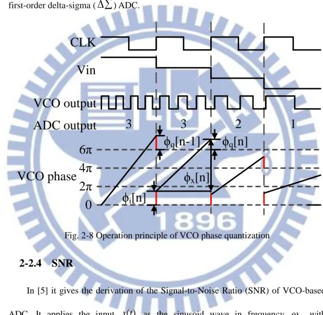
time information that quantized by the digital circuit as shown in Fig. 2-3.
Analog-to-Digital v(t) d(n) (a) Time quantization v(t) d(n) Analog-to-Time (b)
Fig. 2-3 (a) Conventional ADC (b) VCO-based ADC
The VCO converts the analog signal to the phase domain by producing the
output whose frequency is proportional to the average of input signal. The counter
which is connected followed by the VCO calculates the VCO oscillation number in
the given sampling period.
For the single phase VCO-based ADC, the architecture is shown as Fig. 2-4. It
applies only single counter to sense the transition of 1-phase VCO. The timing
diagram of this architecture is shown as Fig. 2-5.The counter value is read out at the
end of very cycle can be seen as the ADC output which has the relation with the
analog input as equation(2.10). After value of counter is read, the counter is reset to
13 Counter Vin EN CLK Sampling Flip-Flops OUT Single-phase VCO
Fig. 2-4 Single phase VCO-based ADC
Vin
VCO output
Counter output
ADC output
CLK
1 2 1 2 3 4 1 2 3 1 2 14
3
2
1
2
Fig. 2-5 Timing diagram of single-phase VCO-based ADC
( ) , ( ) ( ) s VCO vco s
Time for VCO oscillation number calculation ADC digital output D n
VCO oscillation period P
usually the counter counts whole sampling period P t F t F (2.10) s vco s vco
where P : Period of sampling CLK
P : Period of VCO which is modulated by the analog input F : Frequency of sampling CLK
F : Frequency of VCO which is modulated by the analog input
For the single-phase VCO-based ADC the resolution of ADC is depended on the
relation between the sampling frequency and the frequency range of VCO as shown
14
log2 max( ) min( )
log2 min( ) max( ) ( ) max( ) min( ) log2 vco vco vco vco s
ADC resolution B ceil D D
Time for VCO oscillation Time for VCO oscillation ceil
P P
usually the osillation cover whole sampling period F F ceil F F _ log2 s vco range s F ceil F (2.11)
The other type of architecture is the multi-phase VCO-based ADC. Counters are
applied to more than one phase of VCO as shown in Fig. 2-6, 3-phase VCO-based
ADC for example. The ADC output is got by adding the counter value for each phase.
In this type of VCO-based ADC, for the N-phase VCO, the resolution can be N times
than the single phase one. The timing diagram of the 3-phase VCO-based ADC is
shown in Fig. 2-7. However, the power and the complexity of multi-phase VCO-based
ADC increase, so for our design, we choose the single-phase VCO-based ADC.
Counter Vin EN CLK Sampling Flip-Flops Multi-phase VCO Counter Sampling Flip-Flops Counter Sampling Flip-Flops
OUT
+
15
Vin
VCO
outputs
Counter
outputs
ADC output
CLK
1 2 1 2 3 4 1 2 3 1 2 112
9
6
3
6
1 2 1 2 3 4 1 2 3 1 2 1 1 2 1 2 3 4 1 2 3 1 2 1Fig. 2-7 Timing diagram of multi-phase VCO-based ADC
2-2.2 Sample and hold action
Usually, the sample and hold circuit is required when the input voltage is in high
frequency relative to the operation of A/D process. In [4], it gives the analysis for the
omitting of the sample and hold circuit. We consider the sine wave input as
( ) sin(2 )
IN IN
V t A
f t (2.12)Where A is the amplitude and fIN is the input frequency. We set TC as the maximum conversion time of the voltage control delay cell which is the largest time
difference between the input and output digital edge for any input. The input voltage
cannot change more than VLSB within TC. This set the upper bound for input voltage slope
2
IN LSB IN CdV
V
slope
Af
dt
T
(2.13) Where16 2 2 1 LSB D A V (2.14)
D is the resolution of ADC. Combine and rearrange the equation(2.13) and
equation(2.14)
1
(2
1)
IN D Cf
T
(2.15)If the input frequency and the conversion time satisfy the condition in
equation(2.15), the ADC without sample and hold circuit can even achieve the
resolution D as the same as the one with sample and hold circuit.
2-2.3 First-order noise shaping
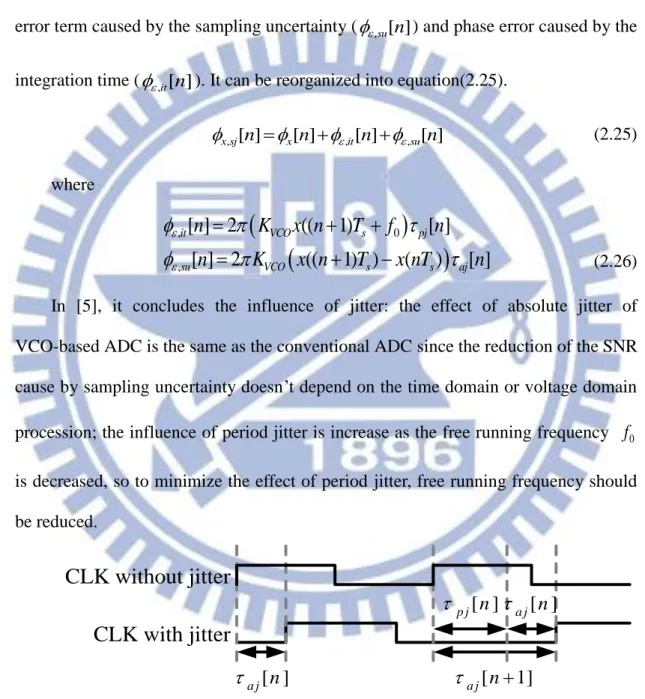
The counter for VCO-based ADC can be seen as the phase quantizer. It quantizes
the phase by counting rising or falling edge during sampling period. The step of
quantization is 2 for single edge trigger. For both rising and falling edge trigger the quantization step is
. For the multi-phase VCO-based ADC with N phases, the quantization step is 2 / N for single edge trigger and / N for double edge trigger.The phase residue of quantization error will be passed to the next sampling as the
initial phase as shown in Fig. 2-8. We set q[ ]n as the quantization error in nth sample which will be equal to the initial phase of (n+1)th sample
i[n1] and[ ]
x n
as the VCO phase change due to the analog input in nth sample. The output of VCO quantizer can be represented as[ ]
( [ ]
[ ]
[ ])
2
( [ ]
[
1]
[ ])
2
x i q x q qN
y n
n
n
n
N
n
n
n
(2.16)17
The result of taking the z-transform of equation(2.16) is shown as below:
1
( ) ( ) ( 1) ( ) 2 x q N Y z z z z
(2.17)We can see that the quantization error term is first-order shaped, hence, it can be
said that the VCO-based ADC has the same performance compared with the
first-order delta-sigma (
) ADC.Vin
VCO output
ADC output
CLK
VCO phase
3
3
2
1
0
2π
4π
6π
ϕ
q[n-1]
ϕ
i[n]
ϕ
q[n]
ϕ
x[n]
Fig. 2-8 Operation principle of VCO phase quantization
2-2.4 SNR
In [5] it gives the derivation of the Signal-to-Noise Ratio (SNR) of VCO-based
ADC. It applies the input
x t
( )
as the sinusoid wave in frequency
in with amplitude A as equation(2.18).( ) cos( in )
x t A
t (2.18)18
0 ( 1) 0 ( 1) 0 0 [ ] 2 ( ( ) ) 2 ( cos( ) ) 2 (2 1) 2cos sin 2 2 (2 1) 2 sinc cos 2 nTs x VCO n Ts nTs VCO in n Ts VCO in in in in VCO in A n K x t f dt K A t f dt K A Ts n Ts f Ts Ts n K ATs f Ts f Ts
(2.19)where Ts is the sampling period, f0 is the free-running frequency of VCO and
VCO
K is the gain of VCO. The power of signal in phase domain is
2
1 2
x
P A (2.20)
And for the N phase VCO-based ADC the power of quantization noise which is
derived in [6] is shown as follows:
2 2 3 1 2 1 12 3 n P N OSR
(2.21) Where(
)
2
s inf
OSR Over Sampling Ratio
f
, fsrepresents the sampling frequencyand fin represents the input frequency. Finally, the SNR can be calculated by
1 6.02 3.41 30log 20log sinc( )
2 x n P SNR P M OSR OSR (2.22)
where M is the resolution of ADC as shown in equation(2.23) for N phases
VCO-based ADC. 2
log (
range)
sf
N
M
f
(2.23)19
from the traditional delta-sigma modulator. For the VCO-based ADC, M is inversely
proportional to the sampling rate while for the delta-sigma ADC M is proportional to
the sampling rate. Another phenomenon should be noted is the low pass filter
characteristic of the VCO-based ADC. The average nature of VCO and the absence of
the S/H causes the last term of the equation(2.22) which is the sinc-shaped function
that filter out the integer multiples of the sampling frequency. This phenomenon
causes the reduction of SNR as input frequency increase. When VCO-based ADC is
operated in the Nyquist rate, the SNR is reduced by 3 dB and the signal near the
integer multiples of the sampling frequency is filtered out.
2-2.5 Non-ideal effects
In the real world there are some non-idealities need to be considered, such as
jitter, nonlinearity, mismatch, metastability. These non-ideal effects reduce the
performance of the VCO-based ADC. Here, we take these effects into consideration
and give the analysis of the influence. These analyses can be referred to [5].
Jitter of sampling CLK
The sampling CLK for VCO-based ADC is not only used for sampling data as
other types of ADC but also applying the reference time for integrating the phase of
VCO. The effects of jitter of sampling CLK can be separated into two groups: the
sampling uncertainty due to the vibration of the rising edge and the integration error
caused by the unequal period. The former one is influenced by the absolute jitter
[ ]
aj n
which is defined as the time difference between the nthedge of the ideal and the practical CLK. The later one is affected by the period jitter pj[ ]n which is defined as the time difference between nthperiod of the ideal and the practical CLK
20 equation(2.24). ( 1) [ 1] , 0 ( ) [ ] [ ] 2 ( ( ) ) s aj s aj n T n x sj VCO n T n n K x t f dt
(2.24)This equation can be separated into the original phase information (
x[ ]n ) phase error term caused by the sampling uncertainty (,su[ ]n ) and phase error caused by theintegration time (,it[ ]n ). It can be reorganized into equation(2.25).
, [ ] [ ] , [ ] , [ ] x sj n x n it n su n (2.25) where
, 0 ,[ ] 2
((
1)
[ ]
[ ] 2
((
1) )
(
)
[ ]
it VCO s pj su VCO s s ajn
K
x n
T
f
n
n
K
x n
T
x nT
n
(2.26)In [5], it concludes the influence of jitter: the effect of absolute jitter of
VCO-based ADC is the same as the conventional ADC since the reduction of the SNR
cause by sampling uncertainty doesn’t depend on the time domain or voltage domain
procession; the influence of period jitter is increase as the free running frequency f0
is decreased, so to minimize the effect of period jitter, free running frequency should
be reduced.
CLK without jitter
CLK with jitter
[ ] a j n
a j[n1] [ ] p j n
a j[ ]nFig. 2-9 Illustration of jitter definition timing diagram
VCO phase noise
21
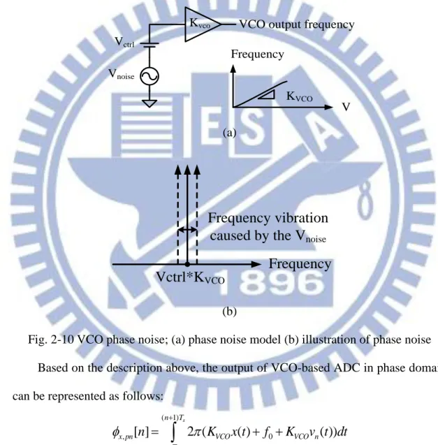
applied at the input and is converted into the frequency through the gain of VCO. As
shown in Fig. 2-10, for a given constant voltagevctrl, the output frequency of the VCO with conversion gain,KVCO should be the constant value, KVCO ctrlV . But if there is a noise source at input, the output frequency will vary in a certain interval. This
phenomenon in frequency domain can be characterized in phase noise performance.
V Frequency KVCO Kvco Vctrl Vnoise
VCO output frequency
(a)
Frequency vibration
caused by the V
noiseVctrl*K
VCOFrequency
(b)
Fig. 2-10 VCO phase noise; (a) phase noise model (b) illustration of phase noise
Based on the description above, the output of VCO-based ADC in phase domain
can be represented as follows:
( 1) , 0 ( 1) [ ] 2 ( ( ) ( )) [ ] 2 ( ) [ ] (( 1) ) ( ) s s s s n T x pn VCO VCO n nT n T x VCO n nT x pn s pn s n K x t f K v t dt n K v t dt n n T nT
(2.27)22
where ( ) : :
n
pn
v t input refer noise of theVCO output phase noise of theVCO
Taking z-transform of equation (2.27), we can get the result as below:
, ( ) ( ) ( 1) ( )
x pn z x z z pn z
(2.28)
It shows that the phase noise of VCO-based ADC is first-order shaped. [5] We
further derive the SNR influenced by the VCO phase noise which is shown in
equation(2.29). It assumes the VCO has phase noise Ł [dBc/Hz] at the frequency
offset, foffset and fin is denoted as the frequency of input signal.
2 210log(
)
16
VCO vpn offset inK
A
SNR
Łf
f
(2.29)VCO tuning characteristic nonlinearity
The VCO is the key component to convert the analog domain voltage signal into
the frequency or phase information. Nonlinearity of VCO tuning characteristic
directly influences the linearity of the digital code of the VCO-based ADC. It causes
the harmonic spurs occur at the ADC output spectrum and reduces the SNDR of ADC.
We expand the VCO gain as the high order polynomial and the phase caused by the
nonlinearity of VCO can be represented as follows:
2 3 , 2 3 ( 1) [ ] 2 ( ( ) ( ) ( ) ) ( ) cos( ) nTs x nl fr VCO n Ts in n f K x t a x t a x t dt where x t A t
(2.30)[5] shows the power of second and third harmonic spurs as below:
2 2 2 2 2 2 2
(2 )
1
2
sinc
2
2
in in s sf
P
a A
f
f
(2.31)23 2 2 3 2 3 2 3
(2 )
1
3
sinc
2
4
in in s sf
P
a A
f
f
(2.32)We can see that the nth harmonic spur is filtered by sinc function which has the
nulls at the integrate multiples of fs. This effect causes the intermodulation products between two signals larger than the input harmonic spurs.
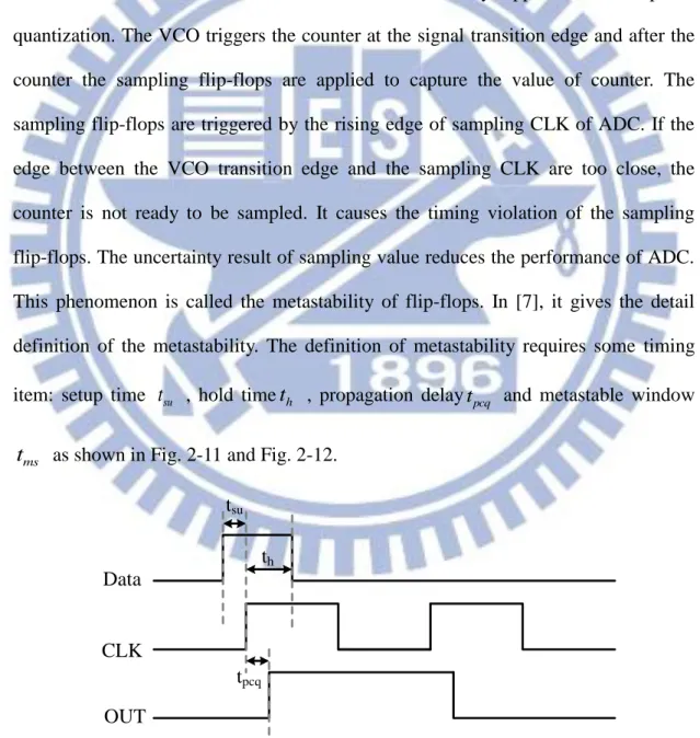
Metastability of flip-flops
For the VCO-based ADC, the counter is usually applied for the phase
quantization. The VCO triggers the counter at the signal transition edge and after the
counter the sampling flip-flops are applied to capture the value of counter. The
sampling flip-flops are triggered by the rising edge of sampling CLK of ADC. If the
edge between the VCO transition edge and the sampling CLK are too close, the
counter is not ready to be sampled. It causes the timing violation of the sampling
flip-flops. The uncertainty result of sampling value reduces the performance of ADC.
This phenomenon is called the metastability of flip-flops. In [7], it gives the detail
definition of the metastability. The definition of metastability requires some timing
item: setup time tsu , hold timeth , propagation delaytpcq and metastable window
ms
t as shown in Fig. 2-11 and Fig. 2-12.
Data CLK OUT tsu th tpcq
24
Max
Acceptable
t
pcqNormal
operation
t
pcqMetastability
window t
msPropagation delay t
pcqCLK as time
reference
Setup time
Hold time
CLK
Data
Fig. 2-12 Definition of metastability window
2-3
VCOs
In the barkhausen criteria it states that for negative-feedback circuit to oscillate at
0
its loop gain should satisfy the two conditions: 0 ( ) 1 H j (2.33) 0 ( ) 180 H j
(2.34)These conditions are necessary but not sufficient for oscillation. There are two
main topologies of CMOS oscillator in today’s technology: the ring VCO and the
inductance (L) and capacitance (C) VCO. LC VCO operates at the resonant frequency
of the inductor and capacitor while the ring VCO consists of a loop with an inversion
25
area for its passive elements and has poor integration and more complicated design.
And for the power performance, the ring VCO consumes less power than the LC VCO
at low oscillation frequency [8]. For above reasons, we choose the ring VCO for our
VCO-based ADC.
2-3.1 Ring oscillator basics
The ring oscillator consists of a delay cell loop which the output of the last cell
of the chain fed into the first element with an inversion net. Depending on the signal
in the loop, there are two kinds of architecture of ring oscillator: single-end and
differential ring oscillator. For both of two types the total inversion number should be
odd. As shown in Fig. 2-13, the single-end oscillator should have odd inversion stage
and for the differential oscillator the stage number can be odd or even but with a stage
connected inversely.
(a)
(b)
(c)
Fig. 2-13 Ring oscillators: (a) single-end oscillator (b) differential oscillator (odd
26
For all kinds of ring oscillators, the oscillation frequency is given by
equation(2.35). 1 *( ) : : : osc PHL PLH PHL PLH f N t t where N number of stage
t propagation delay of high to low transition t propagation delay of low to high transition
(2.35)
If we denote CL as the loaded capacitance in each node in delay chain which contains the total gate capacitance of input transistors, the total drain capacitance of
output transistors, the additional loading capacitance and the routing capacitance. The
delay for each stage is determined by the time for charging and discharging the
L
C .The time for discharging the CLfrom VDD to VSP with the constant ID1 is
1 1 L D
VDD VSP
t
C
I
(2.36)While the time for charging the CLfrom 0 to VDD with the constant ID2 is
2 2 L D
VSP
t
C
I
(2.37)Then we can find that tPHLand tPLHwe talked before is equal to t1 and t2
respectively when VSP is set to VDD/2. If we assumeID1ID2ID, the sum of
PHL
t and tPLHis shown as equation(2.38).
PHL PLH L D
VDD
t
t
C
I
(2.38)27 D osc L
I
f
N C
VDD
(2.39)In equation(2.39), it is clear that the oscillation frequency is controlled by stage
number N, the current ID, the loading capacitor CL and the supply voltage VDD. The stage number N is hard to be modulated by the analog signal. CL can be controlled by the varactor, but the linearity of this conversion is poor. Control VDD
will also affect the ID and the conversion has great linearity performance. We will take this type of oscillator into consideration for our design. ID can be controlled by the current-controlled cell which is the most basic type of ring oscillator structure and
the threshold voltage both of these two types of VCO will be simulated in the
following sections.
2-3.2 Jitter
In [9], it states the jitter prediction equation for single-end and differential ring
oscillator. First, it specifies a time window T which is defined as N cycles delay after triggering. Then it calculates the histogram of the crossing of the testing signal
during the window. The deviation of this histogram result is denoted as(T). Then we can find the relationship between standard deviation (T) and any delay T in equation(2.40). Other time domain measurement such as cycle jitter or cycle-to-cycle
jitter can be seen as the special case of the two-sample standard deviation. Although
we develop the result presenting in periods of signal cycle, the result is also valid
when developing in individual gate delays. The figure-of-merit
is the bridge connecting the jitter at any delay to a description of jitter process in one gate delay.28
( T)
T
(2.40)It also gives the jitter performance comparison between the single-end and
differential ring VCO. It denotes noise source has a voltage density of en [
V
/
Hz
] . The VCO has control constant K0 [rad/V*s] and the center frequency of
0 2 f
0. The
of both single-end and differential VCO is shown as below:Single-end ring VCO:
2 2 0 ( ) 0
2.00 2.66
DD0.50
n CTL DD t PK DDV
kT
K
e
V
V
I V
(2.41)Differential ring VCO:
2 2 0 ( ) 0
4.82 1.44
SWING0.50
n CTL DEGEN TAIL SWINGV
kT
K
e
V
I
V
(2.42)It states that for the best fundamental jitter performance, the single-end ring
VCO is preferred. Single-end ring VCO has several advantages shown as below:
A. Better jitter performance for given supply voltage since single-end ring has
larger swing than fully differential VCO. VSWING <VDD
B. Better jitter performance for given current since single-end ring has smaller
average current than fully differential VCO. Peak currentIPKonly occurs during the transition for single stage while bias current ITAIL flows in every stage continuously.
C. Single-end ring VCO doesn’t need the bias source, avoiding the additional
29
Chapter 3:
Proposed VCO-based differential
input ADC
3-1
Brief Architecture
Our VCO-based ADC architecture with differential input is shown in Fig. 3-1.
The input signals VIN+, VIN- modulate the VCO frequency individually. Two
counters are applied for both VCOs and quantize the frequency of VCO into digital
values. As considering power issue, asynchronous counter is applied for reducing the
dynamic power for data transition. To avoid sampling the counter value during
counter propagating, we use two group flip-flops to sample the counter for each
terminal and apply a determination circuit to choose the proper result. And also for the
power consideration, we use the flip-flop with gated input (G-FF) to reduce the spur
power. To avoid the metastability of flip-flop sampling, we disable the counter earlier
before sampling. The differential information is got by subtracting counter value of
each end. We design the circuit in UMC 90nm CMOS technology process. The details
30 Vin+ Vin-OUT CLK Counter G-FF D Q G-FF D Q +
-V alu e D ete rm in ati on C irc uit Counter G-FF D Q G-FF D Q V alu e D ete rm in ati on C irc uit Delay Line VCO VCOFig. 3-1 VCO-based ADC architecture
3-2
VCO Design
For the VCO-based ADC, VCO is the key component which has great influence
on the performance. Here, we choose the inverter-based ring VCO for simpler design
and smaller area. The basic invertor-based ring oscillator is shown as Fig. 3-2. Each
stage of ring oscillator is consisted of the invertor-like cell. According to the
introduction in section 2-3.1 , the frequency of ring oscillator is calculated as
1
(
)
osc PLH PHL D Lf
N t
t
I
N VDD C
(3.1)where CLis the input and output capacitance. In [10], it gives the digital model for the MOS transistor as shown in Fig. 3-4. In this model, it neglects the depletion
capacitance of source and drain implants to substrate. It assumes that both of the
gate-drain capacitance and gate-source capacitance is equal to half of Coxas shown in Fig. 3-3. Because the voltage across C changes by gd 2*VDD as gate change from 0 to VDD, C can be separated into the gate to ground and drain to ground capacitance gd
31
of value Cox. The total capacitance at the gate terminal is equal to 3
2Cox including
the gate-source capacitance1
2Cox and the drain to ground capacitance is equal to
ox
C .
Fig. 3-2 Invertor based ring oscillator
VDD Large resistor Drain voltage
initially at VDD
0
VDD
, 1 2 gd ox C C , 1 2 gs ox C C0
VDD
Fig. 3-3 MOSFET switching circuit with capacitance
outn ox C C 3 2 inn ox C C
Source
Gate
Rn
Drain
Fig. 3-4 Simple digital MOSFET model
32 3 3 ( ) ( ) 2 2 3 ( ) ( ) 2 5 ( ) 2 L in out p n p n ox p p n n ox p p n n p p n n C C C C C C C C W L W L C W L W L Cox W L W L (3.2)
We can see that the frequency of VCO can be influenced greatly by the
capacitance at the output of each stage which may change with the loading. To reduce
the frequency varying with the output loading, we can add the buffer to the output of
VCO. Here, we add an inverter as the buffer, whose loading is given as
3
( )
2C W Lox p pW Ln n .
For our specification shown in Table 1-1, the ENOB of ADC should be more
than 8 bits. For the margin of the quantization error and the non-ideal effect reducing
performance, we set the resolution of ADC to be 10 bits. Through the equation(2.11),
we can calculate the frequency requirement for our VCO is more than 10.24MHz. As
we introduce in section 2-2.5 , the nonlinearity of VCO is one of most important
characteristic should be cared about. We applied a simple DNL, INL test during VCO
design to characterize the linearity performance. Also, for our application, ECG
acquisition for mobile healthcare, the power of ADC should be considered, so power
consumption is also an issue for VCO chosen. Here we give some different types of
inverter based VCO delay cell for the ring structure VCOs. Their analysis and the
simulation results are shown below. And the chosen decision will be given in the end.
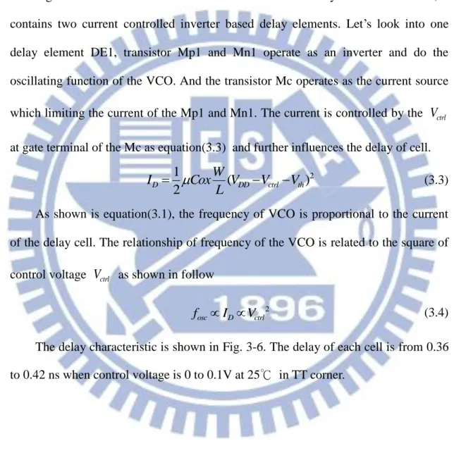
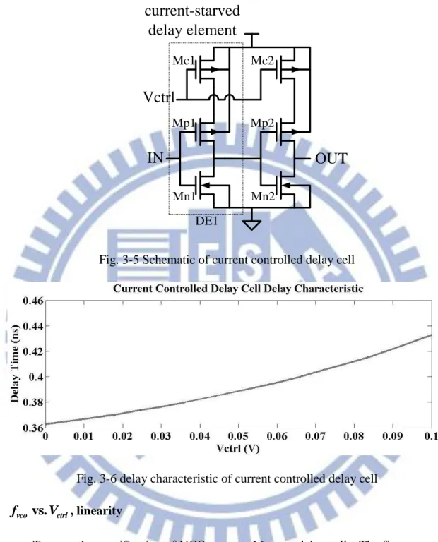
3-2.1 Current controlled delay cell
For the current control delay cell, the delay of current control delay cell is
33
MOS to modify the current of cell. In our application, the dc voltage of input signal is
in the relative low level, so we use the PMOS as the current control cell as shown in
Fig. 3-5.
Circuit description and Design Methodology
Fig. 3-5 shows the schematic of our current-starved delay cell. For each cell, it
contains two current controlled inverter based delay elements. Let’s look into one
delay element DE1, transistor Mp1 and Mn1 operate as an inverter and do the
oscillating function of the VCO. And the transistor Mc operates as the current source
which limiting the current of the Mp1 and Mn1. The current is controlled by the Vctrl
at gate terminal of the Mc as equation(3.3) and further influences the delay of cell.
2 1 ( ) 2 D DD ctrl th W I Cox V V V L
(3.3)As shown is equation(3.1), the frequency of VCO is proportional to the current
of the delay cell. The relationship of frequency of the VCO is related to the square of
control voltage Vctrl as shown in follow
2
osc D ctrl
f I V (3.4)
The delay characteristic is shown in Fig. 3-6. The delay of each cell is from 0.36
34
Vctrl
IN
OUT
Mc1 Mp1 Mn1 Mc2 Mp2 Mn2current-starved
delay element
DE1Fig. 3-5 Schematic of current controlled delay cell
Fig. 3-6 delay characteristic of current controlled delay cell
vs.
vco ctrl
f V , linearity
To meet the specification of VCO, we use 16 stage delay cells. The first stage of
the ring oscillator is implemented by the NAND gate for inversing the signal and the
start triggering. The overall VCO schematic is shown as Fig. 3-7. The frequency
performance is shown in Fig. 3-8. From equation (3.4) we can see that the control
linearity of current-starved delay cell is poor due to the square relation between
35
simple DNL and INL calculation for the frequency transfer line. To make the
comparison with other types of VCO faired, we set the LSBfreq as the frequency range divided by 100 as shown in equation(3.5). Due to the frequency transfer
function is got in 100 steps; LSBfreq is represented as the frequency resolution for each voltage step. The DNL of the current controlled ring VCO is 1.4625 LSB and
INL of this kind of VCO is 8.88 LSB which is really poor.
max( ) min( ) 100 freq f VCO f VCO LSB (3.5)
………
EN
V
ctrl15 stages
Fig. 3-7 Overall VCO schematic