1682 IEEE PHOTONICS TECHNOLOGY LETTERS, VOL. 23, NO. 22, NOVEMBER 15, 2011
Improved Performance of InGaN/GaN Light-Emitting
Diodes With Thin Intermediate Barriers
Bo-Chun Chen, Chun-Yen Chang, Yi-Keng Fu, Kai-Feng Huang, Yu-Hsuan Lu, and Yan-Kuin Su
Abstract—In this work, the performance of blue InGaN/GaN
light-emitting diodes (LEDs) with thin intermediate barriers at high injection current is investigated. From the experimental re-sults, it is found that the performance of LEDs with intermediate 5-nm-thick barriers is improved about 15% at 200 mA, compared with the sample with unique 9-nm-thick barriers. A numerical study is executed to analyze the hole distributions in the quantum wells. From the simulated results, it is found that the hole injection efficiency can be improved at high injection current. Hence, the effective recombination of electron and hole is also enhanced at high injection current.
Index Terms—Efficiency droop, internal quantum efficiency,
light-emitting diodes (LEDs).
I. INTRODUCTION
T
HE III-nitride light-emitting diodes (LEDs) have been extensively developed in many important applications due to the wide wavelength ranged from ultraviolet to green, such as the full-color displays, liquid-crystal display (LCD) backlighting, and solid-state lighting [1]–[6]. Nevertheless, the internal quantum efficiency (IQE) of InGaN/GaN multiple quantum wells (MQWs) LEDs decayed dramatically at high injection current. The unique phenomenon is called “efficiency droop”. To date, the major cause of efficiency droop is not clear and there is no effective method to solve this problem absolutely. Many possible mechanisms have been proposed to explain the behavior of efficiency droop, such as electron leakage from active regions due to polarization fields [1]–[3], Auger recombination process [4], defect density of substrate [2], and lack of hole in active regions due to the high effect mass and low mobility [6]–[8]. Besides, the formation of high barrier height in electron blocking layer (EBL) also retards the hole injection into the active regions [9]. To reduce efficiency droop, reduction of carrier leakage and poor transportation of hole injection play an important role for this issue. It wassug-Manuscript received July 15, 2011; revised August 15, 2011; accepted August 22, 2011. Date of publication August 30, 2011; date of current version October 21, 2011.
B.-C. Chen is with the Department of Electrophysics, National Chiao Tung University and Industrial Technology Research Institute, Hsinchu 300, Taiwan. (e-mail: [email protected]).
C.-Y. Chang is with the Department of Electronics Engineering, National Chiao Tung University, Hsinchu 300, Taiwan.
Y.-K. Fu is with the Industrial Technology Research Institute, Hsinchu 300, Taiwan.
K.-F. Huang is with the Department of Electrophysics, National Chiao Tung University, Hsinchu 300, Taiwan.
Y.-H. Lu and Y.-K. Su are with the Institute of Microelectronics, National Cheng Kung University, Tainan 701, Taiwan.
Color versions of one or more of the figures in this letter are available online at http://ieeexplore.ieee.org.
Digital Object Identifier 10.1109/LPT.2011.2166540
gested that asymmetric coupled InGaN quantum wells (QWs) active regions are used to improve hole transportation [10]. It has been reported that internal quantum efficiency is improved significantly when the typical undoped barriers are replaced by p-type GaN barriers [11].
II. DEVICESTRUCTURE
The blue InGaN/GaN LED used for this work was grown on a -plane sapphire substrate with Taiyo Nippon Sanso atmospheric pressure metal-organic chemical vapor deposi-tion (MOCVD) system. During the growth, trimethylgallium, trimethylindium, trimethylaluminum, and ammonia were used as the sources of Ga, In, Al, and N. After the thermal cleaning of sapphire substrate in hydrogen ambient for 10 minutes at 1080 C, the reference sample consisted of 25-nm-thick low-temperature nucleation layer, followed by a 2- m-thick undoped GaN layer grown at 1110 C, and a 2- m-thick Si-doped n-type GaN layer. It is worth to mention that the growth rates of undoped GaN and Si-doped n-type GaN were controlled to be 3.2 m hr. The active regions con-sisted of six 3-nm-thick InGaN quantum wells sandwiched by seven 9-nm-thick GaN barriers. After the active regions, a 25-nm-thick p-Al Ga N electron-blocking layer (EBL) and a 150-nm-thick p-GaN cap layer were deposited over the active regions. After the growth of LED structure, thermal acti-vation process was executed for 20 minutes at 750 C. By using the Hall measurement, the doping concentration of Si-doped GaN layer and Mg-doped GaN cap layer is near 3 cm and 4 cm , respectively. The Al composition in AlGaN layer is measured by performing HDXRD measurement. In addition, a transparent conduction indium-tin-oxide (ITO) was used as p-type Ohmic contact layer and Cr-Au metal was deposited as n- and p-type electrodes, respectively. The mesa area of the LED device geometry was 350 350 m .
In this work, hole injection efficiency and carriers recombina-tion of InGaN/GaN light-emitting diodes are studied in detail at high injection current, which the thicknesses of the barriers are decreased to be 5 nm in the intermediate three barriers. The ref-erence sample has unique barrier-thickness of 9 nm, which is la-beled as LED-I. For sample LED-II, the thicknesses of quantum barriers for LED structure, controlled by the growth time, are 15, 15, 5, 5, 5, 9, and 9 nm along [0001] direction. It is worth noting that the thicknesses of quantum wells are constant to be 3 nm and total thicknesses in the active regions are the same for these two LED samples.
III. EXPERIMENT ANDDISCUSSION
The LED devices were measured under room-temperature (RT) circumstance and light output power of LED chip on
CHEN et al.: IMPROVED PERFORMANCE OF InGaN/GaN LEDs WITH THIN INTERMEDIATE BARRIERS 1683
Fig. 1. Output powers of blue InGaN/GaN LEDs as a function of injection current.
Fig. 2. Simulated valence band diagrams at 200 mA.
TO-can was collected by using integrated sphere. Fig. 1 shows the light output power of the blue InGaN/GaN LEDs as a function of forward injection current. From the experimental results, the output powers of sample LED-II at 200 mA improve 15%, in compared with the sample LED-I.
In order to further study on the physical mechanisms respon-sible for the improvement of light output power in LED-II, the simulation software, SiLENSe 4.4 is used to perform numerical calculation for these two LED structures, especially for the hole distributions in active regions. For simulated LED structures, such as layer thicknesses, doping concentrations, Al composi-tion of EBL, In composicomposi-tion of quantum wells are as same as experimental structures.
Fig. 2 shows that the simulated valence energy band dia-grams of these two LED samples when injection current is 200 mA. In fact, hole Fermi-level distribution in the valence band is closely related to the hole distributions in the quantum
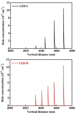
Fig. 3. Hole concentrations of the LEDs at 200 mA.
wells. If the hole Fermi-level can be efficiently covered under the valence band, it represents that more holes exist in the quantum wells. From the results of numerical calculation, the hole Fermi-level of sample LED-I is not covered efficiently under the valence band, especially for the quantum wells near the n-side layers. It reveals that the most holes accumulate in the quantum wells near p-side layers. To ameliorate this phenomenon of hole nonuniform, route reduction for holes from p-side layers to n-side layers perchance is a solution to resolve the hole nonuniform in quantum wells. To let more holes exist in the wells near n-side layers, the thicknesses of the intermediate three barriers are decreased from 9 nm to 5 nm. From the simulated results, hole Fermi-level is indeed covered efficiently under the valence band, especially for the last five quantum wells. It indicates that the hole existence of LED-II near n-side layers becomes more than that of LED-I at 200 mA. Fig. 3 show the hole concentration of the samples LED-I and LED-II in the quantum wells at 200 mA. As shown in Fig. 3, it’s found that the hole concentration decreases dramatically from p-side layers to active regions for sample LED-I. The reason why the phenomenon occurs is that low mobility forms a severe obstacle when holes transport into active regions. To enhance the hole injection efficiency, thin barriers are used to shorten the distance of hole transportation from p-side layers to quantum wells. As indicated in Fig. 3, the uniformity of hole distributions can be improved obviously after the thicknesses of intermediate three barriers are reduced from 9 nm to 5 nm. This phenomenon is consistent with the conjecture, which the holes injection effi-ciency can be enhanced by shortening the route from p-side to quantum wells.
1684 IEEE PHOTONICS TECHNOLOGY LETTERS, VOL. 23, NO. 22, NOVEMBER 15, 2011
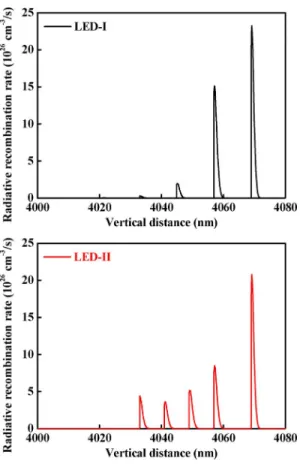
Fig. 4. Radiative recombination rates of the LEDs at 200 mA.
As shown in Fig. 4, the effective radiative recombination of electrons and holes in LED-I is primarily accumulated in the last two quantum wells, which means that the thick barriers have extreme retard for the transportation of holes into active regions. After the uniformity of hole distribution is improved, stronger radiative recombination also occurs in the intermediate quantum wells. The theoretical study on hole distribution and radiative recombination corresponds to the experimental results.
IV. CONCLUSION
In this letter, we have investigated the internal quantum ef-ficiency and droop efef-ficiency of LED device with intermediate thin barriers at high injection current. From the experimental results, it’s found that the employment of 5-nm-thick barriers in the intermediate three barriers can improve the light output
powers from 63.7 mW to 73.3 mW at 200 mA. In compar-ison between experimental and simulated results, the improve-ment of output power in LED device with intermediate three 5-nm-thick barriers is confirmed by using theoretical simula-tion. From simulated results, it’s found the use of thin barriers in intermediate locations, the uniformity of hole distribution can be also improved. In addition, the effective recombination of electron and holes in active regions is also increased.
REFERENCES
[1] M. H. Kim, M. F. Schubert, Q. Dai, J. K. Kim, E. F. Schubert, J. Piprek, and Y. Park, “Origin of efficiency droop in GaN-based light-emitting diodes,” Appl. Phys. Lett., vol. 91, pp. 183507-1–183507-3, Oct. 2007. [2] M. F. Schubert, S. Chhajed, J. K. Kim, E. F. Schubert, D. D. Koleske, M. H. Crawford, S. R. Lee, A. J. Fischer, G. Thaler, and M. A. Banas, “Effect of dislocation density on efficiency droop in GaInN/GaN light-emitting diodes,” Appl. Phys. Lett., vol. 91, pp. 231114-1–231114-3, Dec. 2007.
[3] M. F. Schubert, J. Xu, J. K. Kim, E. F. Schubert, M. H. Kim, S. Yoon, S. M. Lee, C. Sone, T. Sakong, and Y. Park, “Polariza-tion-matched CaInN/AlGaInN multi-quantum-well light-emitting diodes with reduced efficiency droop,” Appl. Phys. Lett., vol. 93, pp. 041102-1–041102-3, Jul. 2008.
[4] Y. C. Shen, G. O. Müller, S. Watanabe, N. F. Gardner, A. Munkholm, and M. R. Krames, “Auger recombination in InGaN measured by pho-toluminescence,” Appl. Phys. Lett., vol. 91, pp. 141101-1–141101-3, Oct. 2007.
[5] N. F. Gardner, G. O. Müller, Y. C. Shen, G. Chen, S. Watanabe, W. Götz, and M. R. Krames, “Efficient hole transport in asymmetric cou-pled InGaN multiple quantum wells,” Appl. Phys. Lett., vol. 95, pp. 161110-1–161110-3, Oct. 2009.
[6] J. Xie, X. Ni, Q. Fan, R. Shimada, U. Ozgur, and H. Morkoc, “On the efficiency droop in InGaN multiple quantum well blue light emitting diodes and its reduction with p-doped quantum well barriers,” Appl.
Phys. Lett., vol. 93, pp. 121107-1–121107-3, Sep. 2008.
[7] I. V. Rozhansky and D. A. Zakheim, “Analysis of processes limiting quantum efficiency of AlGaInN LEDs at high pumping,” Phys. Stat.
Sol. (a), vol. 204, pp. 227–230, Jan. 2007.
[8] I. A. Pope, P. M. Smowton, P. Blood, J. D. Thomson, M. J. Kappers, and J. Humphreys, “Carrier leakage in InGaN quantum well light-emit-ting diodes emitlight-emit-ting at 480 nm,” Appl. Phys. Lett., vol. 82, pp. 2755-1–2755-3, Mar. 2003.
[9] S. H. Han, D. Y. Lee, S. J. Lee, C. Y. Cho, M. K. Kwon, S. P. Lee, D. Y. Noh, D. J. Kim, Y. C. Kim, and S. J. Park, “Effect of electron blocking layer on efficiency droop in InGaN/GaN multiple quantum well light-emitting diodes,” Appl. Phys. Lett., vol. 94, pp. 231123-1–231123-3, Jun. 2009.
[10] C. H. Wang, S. P. Chang, W. T. Chang, J. C. Li, Y. S. Lu, Z. Y. Li, H. C. Yang, H. C. Kuo, T. C. Lu, and S. C. Wang, “Efficiency droop allevia-tion in InGaN/GaN light-emitting diodes by graded-thickness multiple quantum wells,” Appl. Phys. Lett., vol. 97, pp. 181101-1–181101-3, Nov. 2010.
[11] S. H. Han, C. Y. Cho, S. J. Lee, T. Y. Park, T. H. Kim, S. H. Park, S. W. Kang, J. W. Kim, Y. C. Kim, and S. J. Park, “Effect of Mg doping in the barrier of InGaN/GaN multiple quantum well on optical power of light-emitting diodes,” Appl. Phys. Lett., vol. 96, pp. 051113-1–051113-3, Oct. 2010.