100 EEE ELECTRON DEVICE LETTERS, VOL. 17, NO. 3, MARCH 1996
cation of Thin Film Transistors
by
olished Polycrystalline Silicon Films
Chun-Yen Chang,
Fellow, IEEE,Hsiao-Yi Lin,
Member, IEEE,Tan Fu Lei,
Juing-Yi Cheng, Liang-Po Chen, and Bau-Tong Dai,
Member, IEEEAbstract-A top-gate p-channel polycrystalline thin film tran-
sistor (TFT) has been fabricated using the polycrystalline silicon (poly-Si) film as-deposited by ultrahigh vacuum chemical vapor deposition (UHV/CVD) and polished by chemical mechanic& polishing (CMP). In this process, long-term recrystallization in channel films is not needed. A maximum field effect mobility of 58 cm2N-s, OWOFF current ratio of 1.1 lo7, and threshold voltage of -0.54 V were obtained. The characteristics are not poor. In
this work, therefore, we have demonstrated a new method to fabricate poly-Si TFT’s.
I. INTRODUCTION
OLYCRYSTALLINE silicon (poly-Si) thin film transis- tors (TFT’s) are widely used in various applications, such as three-dimensional (3-D) integrated circuits [ 11, image sen- sors [2], and active matrix liquid crystal displays (AMLCD’s) [3]. Recent advances in poly-Si TFT’s have spurred a great deal of interest because fabrication of poly-Si TFT’s on glass is a potential approach for AMLCD manufacturing. Poly- Si TFT’s provide a much higher carrier mobility than the amorphous silicon (a-Si) ones due to the fine film crystallinity, thus leading to faster switching speed and higher current driving capability. Unfortunately, the high-temperature and larger thermal budget processes encountered in conventional growth techniques of poly-Si films refrain from deposition on cheap glasses and restrict the development in this application. Therefore, it is essential to develop a low-temperature and low thermal budget process without compromising the device performance. In order to meet this requirement, lengthy re- crystallization treatment is often used, which may seriously affect the throughput of fabrication. Recently, it was found that the deposition at reduced pressures can obtain poly-Si below 550°C [4]-[6]. This finding makes fabricating poly-Si TFT’s at low-temperature and low thermal budget possible. Conventional gate oxide is still grown at high temperature, but high quality low-temperature oxide had been demonstrated by several papers [7]-[9]. Therefore, this work indicates the feasibility of using low temperature grown poly-Si for future full low temperature TFT fabrication process.
Manuscript received June 26, 1995; revised November 7, 1995. This work was supported by the National Science Council, Taiwan, Republic of China under Contract NSC-84-2215-E009-023.
C.-Y. Chang, H.-Y. Lin, T. F. Lei, and J.-Y. Cheng are with the Department of Electronics Engineering & Institute of Electronics, National Chiao Tung University and National Nan0 Device Laboratories, Hsinchu, 300 Taiwan, Republic of China.
L.-P. Chen and B.-T. Dai are with the National Nano Device Laboratories, Hsinchu, 300 Taiwan, Republic of China.
Publisher Item Identifier S 0741-3106(96)01962-3.
(b)
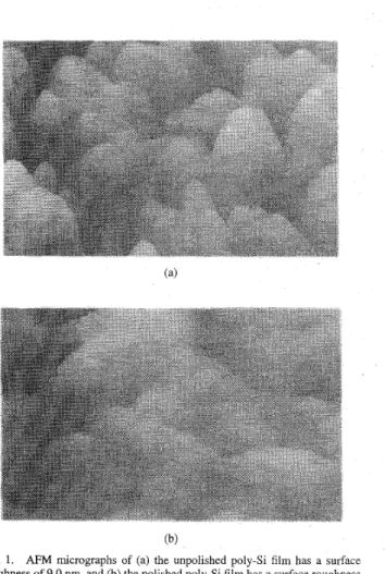
Fig. 1. AFM micrographs of (a) the unpolished poly-Si film has a surface
roughness of 9.0 nm, and (b) the polished poly-Si film has a surface roughness of 3.6 nm.
11. EXPERIMENT
In this work, we propose and demonstrate a new ap- proach for fabricating poly-Si TFT’ s. This approach utilizes an undoped poly-Si film to form the channel. An ultrahigh vacuum chemical vapor deposition (UHVKVD) system was employed to prepare the poly film followed by chemical mechanical polishing (CMP). These techniques feature an ultraclean growth environment, the reduced deposition pres- sures (-1 mTorr), and planarization technology. The CMP system was used to reduce the surface roughness of poly-Si films. In our previous works [5], [ 6 ] , we have shown that UHVKVD can deposit high quality fine-grain poly-Si films at temperatures below 550°C without further recrystalline
CHANG et al.: CHEMICAL MECHANICAL POLISHED POLYCRYSTALLINE SILICON FILMS 101
+
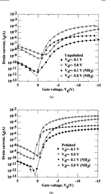
vd'- 0.1 V (unpolished) 0 vd'- 5.0 V (unpolished) A vd'- 0.1v
(polished) A vd'- 5.0v
(polished),
V I I I I 5 0 -5 -10 -15 Gate voltage, Vg(V)Fig. 2. Vpical drain current versus gate voltage of the polished and unpol- ished poly-Si TFT with a channel length of 20 pm and a channel width of
100 pm.
TABLE I
SUMMARY OF THE TFT CHARACTERISTICS SHOWN IN FIG 2 AND FIG 3
treatment, which is hard to achieve with the conventional low pressure chemical vapor deposition (LPCVD) processes. Therefore, the low-temperature poly-Si TFT is possible been fabricated by UHV/CVD. However, the drawback is the larger surface roughness inheres in these films[8], which inhibits the top-gate structure from fabricating self-aligned TFT's. Utilizing CMP to polish UHV/CVD deposited poly films, the surface roughness can be reduced and fabricating top-gate self-aligned TFT's at low temperature is possible.
In this study, a 150-mm silicon wafer coated with 300 nm-thick thermal grown oxide layer was used as the starting materials. An 160-nm thick and 120-nm thick undoped poly- Si films for polishing and comparison, respectively, were deposited on the thermal oxide by UHV/CVD at 550°C The undoped poly-Si was employed as the channel layer and its grain size was around 80 nm, as measured by the transmission electron microscopy (TEM). The 160-nm-thick poly-Si film was polished down to 120 nm by CMP. The uniformity of the poly thickness across 1.50-mm wafer before and after polishing are all within 10%. Then these films were defined by a photomask and patterned by plasma etching for the active area island, which have a thickness of 120 nm. A 30-nm thick gate oxide was then thermally grown at 850°C on the channel as the gate dielectric. After these steps, a 300-nm thick undoped poly-Si was deposited by UHV/CVD at 550°C as the gate material, which was also defined by a photomask patterning and by plasma etching. The gate-electrode and source/drain
5 0 -5 -10 -15 Gate voltage, Vg(V) (a) 10-2 I I I I I I I 10-8 10-9 10-10 10-11 10-12 I I I 5 0 -5 -10 -15 Gate voltage, V,(V) (b) Fig. 3 .
with and without NH3 plasma treatment.
The comparison of (a) unpolished and (h) polished poly-Si TFT's
regions were doped by boron implantation at
a
energy of 20 keV and a dose of 3 x 1015 cm-2. After implantation, a 550°C anneal was given at N2 ambient for 1 h. The resistivity is around 3 m k m . The 200-nm thick oxide passivation-layer was deposited by plasma enhanced chemical vapor deposition (PECVD) system at 300°C. Finally, contact hole definition and A1 metalization was performed. After these processes, a NH3 plasma treatment was given.111. DISCUSSION
The roughnesses of the poly film observed by atomic force microscope (AFM) were shown in Fig. l(a) and Fig. l(b)
for unpolished and polished ones, respectively. We found that the RMS surface roughness of the poly film had been dramatically reduced from 9.0 nm to 3.7 nm after polishing. Typical transfer curves are shown in Fig. 2 and Fig. 3. Fig. 2 illustrates the I-V Characteristics of polished and unpolished devices with a channel length of 20 pm and
a
width of 100102 IEEE ELECTRON DEVICE LETTERS, VOL. 17, NO. 3, MARCH 1996
pm. For the polished device, ION is around 500 pA (at the gate voltage, Vq = -15 V),
I O F F
is around 300 pA (at the drain current is minimum), andI O N / I O F F
z 1.5x
lo6.
The subthreshold swing is 0.4.5 V/decade and threshold voltage is -4.2 V. However, the characteristics of unpolished device is very poor. The greatly improved transistor characteristics were not only due to the improvement in mobility, but also the significantly reduced gate leakage current due to reduction of surface roughness which degrades the ON current and also OFF characteristics. In addition, the oxidation ambient can slightly alter the morphology of the film, which also enhances the gate leakage current in unpolished devices. Fig. 3(a) shows the transfer curves of unpolishedTFT’s with
and without NH3 treatment, which has a maximum field effect mobility 7.5 cm2N.s even if NHs plasma treatment. Fig. 3(b) shows the transfer curves of polished TFT’s with and without NH3 treatment, which has a maximum field effect mobility 58 cm2N.s after NH3 plasma treatment. More device characteristics were summarized in Table I. A detailed investigation and improvement of the device performance is underway, and will be presented in the near future.IV. CONCLUSION
In summary, we have developed a new process for fabri- cating poly-Si TFT’s using UHV/CVD and CMP techniques and demonstrated the performance. Our results reveal that the usage of these techniques on the device fabrication would be a possible approach to reach low-temperature, low ther- mal budget, and high throughput process steps. To further improve the device performance, developing high quality low-temperature oxides are essential to obtain the real low temperature processed devices.
ACKNOWLEDGMENT
The authors would like to express their appreciation to all staffs of Semiconductor Research Center, National Chiao Tung University for their technical support.
REFERENCES
S. D. S. Malhi, H. Shichijo, S. K. Banerjee, R. Sundaresan, M. Elahy, G. P. Pollack, W. F. Richardson, A. H. Shah, L. R. Hite, R. H. Womack, P. K. Chatterjee, and H. W. Lam, “Characteristics and three-dimentional integration of MOSFETs in small-grain LPCVD polycrystalline silicon,”
IEEE Trans. Electron Devices, vol. 32, pp. 258-281, 1985.
S. Morozumi, H. Kurihara, T. Takeshita, H. Oka, and K. Hasegawa, “Completely integrated contact-type linear image sensor,” IEEE Trans. Electron Devices, vol. 32, pp. 1546-1550, 1985.
H. Ohshima and S. Morozumi, “Future trends for TFT integrated circuits on glass substrates,” IEDM Tech. Dig. 89, p, 157, 1989.
A. T. Voultsas and M. K. Hatalis, “Structure of as-deposited LPCVD sili- con films at low deposition temueratures and pressures,” J. Electrochem.
Soc. vol. 139, p. i659, 1992. ~
H. C. Lin, H. Y . Lin, C. Y . Chang, T. F. Lei, P. J. Wang, and
C. Y . Chao, “Growth of undoped polycrystalline Si by an ultra-high vacuum chemical vauor deuosition system,” A d .
_ _
Phvs. , Lett. vol. 63.pp. 1351-1353, 199i. ~
H. C. Lin, H. Y . Lin, C. Y . Chang, T. F. Lei, P. J. Wang, R. C . Deng,
J. Lin, and C. Y . Chao, “Deposition and device application of in situ boron-doped polycrystalline SiGe films grown at low temperatures,” J. Appl. Phys. vol. 74, p. 5395, 1993.
Y . Nishi, T. Funai, H. Izawa, T. Fujimoto, H. Morimoto, and M. Ishii, “Characteristics of plasma-enhanced-chemical-vapor-deposition tetraethylorthosilicate oxide and thin-film-transistor application,” Jpn.
J. Appl. Phys. vol. 31 no. 12B, p. 45i’b,1992.
N. Yamauchi, N. Kakuda, and T. Hisaki, “Characteristics of high mo- bility polysilicon thin-film transistors using very thin sputter-deposited Si02 films,” IEEE Trans. Electron Devices, vol. 41, pp. 1882-1885,
1994.
A. Kohno, T. Sameshima, N. Sano, M. Sekiya, and M. Hara, “High performance poly-Si TFT’s fabricated using pulsed laser annealing and remote plasma CVD with low temperature processing,” IEEE Trans. Electron Devices, vol. 42, pp. 251-257, 1995.