Highly scaled charge-trapping layer of ZrON nonvolatile memory device with good
retention
C. Y. Tsai, T. H. Lee, C. H. Cheng, Albert Chin, and Hong Wang
Citation: Applied Physics Letters 97, 213504 (2010); doi: 10.1063/1.3522890
View online: http://dx.doi.org/10.1063/1.3522890
View Table of Contents: http://scitation.aip.org/content/aip/journal/apl/97/21?ver=pdfcov Published by the AIP Publishing
Articles you may be interested in
Formation of iridium nanocrystals with highly thermal stability for the applications of nonvolatile memory device with excellent trapping ability
Appl. Phys. Lett. 97, 143507 (2010); 10.1063/1.3498049
Device characteristics of HfON charge-trap layer nonvolatile memory J. Vac. Sci. Technol. B 28, 1005 (2010); 10.1116/1.3481140
Optical capacitance-voltage characterization of charge traps in the trapping nitride layer of charge trapped flash memory devices
Appl. Phys. Lett. 91, 223511 (2007); 10.1063/1.2819092
Impact of high-pressure deuterium oxide annealing on the blocking efficiency and interface quality of metal-alumina-nitride-oxide-silicon-type flash memory devices
Appl. Phys. Lett. 91, 192111 (2007); 10.1063/1.2812570
Memory characteristics of silicon nitride with silicon nanocrystals as a charge trapping layer of nonvolatile memory devices
Appl. Phys. Lett. 86, 251901 (2005); 10.1063/1.1951060
This article is copyrighted as indicated in the article. Reuse of AIP content is subject to the terms at: http://scitation.aip.org/termsconditions. Downloaded to IP: 140.113.38.11 On: Wed, 30 Apr 2014 09:54:25
Highly scaled charge-trapping layer of ZrON nonvolatile memory device
with good retention
C. Y. Tsai,1T. H. Lee,1C. H. Cheng,1Albert Chin,1,a兲and Hong Wang2
1Department of Electronics Engineering and Institute of Electronics, National Chiao-Tung University,
Hsinchu 30010, Taiwan
2School of Electrical and Electronic Engineering, Nanyang Technological University, Singapore 639798
共Received 2 August 2010; accepted 5 November 2010; published online 24 November 2010兲 We have fabricated the TaN–关SiO2– LaAlO3兴–ZrON–关LaAlO3– SiO2兴–Si charge-trapping flash device with highly scaled 3.6 nm equivalent-Si3N4-thickness. This device shows large 4.9 V initial memory window, and good retention of 3.4 V ten-year extrapolated retention window at 85 ° C, under very fast 100 s and low⫾16 V program/erase. These excellent results were achieved using deep traps formed in ZrON trapping layer by As+ implantation that was significantly better than those of control device without ion implantation. © 2010 American Institute of Physics.
关doi:10.1063/1.3522890兴
As listed in International Technology Roadmap for
Semiconductors,1 the metal-oxide-nitride-oxide-Si 共MONOS兲 charge-trapping flash 共CTF兲 devices1–15
have high potential to replace the poly-Si floating-gate flash memory for future generation nonvolatile memory共NVM兲 due to the discrete charge-trapping property and simpler planar process. Nevertheless, one fundamental drawback for CTF device is the distributed trap energy in Si3N4 共Ref. 11兲 as compared with the deep 3.15 eV energy in poly-Si floating-gate memory, where charge stored in shallower traps may escape and degrade the retention characteristics.12–15Such degraded retention is one of the major challenges in fewer electrons stored in highly scaled NVM device.1 Although improved retention can be achieved by increasing tunnel oxide thick-ness, this is traded off the intolerable slow erase time 共10– 100 ms兲.
One method to improve the retention is to use a deep conduction band energy共EC兲 high-trapping layer.12–16 Sig-nificant retention improvement has been realized by using high-Al共Ga兲N in the MONOS CTF that was also listed in ITRS as a key technology for CTF.1 To further lower the program/erase 共P/E兲 voltage, higher HfON trapping layer MONOS has been fabricated,14 but the shortcoming is the lower trapping efficiency in HfON with a smaller memory window.14 To improve the memory window, dual trapping-layer HfON– Si3N4 CTF was used,15 but adding the lower
Si3N4 limits further down-scaling the equivalent-nitride thickness共ENT兲. However, scaling ENT to 3–4 nm is needed for future CTF NVM.1Alternatively, lower trapping energy can also be reached by forming nanocrystal in CTF using ion implantation.17–20 In this paper we have used both higher- deep-EC ZrON and As+ implantation to improve the CTF performance. At a 3.6 nm ENT trapping layer, this device has an initial 4.9 V memory window and good retention of 3.4 V extrapolated ten-year retention window at 85 ° C, under fast 100 s and low⫾16 V P/E. This is the thinnest ENT CTF device that meets ITRS scaling target to tenth nanometer.1
The TaN–关SiO2– LaAlO3兴–ZrON–关LaAlO3– SiO2兴–Si devices were fabricated on standard 6 in. p-type Si wafers. The double tunnel oxide layers of 2.5 nm thermal SiO2were
grown on Si substrates and 2.5 nm LaAlO3was deposited by physical vapor deposition 共PVD兲. Then the 18 nm ZrON charge trapping layer was deposited by reactive PVD under mixed O2and N2. The As+-implantation into ZrON was ap-plied at 3 keV, 5⫻1015 cm−2 dose, and 60° titled angle, which was followed by 950 ° C and 1 s rapid thermal anneal-ing 共RTA兲. It was reported that the memory window in-creases with increasing ion-implanted dose.20 The As+-implant condition of 5⫻1015 cm−2 and 3 keV dose were chosen to reach both the highest possible dose for manufacture and the lowest energy for the thinnest ENT. Next, 8 nm LaAlO3was deposited by PVD and 6 nm SiO2 was deposited by chemical vapor deposition of tetraethyl orthosilicate 关Si共C2H5O兲4兴 to form the double blocking lay-ers. Finally, 200 nm TaN was deposited by PVD, followed by gate definition, self-aligned 25 keV As+ implantation at 5 ⫻1015 cm−2dose, and 900 ° C RTA to activate the dopant at source-drain region. The flatband voltage共VFB兲 was obtained from the measured C-V data and quantum-mechanical C-V simulation.21 The threshold voltage 共Vth兲 was determined from the interception of gate voltage共Vg兲 to zero drain cur-rent 共Id兲 of linear Id-Vgcurve.
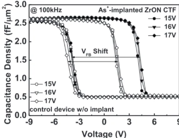
Figure1compares C-V hysteresis of ZrON CTF devices with and without the As+implantation. Larger C-V hysteresis window of 8.1 V was obtained in As+-implanted CTF than
a兲Electronic mail: albert_achin@hotmail.com.
-9 -6 -3 0 3 6 9 0.0 0.5 1.0 1.5 2.0 2.5 3.0 @ 100kHz VFBShift 15V 16V 17V
control device w/o implant
As+-implanted ZrON CTF C a p a c ita n c e D e n s ity (fF / m 2 ) Voltage (V) 15V 16V 17V
FIG. 1. C-V hysteresis of ZrON CTF devices with and without As+
implantation.
APPLIED PHYSICS LETTERS 97, 213504共2010兲
0003-6951/2010/97共21兲/213504/3/$30.00 97, 213504-1 © 2010 American Institute of Physics
This article is copyrighted as indicated in the article. Reuse of AIP content is subject to the terms at: http://scitation.aip.org/termsconditions. Downloaded to IP: 140.113.38.11 On: Wed, 30 Apr 2014 09:54:25
the 5.7 V of control device under ⫾16 V sweep and close capacitance density of⬃2.6 fF/m2for both devices. Since the area of C-V curve is the charge共Q=CV兲, the increase of
VFB indicates that the As+-implanted ZrON has higher trap density for electron storage. The larger hysteresis window by As+ implantation may be due to the forming deep energy levels in ZrON trapping layer that exists even after 950 ° C RTA. From the frequency-dependent C-V measurements, the
VFB shift 共⌬VFB兲 is independent on frequencies at 10–700 kHz. Thus, the hysteresis memory window is only from the ZrON trapping layer rather than the interface states between tunnel oxide and Si.
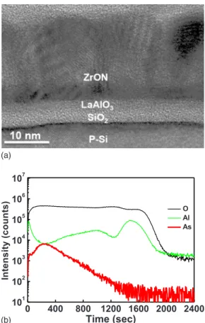
Figures2共a兲and2共b兲show the cross-sectional transmis-sion electron microscopy 共TEM兲 and secondary ion-mass spectroscopy 共SIMS兲 of ZrON–关LaAlO3– SiO2兴–Si struc-ture with As+ implantation. The polygrains were found in ZrON after 950 ° C RTA that leads to the higher value22,23 with As+implant. From the measured 18 nm ZrON thickness by TEM, an ENT of 3.6 nm was obtained from the ENT =Si3N4/ZrON⫻tZrON, where theSi3N4,ZrON, and tZrONare the dielectric constant of Si3N4, dielectric constant of ZrON, and the thickness of ZrON, respectively. The concentration of implanted As decreases rapidly before entering the double tunnel layer of LaAlO3-SiO2. Such low energy tilted-angle As+implantation is important to reduce the damage to tunnel oxide layer.
Figure 3 shows the x-ray diffraction 共XRD兲 spectra of ZrON–关LaAlO3– SiO2兴–Si structure with and without As+ implantation. The strong diffraction peaks indicate the good ZrON crystallinity that is important to provide higher ⬃35 共Refs.22 and23兲 with a smaller ENT of 3.6 nm.
Be-sides, extra weak As peaks were also found in As+-implanted
and 950 ° C-annealed ZrON, with the same angles of clus-tered As-dots in As-rich GaAs.24This suggests the possibility to form the deep energy levels in ZrON due to large As work-function of 5.1 eV,25 which also explains the larger hysteresis shown in Fig. 1.
Data retention is one of the most importance parameters for NVM. Figure 4 shows the retention characteristics at 85 ° C. Under ⫾16 V and 100 s P/E, the As+-implanted ZrON devices have a larger initial memory window of 4.9 V than the 2.9 V data of control device without As+ implanta-tion, suggesting the higher trap density in As+-implanted ZrON trapping layer. The very fast 100 s P/E speed is due to the additional conduction and valance band disconti-nuity 共⌬EC and⌬EV兲 between LaAlO3 and SiO2, for easier electron and hole tunneling during program and erase, re-spectively. Still large ten-year extrapolated memory window of 3.4 V was obtained for As+-implanted ZrON CTF device and better than that of control device. The good retention is due to the physically thicker double LaAlO3– SiO2for carrier confinement, while the ⌬EC and ⌬EV in LaAlO3/SiO2 im-prove the program and erase speed. This large ten-year re-tention window with a small 3.6 nm ENT trapping layer also allows multilevel cell storage at 85 ° C.15
In summary, we have used both higher ZrON and As+ implantation to improve the device performance of MONOS CTF device. At record smallest 3.6 nm ENT, large 4.9 V initial memory window and good retention of 3.4 V ten-year extrapolated window at 85 ° C were measured in this CTF
0 400 800 1200 1600 2000 2400 101 102 103 104 105 106 107 Int ens ity (c o u nt s) Time (sec) O Al As (b) (a)
FIG. 2. 共Color online兲 共a兲. Cross-sectional TEM and 共b兲 SIMS of ZrON–关LaAlO3– SiO2兴–Si structure with As+implantation.
20 30 40 50 60 70 0 100 200 300 400 As(003) ZrO2(220) ZrO 2(103) As(012) ZrO 2(200) ZrO2(111)
control un-implanted ZrON As+-implanted ZrON Int ens ity (co u nt s ) 2 (degree)
FIG. 3. 共Color online兲 XRD of ZrON–关LaAlO3– SiO2兴–Si structure with
and without As+implantation.
100 102 104 106 108 -3 -2 -1 0 1 2 3 4 5 P/E: 16V 100s As+-implanted un-implanted 2.1V 2.9V 3.4V 85o C 4.9V 85o C 10 years Vth (V ) Time (sec)
FIG. 4. Retention characteristics of ZrON MONOS CTF devices at 85 ° C with and without As+implantation.
213504-2 Tsai et al. Appl. Phys. Lett. 97, 213504共2010兲
This article is copyrighted as indicated in the article. Reuse of AIP content is subject to the terms at: http://scitation.aip.org/termsconditions. Downloaded to IP: 140.113.38.11 On: Wed, 30 Apr 2014 09:54:25
device, under very fast 100 s speed and low P/E voltage of ⫾16 V.
The paper publication was supported by National Sci-ence Council of Taiwan under Project No. NSC99–2120–M-009–002
1Seewww.itrs.netfor The International Technology Roadmap for
Semicon-ductors共ITRS兲, 2009.
2S.-I. Minami and Y. Kamigaki,IEEE Trans. Electron Devices 40, 2011
共1993兲.
3M. H. White, Y. Yang, A. Purwar, and M. L. French,IEEE Trans. Com-pon., Packag. Manuf. Technol., Part A 20, 190共1997兲.
4M. She, H. Takeuchi, and T.-J. King, Proceedings of the IEEE Nonvolatile
Semiconductor Memory Workshop, 2003, p. 53.
5C. H. Lee, K. I. Choi, M. K. Cho, Y. H. Song, K. C. Park, and K. Kim,
Tech. Dig. - Int. Electron Devices Meet. 2003, 613.
6C. W. Oh, S. D. Suk, Y. K. Lee, S. K. Sung, J.-D. Choe, S.-Y. Lee, D. U.
Choi, K. H. Yeo, M. S. Kim, S.-M. Kim, M. Li, S. H. Kim, E.-J. Yoon, D.-W. Kim, D. Park, K. Kim, and B.-I. Ryu, Tech. Dig. - Int. Electron Devices Meet. 2004, 893.
7M. Specht, R. Kommling, L. Dreeskornfeld, W. Weber, F. Hofmann, D.
Alvarez, J. Kretz, R. J. Luyken, W. Rosner, H. Reisinger, E. Landgraf, T. Schulz, J. Hartwich, M. Stadele, V. Klandievski, E. Hartmann, and L. Risch, Symposium on VLSI Technology Digest共IEEE, New York, 2004兲, p. 244.
8X. Wang, J. Liu, W. Bai, and D.-L. Kwong,IEEE Trans. Electron Devices
51, 597共2004兲.
9Y. N. Tan, W. K. Chim, W. K. Choi, M. S. Joo, T. H. Ng, and B. J. Cho,
Tech. Dig. - Int. Electron Devices Meet. 2004, 889.
10X. Wang and D.-L. Kwong,IEEE Trans. Electron Devices 53, 78共2006兲. 11S. H. Gu, T. Wang, W. P. Lu, Y. H. Ku, and C. Y. Lu,Appl. Phys. Lett. 89,
163514共2006兲.
12C. H. Lai, Albert Chin, K. C. Chiang, W. J. Yoo, C. F. Cheng, S. P.
McAlister, C. C. Chi, and P. Wu, Symposium on VLSI Technology Digest 共IEEE, New York, 2005兲, p. 210.
13Albert Chin, C. C. Laio, K. C. Chiang, D. S. Yu, W. J. Yoo, G. S.
Sam-udra, S P. McAlister, and C. C. Chi, Tech. Dig. - Int. Electron Devices Meet. 2005, 165.
14C. H. Lai, Albert Chin, H. L. Kao, K. M. Chen, M. Hong, J. Kwo, and C.
C. Chi, Symposium on VLSI Technology Digest共IEEE, New York, 2006兲, p. 54.
15S. H. Lin, Albert Chin, F. S. Yeh, and S. P. McAlister, Tech. Dig. - Int.
Electron Devices Meet. 2008, 843.
16K. H. Joo, C. R. Moon, S. N. Lee, X. Wang, J. K. Yang, I. S. Yeo, D. Lee,
O. Nam, U. I. Chung, J. T. Moon, and B. I. Ryu, Tech. Dig. - Int. Electron Devices Meet. 2006, 979.
17E. Kapetanakis, P. Normand, D. Tsoukalas, K. Beltsios, J. Stoemenos, S.
Zhang, and J. van den Berg,Appl. Phys. Lett. 77, 3450共2000兲.
18S. M. Choi, H. D. Yang, M. Chang, S. K. Baek, H. S. Hwang, S. H. Jeon,
J. Y. Kim, and C. W. Kim,Appl. Phys. Lett. 86, 251901共2005兲.
19C. J. Park, K. H. Cho, W.-C. Yang, H. Y. Cho, S.-H. Choi, R. G. Elliman,
J. H. Han, and C. Kim,Appl. Phys. Lett. 88, 071916共2006兲.
20M. C. Kim, S. H. Hong, H. R. Kim, S. Kim, S.-H. Choi, R. G. Elliman,
and S. P. Russo,Appl. Phys. Lett. 94, 112110共2009兲.
21S. H. Lin, C. H. Cheng, W. B. Chen, F. S. Yeh, and A. Chin, IEEE Electron Device Lett. 30, 999共2009兲.
22S. H. Lin, K. C. Chiang, A. Chin, and F. S. Yeh,IEEE Electron Device Lett. 30, 715共2009兲.
23C. Y. Tsai, K. C. Chiang, S. H. Lin, K. C. Hsu, C. C. Chi, and A. Chin, IEEE Electron Device Lett. 31, 749共2010兲.
24R. R. Campomanes, J. Vilcarromero, J. C. Galzerani, and J. H. Dias Da
Silva,Appl. Phys. A: Mater. Sci. Process. 80, 267共2005兲.
25H. B. Michaelson,J. Appl. Phys. 48, 4729共1977兲.
213504-3 Tsai et al. Appl. Phys. Lett. 97, 213504共2010兲
This article is copyrighted as indicated in the article. Reuse of AIP content is subject to the terms at: http://scitation.aip.org/termsconditions. Downloaded to IP: 140.113.38.11 On: Wed, 30 Apr 2014 09:54:25