IEEE PHOTONICS TECHNOLOGY LETTERS, VOL. 23, NO. 19, OCTOBER 1, 2011 1373
Study of InGaN-Based Light-Emitting Diodes on a
Roughened Backside GaN Substrate by a Chemical
Wet-Etching Process
Yi-Keng Fu, Bo-Chun Chen, Yen-Hsiang Fang, Ren-Hao Jiang, Yu-Hsuan Lu, Rong Xuan, Kai-Feng Huang,
Chia-Feng Lin, Yan-Kuin Su, Jebb-Fang Chen, and Chun-Yen Chang
Abstract—The InGaN-based light-emitting diodes (LEDs) with a roughened backside on the N-face surface of GaN substrate were fabricated through a chemical wet-etching process to in-crease light-extraction efficiency. The stable crystallographic etching planes were formed as the GaN planes. When the near-ultraviolet and blue LED were operated as a forward current of 20 mA, the output power of LEDs was improved from 13.2 and 19.9 mW to 25.6 and 24.0 mW, respectively. The different enhanced ratio is attributed to the different transmittance as a function of wavelength is caused from hexagonal pyramid on N-face GaN substrate after wet-etching process.
Index Terms—Chemical wet-etching, GaN, light extraction, near-ultraviolet (NUV) light-emitting diode (LED).
I. INTRODUCTION
R
ECENTLY, tremendous progress has been achieved in GaN-based blue, green and ultraviolet light emitting diodes (LEDs) [1], [2]. These nitride-based LEDs are also potentially useful for solid-state lighting. To realize solid-state lighting, however, one needs to further improve output ef-ficiency of these LEDs. It is known that light-extraction efficiency of GaN-based LED is limited mainly by the large difference in refractive index between GaN film and the sur-rounding air. The critical angle for photons to escape from GaN film is determined by Snell’s law. The angle is crucially important for the light-extraction efficiency of LEDs. Since the refractive indexes of GaN and air are 2.5 and 1, respectively, external quantum efficiency was limited to only a few percents for conventional GaN-based LEDs. It has been demonstratedManuscript received April 21, 2011; revised May 30, 2011; accepted June 24, 2011. Date of publication July 07, 2011; date of current version September 09, 2011.
Y.-K. Fu is with the Opto-Electronics Epitaxy and Device Department, Industrial Technology Research Institute, Hsinchu 31040, Taiwan (e-mail: [email protected]).
B.-C. Chen, R. Xuan, K.-F. Huang, and J.-F. Chen are with the Electrophysics Department, National Chiao-Tung University, Hsinchu 300, Taiwan.
Y.-H. Fang is with Electronics and Optoelectronics Research Laboratory, In-dustrial Technology Research Institute, Hsinchu 31040, Taiwan.
R.-H. Jiang and C.-F. Lin are with the Department of Materials Science and Engineering, National Chung Hsing University, Taichung 402, Taiwan.
Y.-H. Lu is with Institute of Microelectronics, National Cheng-Kung Univer-sity, Tainan City 701, Taiwan.
Y.-K. Su is with the Department of Electrical Engineering, National Cheng Kung University, Tainan 70101, Taiwan.
C.-Y. Chang is with the Department of Electronics Engineering, National Chiao Tung University, Hsinchu 300, Taiwan.
Color versions of one or more of the figures in this letter are available online at http://ieeexplore.ieee.org.
Digital Object Identifier 10.1109/LPT.2011.2161276
that several methods can be used to improve light-extraction efficiency in InGaN-based LEDs on Al O substrate, such as bottom patterned Al O substrate [3], top p-type GaN:Mg rough surface processes [4], [5], the formation of photonic crystal structure [6], [7] and selective oxidization on the mesa sidewall through a photoelectrochemical (PEC) wet oxidation process [8]. Among these, PEC etching has advantages in terms of the compatibility with conventional semiconductor processing equipment and easy scalability to large wafers as well as the processing cost.
H. M. Ng et al. have reported the formation of GaN nanotip pyramids by selective and anisotropic etching of N-polar GaN in Potassium Hydroxide (KOH) solution [9]. An aggregation of hexagonal pyramids with defined facets and very sharp tips were formed. A similar concept could also be applied to the applications of GaN substrate. In other words, we might be able to enhance the LED output power by textured backside of the LEDs. In this study, InGaN-based near-ultraviolet (n-UV) and blue LEDs were grown on GaN substrate, respectively. Detailed fabrication process, numerical demonstrations, and the proper-ties of fabricated LEDs will also be discussed
II. EXPERIMENT
The n-UV and blue InGaN/GaN LEDs used in this study were all grown on c-face (0001) 2-inch GaN substrates in a SR-4000 atmospheric pressure metal–organic chemical vapor deposition system. GaN substrates were fabricated by C. L. Chao et al. group [10]. LED structure consists of a 4- m-thick Si-doped GaN n-cladding layer, an multi quantum well (MQW) active layer, a 20-nm-thick p-type Mg-doped Al Ga N layer and a 200-nm-thick Mg-doped GaN layer. The MQW active region consists of five periods of 2.4-nm-thick undoped In Ga N well layer and 9-nm-thick undoped GaN barrier layer. During the MQW growth, the growth temperature was modulated in order to adjust the peak wavelength of LED. The peak wavelength of these n-UV and blue LED was 405 and 450 nm, respectively. For the fabrication of LEDs, indium tin oxide (ITO) was first deposited on these LEDs as a transparent contact layer (TCL). Then, we partially etched the surface of the samples until the n-type GaN layers were exposed. We subsequently deposited Cr/Au onto the exposed n-type and p-type GaN layer to serve as the n-type and p-type electrode. The chip size of LEDs was 375 m 375 m.
After chip processes, the epitaxial wafers were then lapped down to about 110 m. We subsequently placed these samples into a hot 2-M KOH solution without any stirring to form in
1374 IEEE PHOTONICS TECHNOLOGY LETTERS, VOL. 23, NO. 19, OCTOBER 1, 2011
Fig. 1. Schematic diagrams of the LED structure with a roughened backside on the N-face GaN substrate surface.
Fig. 2. The 30 tile-view and cross-sectional (inset) SEM images of the sur-face morphology on N-sur-face GaN substrate at 80 C in various times of KOH solutions (a) before etching, (b) 1 min, (c) 5 min, (d) 10 min, (e) 30 min, and (f) 60 min.
the pyramidal structure at the N-face GaN substrate. During wet-etching process, we used etching time (10 min) at 80 C. We then used scribe and break to complete the fabrication of LEDs. The schematic of the LED structure and the process steps are shown in Fig. 1. The LED device that was fabri-cated through this process flow without and with a chemical wet-etching process was defined as a standard LED (ST-LED), and a roughened backside LED (RB-LED), respectively. The n-UV and blue LEDs were defined as LED I (including the ST-LED I and RB-LED I) and LED II (including the ST-LED II and RB-LED II), respectively. The geometric morphology of these LED structures was observed through a scanning electron microscopy (SEM). These chips were p-sideup-mounted on a Ag TO-46 and molded in epoxy resin. We measured their room temperature (RT) current–voltage ( – ) characteristics by an HP4156 semiconductor parameter analyzer. Light output power–current ( – ) characteristics of these fabricated LEDs were also measured using the molded LEDs with the integrated sphere detector. To minimize heating effect, the injection current was a pulsed current source with 1% duty cycle and 10 kHz frequency.
III. RESULTS ANDDISCUSSION
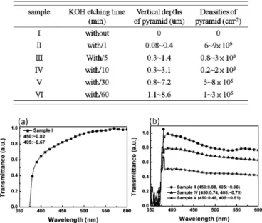
In order to understand the wet-etching process of the RB-LED, we also prepared the GaN substrate samples with various wet-etching times. These samples were also lapped down to about 110 m. Fig. 2 shows the 30 tile-view and cross-sectional (inset) SEM images of the surface morphology on N-face GaN substrate at 80 C in various times of KOH solutions (a) before etching: sample I, (b) 1 min: sample II, (c) 5 min: sample III, (d) 10 min: sample IV, (e) 30 min: sample V and (f) 60 min: sample VI. It was found that pyramidal structure was observed with chemical etching solution of N-face GaN. It was also found that the increased etching time can increase the height of hexagonal pyramids and decrease the density of hexagonal pyramids. These results were summarized in
TABLE I
PYRAMIDRESULTS OFVERTICALDEPTHS ANDDENSITIESWITH
VARIOUSKOH ETCHINGTIMES
Fig. 3. Transmission spectra as a function of wavelength from Ga-face GaN (a) without chemical etching process and (b) with various chemical wet-etch times.
Table I. Previously reported chemical etching solution such as KOH, Sulfuric Acid (H SO ) and PEC was found to selec-tively etch the N-face GaN but not the Ga-face GaN [9], [11]. Li et al. reported the etch reaction under similar conditions
as where KOH is
both a catalyst for the reaction and a solvent for the resulting Ga O [12]. Because the wet-etching process occurs through the negatively charged OH ions, Ga-face GaN is more stable than N-face GaN due to the negatively charged triple dangling bonds at the surface of Ga-polar GaN [9], [12]. In this study, the N-face GaN was exposed at the bottom of the GaN substrate. As a result, hexagonal pyramid will be formed at the bottom of the chip. The etch process constantly reacted by increasing the etching time by exposing more OH ions. It was also found that the etching process ended in six faces of the GaN layer. These results agree well with that reported by Ng et al. [9].
In order to understand the surface texture how to influence the light extraction efficiency, transmission measurements (Perkin Elmer spectrometer, Lambda 40) was performed. Fig. 3 shows the transmission spectra as a function of wavelength from Ga-face GaN substrate after chemical wet-etching process with various etching times. These measured transmittance samples of sample I, II, IV and V are the same as that of SEM measurement, as shown in Fig. 3. The transmission intensity is relative value. Fig. 3(a) is transmittance of GaN substrate without chemical wet-etching process. It was found that the transmittance at 405 nm wavelength is lower than 450 nm wavelength. The transmittance is estimated to reduce by 18.3% from 450 nm to 405 nm because the 405 nm wavelength is close to the GaN bandgap which could possibly suffer from a large absorption than 450 nm wavelength. Fig. 3(b) shows the transmittance of GaN substrate with various chemical wet-etching times. It is notable that the transmittance would strongly depend on the wavelength and the transmittance at
FU et al.: STUDY OF InGaN-BASED LEDs ON A ROUGHENED BACKSIDE GaN SUBSTRATE 1375
Fig. 4. (a) RT EL emission wavelength is measured for these LED samples at a 20-mA current injection. (b) – – characteristics of these fabricated LEDs.
405 nm wavelength is always larger than the transmittance at 450 nm wavelength. After chemical wet-etching process, the transmission value of the 405 nm wavelength of sample II, IV and V is improved by 9.1, 6.8 and 6.3%, compared with 450 nm wavelength. The enhanced ratio decrease with increasing wet-etching time. In other words, the smaller vertical length and higher density of hexagonal pyramids are beneficial to the transmittance at 405 nm wavelength. Therefore, we used the chemical wet-etching processes to compensate for the loss transmittance of 18.3%. Instead, the transmission value of the 405 nm wavelength can be more improved.
Fig. 4(a) shows RT electroluminescence (EL) spectra of these fabricated LEDs with 20 mA current injection. It was found that the EL peak positions of these n-UV and blue LEDs all occurred at 405 nm and 450 nm, respectively. This can be attributed to use of exactly the same epitaxial layer with identical MQW struc-ture of the n-UV and blue LEDs. It was also found that EL in-tensities of the RB-LEDs were larger than the ST-LEDs. This can be attributed to the better light-extraction efficiency for the RB-LEDs. Similar results were also found by C. F. Lin et al. [13] and C. W. Kuo et al. [14]. Fig. 4(b) shows – – charac-teristics of these fabricated LEDs. It was found that 20 mA for-ward voltages of these LEDs were 3.14, 3.16, 3.27 and 3.28 V for the ST-LED I, RB-LED I, ST-LED II and RB-LED II, re-spectively. The slightly larger forward voltage observed from RB-LED is probably related to RB wet-etching-induced dam-ages. It was also found that output power of RB-LED was al-ways larger than that of ST-LED. With 20 mA current injec-tion, it was found that the output powers of these LEDs were 13.2, 25.6, 19.9 and 24.0 mW for the ST-LED I, RB-LED I, ST-LED II and RB-LED II, respectively. It was found that the smaller output power of ST-LED I is attributed to the lower transmittance, compared with ST-LED II. For the RB-LED I and RB-LED II, we can enhance the 20 mA output power by 94% and 21% by using RB structure compared with ST-LED I and ST-LED II, respectively. It is also attributed to the fact that the better light-extraction efficiency for the RB-LEDs. More-over, the different enhanced ratios of RB-LED I and RB-LED II were observed in Fig. 4(b). It is attributed to the fact that the light extraction efficiency of RB-LED I was more improved than that of RB-LED II because of the different transmittance as a function of wavelength by hexagonal pyramids after chemical wet-etching process. For the RB-structure, the output power of RB-LED I is larger by 6.7% than that of the RB-LED II.
IV. CONCLUSION
In summary, nitride-based LEDs with a roughened backside GaN substrate were proposed and fabricated. By chemical
wet-etching process, the hexagonal pyramids can be formed in the N-face GaN substrate. It was found that the increased etching time can increase the height of hexagonal pyramids and decrease the density of hexagonal pyramids. Compared with ST-LED, it was found that we can enhance the 20 mA output power by 94% and 29% from the RB-LED I and RB-LED II, re-spectively. In addition, the output power of RB-LED I is larger by 6.7% than that of the RB-LED II. The larger improvement for n-UV LEDs is attributed to the different transmittance as a function of wavelength by hexagonal pyramids after chemical wet-etching process, compared with blue LEDs.
REFERENCES
[1] T. Mukai, S. Nagahama, M. Sano, T. Yanamoto, D. Morita, T. Mitani, Y. Narukawa, S. Yamamoto, I. Niki, M. Yamada, S. Sonobe, S. Shioji, K. Deguchi, T. Naitou, H. Tamaki, Y. Murazaki, and M. Kameshima, “Recent progress of nitride-based light emitting devices,” Phys. Stat.
Sol. (a), vol. 200, no. 1, pp. 52–57, Oct. 2003.
[2] T. Mukai, M. Yamada, and S. Nakamura, “Characteristics of InGaN-based UV/blue/green/amber/red light-emitting diodes,” Jpn. J. Appl.
Phys., vol. 38, pp. 3976–3981, Jul. 1999.
[3] M. Yamada, T. Mitani, Y. Nakukawa, S. Shioji, I. Niki, S. Sonobe, K. Deguchi, M. Sano, and T. Mukai, “InGaN-based near-ultraviolet and blue-light-emitting diodes with high external quantum efficiency using a patterned sapphire substrate and a mesh electrode,” Jpn. J. Appl.
Phys., vol. 41, pp. L1431–L1433, Dec. 2002.
[4] T. Fujii, Y. Gao, R. Sharma, E. L. Hu, S. P. DenBaars, and S. Naka-mura, “Increase in the extraction efficiency of GaN-based light-emit-ting diodes via surface roughening,” Appl. Phys. Lett., vol. 84, pp. 855–857, Feb. 2004.
[5] C. H. Kuo, C. C. Lin, S. J. Chang, Y. P. Hsu, J. M. Tsai, W. C. Lai, and P. T. Wang, “Nitride-based light-emitting diodes with p-AlInGaN surface layers,” IEEE Electron Device Lett., vol. 52, no. 10, pp. 2346–2349, Oct. 2005.
[6] A. David, T. Fujii, R. Sharma, K. Mcgroody, S. Nakamura, S. P. Den-Baars, E. L. Hu, and C. Weisbuch, “Photonic-crystal GaN light-emit-ting diodes with tailored guided modes distribution,” Appl. Phys. Lett., vol. 88, pp. 061124–061126, Feb. 2006.
[7] E. Matioli, B. Fleury, E. Rangel, T. Melo, E. Hu, J. Speck, and C. Weisbuch, “High extraction efficiency GaN-based photonic-crystal light-emitting diodes: Comparison of extraction lengths between surface and embedded photonic crystals,” Appl. Phys. Express, vol. 3, pp. 032103–032105, Mar. 2010.
[8] C. F. Lin, Z. J. Yang, J. H. Zheng, and J. J. Dai, “Enhanced light output in nitride-based light-emitting diodes by roughening the mesa side-wall,” IEEE Photon. Technol. Lett., vol. 17, no. 10, pp. 2038–2040, Oct. 2005.
[9] H. N. Ng, N. G. Weimann, and A. Chowdhury, “GaN nanotip pyramids formed by anisotropic etching,” J. Appl. Phys., vol. 94, pp. 650–653, Jul. 2003.
[10] C. L. Chao, C. H. Chiu, Y. J. Lee, H. C. Kuo, P. C. Liu, J. D. Tsay, and S. J. Cheng, “Freestanding high quality GaN substrate by associ-ated GaN nanorods self-separassoci-ated hydride vapor-phase epitaxy,” Appl.
Phys. Lett., vol. 95, pp. 051905–051907, Aug. 2009.
[11] Y. Gao, M. D. Craven, J. S. Speck, S. P. DenBaars, and E. L. Hu, “Dis-location- and crystallographic-dependent photoelectrochemical wet etching of gallium nitride,” Appl. Phys. Lett., vol. 84, pp. 3322–3324, Apr. 2004.
[12] D. Li, M. Sumiya, S. Fuke, D. Yang, D. Que, Y. Suzuki, and Y. Fukuda, “Selective etching of GaN polar surface in potassium hydroxide solu-tion studied by X-ray photoelectron spectroscopy,” J. Appl. Phys., vol. 90, pp. 4219–4223, Oct. 2001.
[13] C. F. Lin, C. M. Lin, K. T. Chen, W. C. Huang, M. S. Lin, J. J. Dai, R. H. Jiang, Y. C. Huang, and C. Y. Chang, “Blue light-emitting diodes with a roughened backside fabricated by wet etching,” Appl. Phys. Lett., vol. 95, pp. 201102–201104, Nov. 2009.
[14] C. W. Kuo, Y. C. Lee, Y. K. Fu, C. H. Tsai, M. L. Wu, G. C. Chi, C. H. Kuo, and C. J. Tun, “Optical simulation and fabrication of niteide-based LEDs with the inverted pyramid sidewalls,” IEEE J. Sel. Topics