RMOlB-5
18-26 GHz Low-Noise
Amplifiers Using 130-
and
90-nm
Bulk
CMOS Technologies
Shih-Chieh Shin, Szu-Fan Lai, Kun-You Lin, Ming-Da Tsai, Huei Wang, Chih-Sheng Chang*, and
Yung-Chih Tsai*
Dept.
of
Electrical Engineering and Graduate Institute of Communication Engineering,
National Taiwan University, Taipei,
106, Taiwan, R.O.C.
d
"Taiwan Semiconductor Manufacturing Company, Hsinchu City,
300,
Taiwan, R.O.C.
Abstruct
-
Two 18-26 GHz CMOS low-noise amplifiers using 130- and 90-nm bulk CMOS technologies are describedin this paper. The thin-film microstrip (TFMS) LNA using 130-nm CMOS process demonstrates a peak gain of 12.9 dB at 21 GHz with 3-dB bandwidth of 18.6 to 26.3 GHz and a noise figure (NF) of better than 5.4 dB between 20 and 26 GHz. The coplanar waveguide (CPW) amplifier fabricated by 90-nm CMOS process presents a peak gain of 16.2 dB with a 3-dB bandwidth of 18 to 26 GHz, and a NF of better than 4 dB from 18 to 26 GHz.
lndex Terms
-
CMOS, low-noise amplifier, thin-film microstrip line, coplanar waveguide.I. INTRODUCTION
The rapidly growing demand for larger bandwidth
motivates RF circuits to move toward higher frequencies. At frequencies above 20 GHz, GaAs-based HEMT and
HBT MMICs occupied most of the applications. Recent works have illustrated the rapid development of CMOS
devices to have the potential of building RF circuits at frequencies above 20 GHz. Although LNAs using SOT CMOS process demonstrated excellent performances [ 11,
the standard bulk CMOS process is still attractive because
of cost consideration. There were some reports of bulk CMOS LNAs designed for frequencies above 20 GHz, and most of them were designed using the lumped elements [2]-[3]. Several high-frequency CMOS amplifiers were designed using transmission lines to reduce the lossy substrate effect 14]-[7]. A 20- and a 40-GWz TFMS amplifiers fabricated by 90-nm CMOS technology were reported with good agreement between the simulated and measured results [4]. A 0.18-pin CMOS distributed amplifier designed using TFMS demonstrates a 4-dB gain and a 39-GHz bandwidth [ 5 ] . A 27-GHz TFMS tuned amplifier consists of three-stage cascode cells demonstrated 17-dB gain [6]. By adopting coplanar waveguide, a 60-GHz LNA cascaded by 3-stage cascode
cells was presented [7]. It is observed that the CMOS
circuits using either TFMS or CPW demonstrated good
0-7803-8983-2/05/$20.00 0 2005 IEEE
performance in high frequency range.
In
this paper, we present aTFMS
and a CPW LNAs fabricated using TSMC 130- and 90-nm bulk CMOS technologies, respectively. The TFMS amplifier was implemented with a very compact chip size since the thin- film spiral inductors can be utilized in this design. The CPW LNA fabricated by 90-nm technology demonstrates the better gain and noise performances. Table Isummarizes the performances of the previously reported LNAs designed for frequencies around 20 GHz. Both of
these amplifiers present the comparable gain of GaAs- based 'pHEMT
LNA
[SI, with slightly higher noise performance for our 90-nm CPW CMOS design.11.90- AND 130-NM CMOS CHARACTERISTICS AND PROCESSES
The TFMS and CPW amplifiers are fabricated by 130- nm one-poly-eight-metal (1PXM) and 90-nm one-poly- nine-metal ( 1WM) processes, respectively. The 130-nm process has a n f r of 85 GHz and anf,, of 90 GHz while
the 90-nm process demonstrates an f , of 160 GHz and an
f,,,
of 142 GHz. Both of these two processes provide the top metallization of 2-pm thickness for low lossinterconnection.
MIM
capacitors with 1 - and 1.5-fF/pmz
unit capacitance are also provided in 130- and 90-nmprocesses, respectively.
111. THIN-FILM MICROSTRIP LINE AND COPLANAR
WAVEGUIDE TN CMOS PROCESS
Figure I shows the structures of the TFMS and CPW. The TFMS consists of the top metal (M8) as the signal strip and bottom metal
(MI)
as ground plane in the 130- nm CMOS process. The TFMS has the advantage of the ground plane shielding to isolate the conductive substrate. The matching elements of transmission lines can be replaced by thin-film spiral inductors or meandering lines in a very small area to reduce the circuit size. However,47
TABLE
ICOMPARISON WITH PREVlOUSLY REPORTED LNAS FOR FREQUENCIES AROUND 20 GHZ.
3 stages, CGRF+CS+CS
Bandwidth Gain Chip Size
I
( G W1
(d3)I
NF(dB)1
(mm2) Process ['I I I I 1 ~O-IUIICMOS1
0.1 8-pm CMOS1
-1
1
6;;yz)1
;m:
124-
26 GHr) 0'735 0.18-win CMOS 22-
25 0. t 8-pm CMOS 23-
28 12 86 j23-
24 G H r ) 6.9 - a 17-28 6 j 1 7 - 2 0 G H z ) 5 - 7 0.56 1.6-1.9 o 9 0.15-pm1
TnGaPflnCaAs IIEMT 2 3 - 3 0I
14S l ( 1 9 - 3 3 C l h )I
I
90-nmCMOS1
18-26 1 1 6 . 21(18-26GHz,I
2.5-
4 0.8 I I I I* CS: common source. CGRF. common I pate resistive feedthrough.
1 . Test pads are not included.
the characteristic impedance of the TFMS is dominated by the signal strip width, high-impedance lines are difficult to be implemented due to the thin SiO, layer of 5.5 pm.
Passivation Passivation
la) (b)
Fig. 1. The structures of the (a) TFMS, and (b) CPW on bulk
CMOS process.
CPW is constructed by one signal strip and two ground metals on the same plane as shown in Fig. l(b), and the signal and ground metals are implemented by the top metal. The characteristic impedance of the CPW is defined by the signal metal width and the gap size between signal and ground metal, thus it is more flexible to realize different impedances of CPWs. To suppress the unwanted odd-mode
signal,
the two ground
planesof
CPW should be forced to be equal potential. It is easy to
implement by using the second metal to connect the two ground planes in CMOS process. The conductive substrate effect is reduced by using CPW, however it is
not fully removed. Thus the substrate effect of CPW still needs to be considered. The TFMS can be meandered in very compact size, but not for CPW because CPW needs the well-defined ground planes.
24 54 - 54 10 37.5 - 16.8 26 4 3 stages,
I
cs+cs+cs
I
L31:
3 stages, L.8I
CStCS+CSI
'31I
I I I , , 2I
2stages,I
ThisI
CStCS, TFMS Work1
2stages,I
ThisI
cs+cs. CPW workIV. CMOS LNA USING TFMS
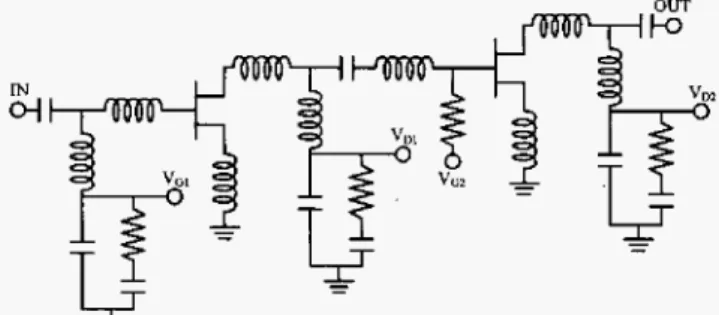
This amplifier fabricated by 130-nm lP8M CMOS
process is a two-stage single-ended design. The transistors in each stage are 18 fingers with a total gate periphery of 36 pm. Figure 2 shows the schematic, and
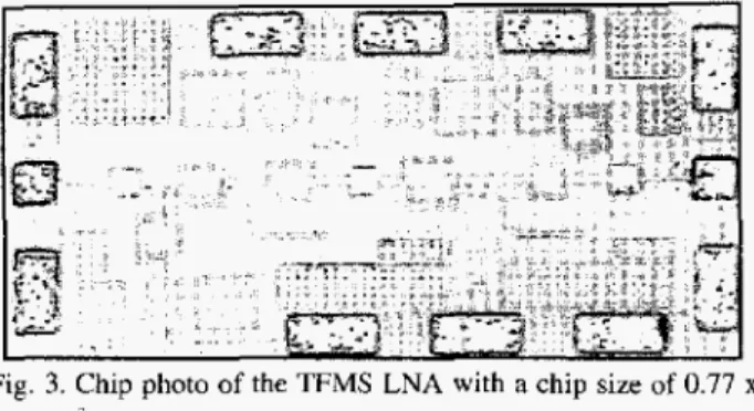
the corresponding chip photo is shown in Fig. 3. The matching networks consist of series and shunt inductors to transform the impedance to 50 $2. In order to minimize the circuit size, the thin-film spiral inductors are used as the matching elements. The source inductors implemented by the transmission lines are utilized in both
stages for stability concern. All of the passive elements
include thin-film
spiral inductors,
capacitors and transmission lines are simulated using the EM simulator Sonnet. The chip size is 0.77 x 0.4mm'.
'
-
Fig. 2. Schematic of the TFMS LNA.
Fig. 3. Chip photo of the TFMS LNA with a chip size of 0.77 x
0.4 nun'-.
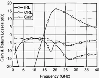
The measured small-signal gain and retum losses are shown in Fig. 4 under 1.2 V with a total power consumption of 16.8 mW. The measured peak gain is 12.9 dB at 21 GHz with the gain higher than 10 dB from
18.6 to 26.3 GHz. The input return loss is better than 10
dB between 18.6 and 23.8 GHz, and the output return loss is better than 10 dB above 19.6 GHz. Figure
5
shows the measured noise figure, and this amplifier has a noise figure of better than 5.4 dB from 20 to 26 GHz.V. CMOS LNA USING CPW
This amplifier which is fabricated in the 90-nm 1P9M
CMOS process employs a two-stage cascaded common- source structure. Both transistors in this circuit are 16
fingers with a total gate width of 64 pm. Figure 6 shows the schematic, and the corresponding chip photo is shown in Fig. 7. The input and output are matched to 50 by series transmission lines as well as short stubs. The technique of source degeneration is utilized in both stages for stability concern. The second stage employs a parallel resistive feedback, which leads to a broadband response. The matching elements of CPWs are meandered to achieve a smaller chip size of 0.98 x 0.82 mm2.
-
-
Fig. 6 . Schematic of the CPW LNA.
--
0 5 IO 15 20 25 30 35 40
Frequency (GHz)
Fig. 4. Measured small-signal gain and retum losses of the TFMS LNA.
Fig. 7. Chip photo of the CPW LNA with a chip size of 0.98 x
0.82 mm'.
Frequency (GHz) Fig. 5. Measured noise figure of the TFMS LNA.
The measured small-signal gain and retum losses are shown in Fig. 8 under 1.2 V with a total power consumption of 26.4 mW. The measured peak gain is 16.2 dB at 20.5 GHz with the 3-dB bandwidth of 8
GHz
from 18 to 26 GHz. Figure 9 shows the measured noise figure, and this amplifier has a noise figure of better than 4
dB in the entire 3-dB bandwidth. At 22.5 GHz, the noise
figure achieves a minimum of 2.5 dB which is the lowest
NF among the reported MMIC LNAs using bulk
CMOS
processes in this frequency.
0 5 10 .I5 20 25 30 35 40
Frequency (GHz)
Fig. 8. Measured small-signal gain and return losses of the CPW LNA.
Frequency (GHz) Fig. 9. Measured noise figure of the CPW LNA.
VI.
CONCLUSIONThe 130- and 90-nm CMOS LNAs were developed
using
TFMS
andCPW,
respectively. These two amplifiers demonstrate wideband characteristics and good gain and noise performance. Both of the TFMS and CPWcan reduce the effect of lossy substrate, thus they are the better alternatives than the lumped elements in millimeter- wave CMOS circuit designs.
ACKNOWLEDGEMENT
This work is supported in part by NTU-TSMC Joint- Development Project and National Science Council of
Taiwan R.O.C. (Projects NSC 93-2219-E-002-016, NSC 93-2219-E-002-024, NSC 93-2213-E-002-033, and NSC 93-2752-E-002-002-PAE).
REFERENCES
Frank Ellinger, “26-42 GHz SO1 CMOS low noise amplifier, “ JEEE J. Solid-State Circuits, vol. 39, no. 3, pp.
Xian Guan, and Ali Hajimiri, “A 24-GHz CMOS front end,” IEEE J. Solid-State Circuits, vol. 39, no. 2, pp. 368- 373, Feb. 2004.
K,-W. Yu, Y.-L. Lu, D.-C. Chang, Victor Liang, and M. Frank Chang, “K-Band low-noise amplifiers using 0.18 ~ I I
CMOS technology, ” IEEE Microwave And Wireless
Components Ledf., vol. 14, no. 3, pp. 106-108, March 2004.
A. Masud, H. Zirath, M. Femdahl, and H.-0. Vickes, “90 nm CMOS MMlC amplifier,” 2004 R F K symp. Dig., 2004, pp. 97 1-974.
H. Shigematsu, M. Sato, T. Hirose, F. Brewer, and M.
Rodwell, “40Gbis CMOS distributed amplifier for fiber- optic communication systems,” ISSCC Dig. Tech. Papers,
pp. 476-477, Feb. 2004.
H. Shigematsu, T. Hirose, F. Brewer, and M. Rodwell,
“CMOS circuit design for millimeter-wave applications,”
2004RFICsymp. Dig., 2004, pp. 123-126.
C. H. Doan, S. Emami, A. M. Niknejad, and R. W.
Brodersen, “Design of CMOS for 60GHz applications,”
ISSCC Dig. Tech. Papers, pp. 440-44 1, Feb. 2004.
Y. Mimino, M. Hirata, K. Nakamura, K. Sakamoto, Y.
Aoki, and S. Kuroda, “High gain-density U-band P-HEMT
LNA MMIC for LMDS and satellite communication,” in
Proc. IEEE MTT-S h i . Microwave Symp., vol. 1 , June 522-528, March 2004
2000, pp. 17-20.