The Design of Low-Power CIFF Structure Second-Order
Sigma-Delta Modulator
Pin-Han Su and Herming Chiueh Department of Electrical Engineering
National Chiao Tung University, Hsinchu 300, TAIWAN e-mail: supin@soclab.org, chiueh@ieee.org
Abstract — This paper presents the design and
implementation of a low power sigma-delta modulator (SDM) with a standard 0.18-µm CMOS technology. A
current optimization technique is utilized in proposed design to reduce the power of operational trans-conductance amplifier(OTA). Using a chain of Integrators with weighted feed-forward summation (CIFF) structure and optimized single-stage class-A OTA with positive feedback to minimize the power consumption, the second-order SDM achieves a SNR of 64dB that be able to process the signal form DC to 16 KHz. The power consumption is only 18.1 uW from a 1-V supply.
I. INTRODUCTION
With the scaling down of modern VLSI technologies, more complicate digital circuits have been implemented with a higher clock rate and lower supply voltage, which introduces more constraints for the analog circuits. Therefore, the design of low-voltage, low-power analog circuitries has become more important. Because of powered by batteries, the supply voltage is often limited, and the life time of the battery is of great importance for these devices, and all these factors address the requirements of low-power system building blocks. However, the decreased supply voltage restricts the signal swing in circuits and brings difficulties for analog circuit design. In low-voltage environments, the transistor characteristics degrade and some circuit techniques can no longer be used, thus the low-voltage design different from the traditional circuit design technique.
With the rapid growing of portable devices, a battery-based operation system is highly desired by various emerging applications, such as mp3 players, radio-frequency identification (RFID), and portable biomedical applications (such as digital hearing aid instrument.) In these devices, the analog-to-digital converters (ADCs) are important building blocks, because it is necessary to transfer nature analog signal to digital code.
Among different ADC topologies, the Sigma-Delta ADCs efficiently trade speed for accuracy, providing an efficient
way to implement high-resolution ADCs without stringent matching requirements compared to other types of ADCs (ex: flash ADC, pipeline ADC) in audio band applications. By over-sampling and noise shaping, the sigma-delta ADCs transfer most of the signal processing tasks to the digital domain. Therefore, for high-resolution ADCs, the sigma-delta ADCs are more power-effective and robust compared to other architectures.
There are many state-of-the-art low-power researches: In [2], a switched-op technique combined with a dc level shift has been proven to allow proper operation under low VDD conditions (0.7V), thus lower the power consumption; A new fully differential CMOS class AB Operational Amplifier with a charge-pump is proposed [3]; And a load-compensated OTA with rail-to- rail output swing and gain enhancement is used in a 90nm technology [4]; And in [5], a 0.6V folded-cascode OTA topology is used in a 2-2 cascade delta-sigma ADC design with a resistor-based sampling technique. In [6], a switched-current SDM is used for a bio-acquisition Microsystems with 0.8V power supply. And a digital hearing aid chip is proposed [7]; In [8], a ADC is designed and optimized for a CMOS image sensor; Finally [9], a 4th order
SDM is presented with a single stage class A OTA and positive feedback. All of them focus on reducing the power consumption for audio-band applications. Among above researches, some of them choose adaptive OTA topology to reduce power and the others try to use extra technique or CMOS technology to lower power supply, thus lower power consumption.
In this paper, a SDM topology for low-power application and a suitable OTA architecture is used. Then a current optimization method is proposed to reduce the power consumption using a standard 0.18um CMOS technology. The target resolution is at least 10 bits while the maximum signal bandwidth is 16KHz.
This paper is organized as follows: The system consideration is described in section II. Then, the proposed SDM system and circuit is described in section III. Finally, the simulation results and conclusion is will be given out.
II. SYSTEM CONSIDERATIONS OF LOW POWER SDM
Architecture selection
The most general single stage topology in the SDM design is the CIFB architecture, and the output signal of the integrators are the functions of input signal x(z), so if we want to have a full scale input signal x(z), than there will be a large output swing at the output of the integrator, hence the power of the OPAMP will increased .
Because the nature restriction of the CIFB architecture, another architecture is chosen for low-power design [1], the CIFF architecture have some advantages, and it is shown in Figure 1:
Figure 1 A second-order SDM with CIFF structure The output signals of two integrators in CIFF structure are not contain the input signal x(z),which means that this loop filter process E(z) only, thus the output swing requirements of the loop filter will decrease, it means that the slew-rate requirement is not critical when we design the OTA in loop filter [3], so it is more suitable for low-power applications.
Coefficient Selection
In a general structure of CIFF sigma-delta modulator, it contain 5 coefficients: two integrator gain (a1,a2) and three summation factor(b0,b1,b2). And it will contain fourteen capacitors, shown at Figure 2:
Figure 2 Circuit Level second-order CIFF SDM From the Delta-Sigma Toolbox, given an order=2, OSR=64, the noise transfer function NTF(z) that have SNR(max):
(
)
4415 . 0 225 . 1 1 ) ( 2 2 + − − = z z z Z NTFAfter deciding the transfer function of the SDM, we must deiced which combination of (a1,a2,b1,b2,b3) we will use. Because our target is to achieve low-power, and the most important feature of a low power SDM is that the signal swing at the loop filter output is small than others.
When the coefficient a1 is larger, the output swing of the loop filter is larger, then the power consumption is larger of
the whole modulator; therefore, if we want to have a smaller signal swing, a1 must be minimized. However, if a1 is too small, the stability of the SDM will be degraded because the signal will overload, and the SNR will decrease, so we must make a trade-off between the coefficients.
In this work, we choose a1=0.25 and b1=0.3 combined above requirement, capacitor matching and the signal scaling issues.
Under the coefficients, the modified NTF becomes:
(
)
5 . 0 25 . 1 1 ) ( 2 2 ' + − − = z z z Z NTF .The slightly change of the NTF pole will not degrade the SNR significantly.
III. CIRCUIT IMPLEMENTATION OF PROPOSED SDM
The low-power single stage class-A OTA
The OTA in loop filter is the analog block which consume the most power, and it also dominant the performance of the modulator, so it is the most critical building block that we must design it seriously.
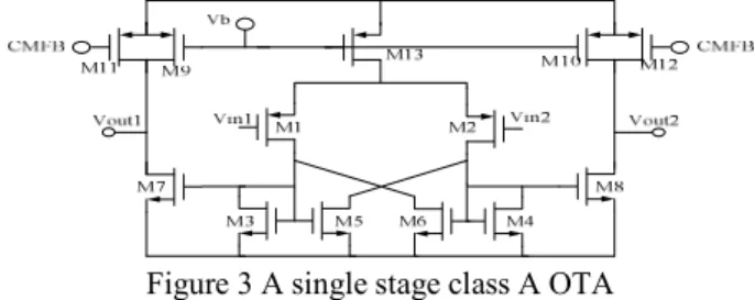
In [4], a single stage OTA must be used because it doesn’t have to waste extra current in driving the compensated capacitance. Although the class-AB OTA is the most widely used OTA architecture when designing a low power SDM, it requires extra paths to drive the transistor of output stage; Therefore, a single-stage class-A Amplifier with positive feedback to increase its gain [9] is used in this design, as shown in Figure 3:
Figure 3 A single stage class A OTA
When the loop filter is at integration period, the settling behavior of the OTA can be derived as the figure. A slewing is happened when a large output change of the loop filter. When the differential input voltage less than
2
V
OV , the OTA enters linear settling region.With a 2MHz clock, the integration period is 250ns, it is to say that Tsr + Tlinear = 250ns, thus the slewing behavior is related to the current of output path:
SR load out T V C I = ⋅∆ 2
For a load capacitance of 2.5pf and a v=0.5, we can derive that: SR out T x I 13 10 49 . 4 − =
The speed of the OTA settling is depend on its time
constant, therefore , the unit gain bandwidth, therefore the input path current of the OTA, we set the linear settling period is larger than 10 time constant , thus the settling error is lower than 85dB.Therefore,
T
linear≥
10
τ
so the unit-gainbandwidth: linear T GBW 1.59 21 = = πτ ,
And the unit-gain bandwidth:
α π − = 1 2 1 B C g GBW L m Thus,
(
)
B C V V T I GS t load t linear in α π⋅ − − = 1.59 2 1For
V
OV=
0
.
1
v
,
α
=
0
.
25
,
B
=
4
, we can derived that :linear in T x I 13 10 78 . 0 − =
From above equations, we can derive the total current consumption of the OTA as:
(
)
SR SR out in total T x T x I I I − + = + = − − 250 10 6 . 1 10 9 . 8 2 13 13The minimum current occurs at Tsr=160 to 170ns. However, when Tsr=170ns is selected, we can calculate that:
uA T x I linear in 1.3 10 78 . 0 13 = = − uA T x I SR out 2.56 10 49 . 4 13 = = −
That the B of the OTA is about 3, which depart from our assumption, so we must decrease the Tsr so that the B is close to 4. Here we select Tsr=130ns. Therefore,
uA T x I SR out 3.45 10 49 . 4 13 = = −
Therefore, the power of the first OTA can be reduced. The second OTA is designed like the first one, while its specifications can be scaled down as the input signal has been processed by one-order noise shaping.
Dynamic CMFB
Because of the differential architecture of the OTA, we must have a CMFB circuit, thus a dynamic CMFB circuit is used because it is the most power-efficient, Vcmo is set to 0.5V. Only the switches connect to CMFB use CMOS switch, other switches is PMOS switch only.
Figure 4 Dynamic CMFB
1-Bit Quantizer & Clock Generator
The 1-bit quantizer, shown in Figure 5, is realized with a comparator and a SR latch. The comparator is a dynamic comparator to lower average power consumption. When the
CLK signal is high, the comparator compares the two input voltage, then the comparison result is followed by the SR latch behind the comparator.
Figure 5 A low power 1-Bit Quantizer
The clock generator in this SDM is designed on-chip, an external clock input signal is buffered and then two non-overlapping clock signals are generated. To avoid the signal dependent charge injection, two delayed clocks, i.e., C1d and C2d, are also generated.
IV. EXPERIMENTAL RESULTS
The proposed SDM, as shown in Figure 6, has been implemented using a 0.18um CMOS technology. The simulation results show the performance of the proposed class-A OTA. The DC gain is around 61dB.The unit gain bandwidth is about 22MHz, and the slew-rate is 3.8V/us for a 2.5pf load while the phase margin is 57°. The output swing is from 100mV to 900mV.
Figure 6 A low-power second-order CIFF SDM circuit Table 1 Performance Summary of the Class A OTA
Specification Result Gain 61.3dB Unit Gain Bandwidth 22.2MHz
Phase Margin 57°
Slew Rate 3.8 V/us Settling Time Constant 12ns
Output Swing 800mV Power Dissipation 10.14uW
Figure 7 shows the 8192-point FFT output spectrum of the proposed SDM, the input signal frequency is 4.4KHz with a -3dB full scale Amplitude. It shows that the SNR is about 64.3dB and the SNDR is 58dB.
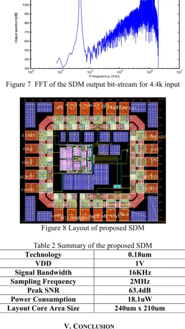
Figure 8 is the chip photograph of the SDM, the area is 840umx760um with ESD pad, while the active area is only 240umx210um.The summary of the simulated results of the modulator is shown in Table 2.
102 103 104 105 106 107 30 40 50 60 70 80 90 100 110 120 Frequency [Hz] O ut put s pe ct rum [d B ]
Figure 7 FFT of the SDM output bit-stream for 4.4k input
Figure 8 Layout of proposed SDM Table 2 Summary of the proposed SDM
Technology 0.18um VDD 1V Signal Bandwidth 16KHz
Sampling Frequency 2MHz Peak SNR 63.4dB Power Consumption 18.1uW Layout Core Area Size 240um x 210um
V. CONCLUSION
A low-power second-order SDM with CIFF structure and a single stage class-A positive feedback OTA operating at 1v supply has been presented. By using 0.18um CMOS technology, this modulator achieves SNR of 63.4dB with 16KHz bandwidth, and it is suitable for battery-based audio portable electric devices. By using a CIFF structure and a low-power class-A OTA with positive feedback, the SDM is done with optimization procedure to power consumption. The simulation results show that the power consumption is 18.1uW. It is the lowest compared to references [2-9].
Acknowledgment
The authors would like to thank the National Chip implementation Center (CIC) for the support during the project and the TSMC for providing the 0.18um CMOS technology. This research is supported by National Science Council, Taiwan, the contract numbers are: NSC97-2220-E-009-005, NSC97-2220-E-009-042, NSC98-2220-E-009-002.
REFERENCES
[1] J.Silva, U.Moon, J.Steensgaard and G.C. Temes, “Wideband low-distortion delta-sigma ADC topology,” Electronics Letters, June 2001.
[2] J.Sauerbrey, T.Tille, D. Schmitt-Landsiedel, R.Thewes, “A 0.7V MOSFET-Only Switched-Opamp Modulator in Standard Digital CMOS Technology,” IEEE Journal of Solid-State Circuits,” Vol. 37, No. 12,Dec 2002. [3] Y.Hu , Z.Lu , M.Sawan, “A Low-Voltage 38uW
sigma-delta Modulator Dedicated to Wireless Signal Recording Applications,” ISCAS 2003.
[4] L.Yao, Michael S.J.Steyaert, W.Sansen, “A 1v 140uW 88dB Audio Sigma-Delta Modulator in 90nm CMOS,” IEEE Journal of Solid-State Circuits, Vol. 39, No. 11, Nov 2004.
[5] G.Ahn, M.E.Brown, N.Ozaki, H.Yiura, K.Yamamura, K.Hamashita, K.Takasuka, G.C.Temes, “A 0.6V 82dB Delta-Sigma Audio ADC Usgin Switched-RC Integrators,” IEEE Journal of Solid-State Circuits, Vol.40 , No. 12, Dec 2005.
[6] S.Lee, C.Cheng, “A Low-Voltage and Low-Power Adaptive Switched Current Sigma-Delta ADC for Bio-Acquisition Microsystems,” IEEE Transactions on Circuits and Systems-Regular Papers, Vol. 53, No.12, Dec 2006.
[7] S.Kim, J.Lee, S.Song, H.Yoo, “An Energy-Efficient Analog Front-End Circuit for a Sub-1V Digital Hearing Aid Chip,” IEEE Journal of Solid-State Circuits, Vol. 41, No.4, April 2006.
[8] A.Mahmoodi , D.Joseph, “Optimization of Delta-Sigma ADC for Column-Level Data Conversion in CMOS Image Sensors,” IEEE IMATC, May 2007.
[9] J.Roh, S.Byun, Y.Choi, H.Roh, Y.Kim, J.Kwon, “A 0.9V 60uW 1 bit Fourth-Order Delta-Sigma Modulator with 83dB Dynamic Range,” IEEE Journal of Solid-State Circuits, Vol.43, No.2, Feb 2008.
[10] Richard Schreier, G.C Temes, ”Understanding Delta-Sigma Data Converters,” Institute of Electrical and Electronics Engineers Inc, 2005.
[11] Shahiar Rabii, Bruce A.Wooley, The Design of
Low-Voltage, Low-Power Sigma-Delta Modulators, Kluwer
Academic Publishers 1999.
[12] Roubik Gregorian, Introduction to CMOS OP-AMPS
and Comparators, John Wiley & Sons, 1999.