國 立 交 通 大 學
電子工程學系 電子研究所碩士班
碩 士 論 文
1.25 億位元/每秒四分之一時脈與資料回復電路
設計與實現
Design and Realization of a 1.25Gb/s Quarter
Rate Clock and Data Recovery Circuit
研 究 生:林建華
指導教授:羅正忠 博士
1.25 億位元/每秒四分之一時脈與資料回復電路
設計與實現
Design and Realization of a 1.25Gb/s Quarter
Rate Clock and Data Recovery Circuit
研 究 生:林建華 Student:Jian-Hua Lin
指導教授: 羅正忠 博士 Advisor:Dr. Zheng-Zhong Luo
國 立 交 通 大 學
電子工程學系 電子研究所碩士班
碩 士 論 文
A Thesis
Submitted to Department of Electronics Engineering & Institute of Electronics College of Electrical and Computer Engineering
National Chiao-Tung University in partial Fulfillment of the Requirements
for the Degree of Master in
Electronics Engineering July 2006
Hsinchu, Taiwan, Republic of China
1.25 億位元/每秒四分之一時脈與資料回復電路
設計與實現
研究生:林建華
指導教授:羅正忠 博士
國立交通大學
電子工程學系 電子研究所碩士班
摘要
隨著資料在高速傳輸的需求日益增加,其資料的正確性和時脈的
穩定性在類比與數位電路系統中更顯重要,包含通訊系統、有線與無
線網路、頻率調變訊號的解調、電腦與周邊設備的連結及各網域間的
連線等,我們已經利用光纖媒介來達到高頻和低損耗的傳輸[1],但
在接收端更需小心的確保資料流並沒有因雜訊的累加而放大了誤
差。資料與時脈回復器在此即扮演了關鍵角色,將時脈從接收到的資
料中取出並重新取樣被污染的資料。
本論文的主題在完成一個雙迴路的 1.25Gb/s 資料與時脈回復
I器,並且完全使用互補式金氧半製程來實現以達到低功率、高度整合
的優點,為達到未來系統晶片強調的超低功率,我們更把時脈的頻率
降低且在不影響速度的前提下達到成效。另一方面,省卻除頻器的架
構改採解多路傳輸資料的方式。論文分為四章,第一章為簡介,第二
章介紹光纖傳輸與資料和時脈回復器的背景,第三章為本論文設計的
重點與模擬結果,第四章是比較其他篇論文, 最後總結整個設計以及
針對未來設計提出建議。
IIDesign and Realization of a 1.25Gb/s Quarter
Rate Clock and Data Recovery Circuit
Student:Jian-Hua
Lin
Advisors:Dr. Zheng-Zhong Luo
Department of Electronics Engineering & Institute of Electronics
National Chiao Tung University
Abstract
With the increasing demand of high speed transport of data, it is more important
that the accuracy of data and the stability of clock in analog and digital systems.
Fibers provide much greater bandwidths and lower losses in many areas, inclusive of
communication systems, wireline and wireless network, demodulation of
frequency-modulated signals, many high speed links between computers and other
peripheral, and the connection of such LAN/WAN, etc. But we must be more careful
not to amplify the error by the jitter accumulation. Data and clock recovery plays a
critical part here to extract the real clock from data and retime the dirty bits.
The goal of this thesis is to use standard CMOS process to realize a 1.25Gb/s
dual-loop data and clock recovery. To attain the aim of low power what we put
emphasis on SOC, deep sub-micron CMOS technology is now being considered
because of that advantages such as low power, highly integrated capacity. On the
other hand, it does not require a frequency divider and we utilize demultiplexer to
retime data. The paper could be divided into four chapters. Chapter 1 is the
introduction. Chapter 2 presents the background of fiber transport and data and clock
recovery. Chapter 3 is the purpose of mainly architecture and the simulation. Chapter
4 is the comparison with other papers. Finally, I summarize all design and give it
some suggestion for future work.
誌謝
首先我要說的是,進入國立交通大學的電子研究所對求學生涯可
以說是完全不一樣的轉變,平日專業書籍的閱讀和課題的演練,乃至
實地的電路設計每每讓返家的時間不定,但也因此訓練出獨立思考的
能力和諸多解決問題的辦法。
各個實驗室互相幫忙的風氣也是學校和學生進步的關鍵,所以在
這首先感謝黃俊達教授實驗室的孝恩、陳巍仁教授實驗室的高麗菜與
188、黃宇中教授實驗室的志賢、清華大學電機所的小龜龜與逸聖、
陳宏明教授實驗室的嘉倫,當然,最重要的是敝實驗室的倪董、國龜、
老龜、愛玉、致維、忠樂以及明衡學長、宗翰學長和許多學弟,最後,
還有我的指導教授羅正忠老師,課堂充實的內容和課後每週定期關心
學生們的進度,都是我在完成論文的過程中由衷感謝的。
VContents
Abstract (Chinese)...I Abstract (English)...III Acknowledgement...V Contents...VI Table Captions...VIII Figure Captions...IXChapter 1 Introduction
1-1 Backgrounds………...1 1-2 Transmitter………...2 1-3 Receiver……….3 1-4 NRZ and RZ………..41-5 Organization of the thesis………5
Chapter 2 Clock and Data Recovery Architecture
2-1 Principle of Operation...62-2 Phase Detector…………...7
2-2-1Operation Speed...9
2-3 Frequency Detector………...12
2-3-1Design of Frequency Detector………...14
2-4 Voltage Controlled Oscillator...20
2-4-1 Ring Oscillator...24
2-5 Loop Filter...26
2-6 Loop Performance Analysis………...28
2-6-1 Damping Factor……….29
Chapter 3 A 1.25Gb/s Quarter Rate Clock and Data Recovery Design
3-1 Introduction...313-2 Circuit Description...31
3-2-1 Phase Detector...31
3-2-2 Frequency Detector...35
3-2-3 Voltage Controlled Oscillator………...………37
3-2-3-1 Duty-Cycle Corrector………39 3-2-3-2 Linearization Circuit……….41 3-2-4 Charge Pump……….…………44 3-2-4-1 Charge Pump 1………...44 3-2-4-2 Charge Pump 2………...46 3-2-5 Demultiplexer……….46
3-3 System Simulation Result………...51
Chapter 4 Conclusions and Future Work
4-1 Conclusions...564-2 Future Work...56
Reference
...58Table Captions
Table 2-1 Comparison with Full-rate/Half-rate and Quarter-rate CDR. Table 2-2 Comparison between LC-tank oscillator and ring oscillator [21] Table 4-1 CDR performance summary
Figure Captions
Fig. 1-1 Simple OC system. Fig. 1-2 Fiber-optic transmitter. Fig. 1-3 Fiber-optic receiver. Fig. 1-4 NRZ and RZ data formats. Fig. 1-5 PSD of NRZ and RZ data.
Fig. 2-1 Conventional simple one loop CDR. Fig. 2-2 Bang-bang PD characteristic.
Fig. 2-3 CDR circuit using Alexander PD.
Fig. 2-4 Full-rate/Half-rate and Quarter-rate data and clock.
Fig. 2-5 (a) Architecture of the phase detector, (b) timing chart, and (c) modified. Fig. 2-6 CDR architecture using reference clock.
Fig. 2-7 Proposed CDR architecture using two loops. Fig. 2-8 Quadricorrelator.
Fig. 2-9 (a) Digital version of Quadricorrelator for (b) fast clock and (c) slow clock. Fig. 2-10 (a) Schematic of the FD, and its timing chart of (b) fast data and (c) slow data. Fig. 2-11 State representation.
Fig. 2-12 Combinational logic gate. Fig. 2-13 Feedback system.
Fig. 2-14 Model of a VCO.
Fig. 2-15 Characteristic of a VCO. Fig. 2-16 Ring oscillator using inverters. Fig. 2-17 Problem of insufficient gain.
Fig. 2-18 Delay cell using differential common-source stage.
Fig. 2-19 Second-order loop filter.
Fig. 2-20 Loop response of third-order CDR. Fig. 2-21 CDR basic model without FD.
Fig. 2-22 The transient response of CDR to a frequency step. Fig. 2-23 Frequency response of the CDR.
Fig. 3-1 Proposed architecture of the phase detector. Fig. 3-2 Timing chart of the proposed PD waveform. Fig. 3-3 Schematic of TSPC DFF.
Fig. 3-4 Schematic of XOR gate.
Fig. 3-5 Proposed architecture of the frequency detector. Fig. 3-6 Schematic of DETFF gate.
Fig. 3-7 Schematic of four stages VCO and its delay cell. Fig. 3-8 Proposed VCO with control region.
Fig. 3-9 (a) Schematic of feed forward duty-cycle corrector and (b) its timing diagram. Fig. 3-10 (a) Schematic of linearization circuit and (b) its Vin/Vo curve.
Fig. 3-11 The transfer curve of VCO (a) without linearization circuit and (b) with it. Fig. 3-12 Schematic of charge pump 1.
Fig. 3-13 (a) Charge sharing phenomenon and (b) eliminated by additional devices. Fig. 3-14 (a) Original current reuse charge pump and (b) its modify.
Fig. 3-15 Schematic of the charge pump 2.
Fig. 3-16 (a) a 1: 4 Demux tree architecture and its component: (b) 1:2 Demux. Fig. 3-17 (a) Modification of original 1:4 Demux and its (b) timing diagram.
Fig. 3-18 Frequency acquisition of different initial control voltage with periodic input. Fig. 3-19 Periodic input data and retimed clock.
Fig. 3-20 Retimed data after Demux.
Fig. 3-21 Frequency acquisition with random input using (a) tri-state and (b) binary-state PD.
Fig. 3-22 (a) Retimed clock and retimed data using random input and (b) those eye diagrams.
Chapter 1
Introduction
1-1 Backgrounds
As mentioned previously, fibers are used to provide much great bandwidths and lower
losses in many areas, especially apply to communication transport, inclusive of wireline
network and interface between numerous peripheral. The goal of an optical communication
(OC) is to carry large volumes of data across a very long distance with considerable
attenuation. Depicted in Fig. 1.1, there is a simple OC system.
Fig. 1.1 Simple OC systems
It is consists of three components: (1) An electro-optical transducer (laser diode) in near
end, which coverts the electrical data to optical form; (2) an optical fiber which carry the light
to travel a long distance, and it also shows the structure of about three parts. The core is
responsible to guide the light while the cladding confines the propagation. They are both
silica-based. Lastly, the coating surrounds the cladding; (3) a photodector (photodiode) in far
end senses the light and converts it back to electrical signal.
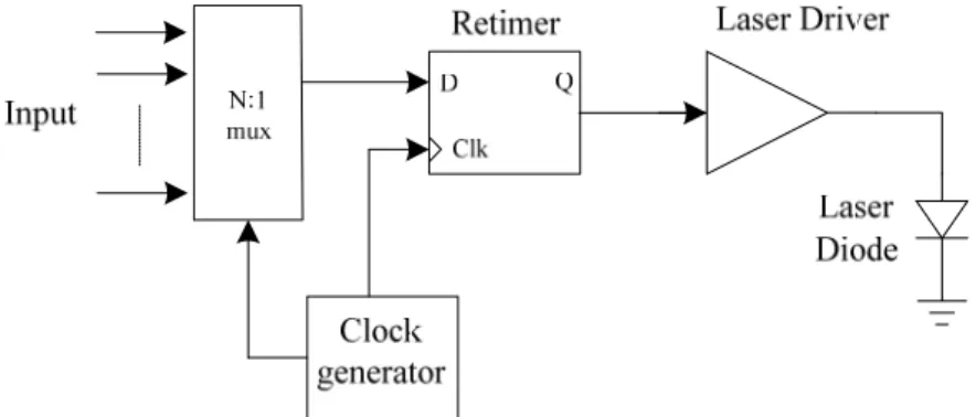
1-2 Transmitter
Fig. 1.2 shows a typical fiber optic transmitter. A multiplexer manages parallel input
data in the form of many low-speed channels and interleaves them into a serial one. The task
of parallel-to-serial needs a precise clock generator to align each data phase. As scaled
technologies impose lower supply voltage and rapidly growing bandwidth, the output of mux
may suffer from intersymbol interference (ISI) and jitter, so we need to retime the data to
become a pure stuff we want. Since the jitter of the transmitter is determined primarily by that
of clock generator, a low-noise design (e.g. frequency synthesizer) becomes essential. Finally,
a laser driver plays a simple current switch to turn on or of the logic value, also it’s
assignment is likely so easy, a good laser driver should bear large voltage swing and generate
high output current that laser diode required [2].
There are many advanced techniques that can enhance signal precision. For example, a
binary source may be encoded in an FEC [3] encoder to reduce bit error rate, low-pass filter
limits the channel code signal, and a scrambler randomize 0 and 1 distribution, etc.
Fig. 1.2 Fiber-optic transmitter
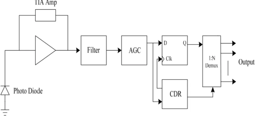
1-3 Receiver
Fig. 1.2 shows a typical fiber optic receiver. Inversely, the light travel through a long
way to far end and bump against photo diode first, the power of light is then transformed into
current mode, which is subsequently amplified and converted to voltage by the
transimpedance amplifier (TIA). Designer should modify all the trade-offs carefully about
TIA because it would affect the follow one. An automatic gain control amplifier (AGC) is to
amplify input signal to a predetermined amplitude, it’s similar to Limit amplifier (LA).
Because of many impairment induced by the channel, we also put a flip-flop block which’s
like the retimer mentioned before to clean up noise and line up data. We must notice that
there’s no clock generator to make a well-defined phase clock, however, one of the most
important block named the clock and data recovery (CDR) is introduced here. CDR can
extract many phase of clock from dirty data, and it should satisfy stringent specifications
defined by optical standards. We’ll go into details in Chapter 2.
Fig. 1.3 Fiber-optic receiver
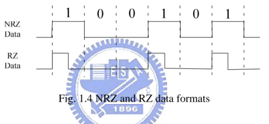
1-4 NRZ and RZ
Most optical communication systems employ binary amplitude modulation for ease of
detection. Several line codes can be used for representation of a data stream. We present two
more popular codes, return to zero (RZ) and non-return to zero (NRZ) that are illustrated in
Fig. 1.4. The former consists of two sections: the first bit assumes the bit value and the second
bit is always zero. The latter distinguishes it from RZ, in which it’s only one bit to carry one
value.
Fig. 1.4 NRZ and RZ data formats
Fig. 1.5 shows the spectrum density of two line codes, In contrast to NRZ and RZ data
format, RZ data stream exhibit a spectral line at its frequency, but the spectrum of NRZ data’s
bit rate is just right zero. The draw back of RZ is twice as much bandwidth as NRZ data does.
Although it’s harder to extract clock for NRZ coding, we usually choose it in high-speed OC
system for the trade-off in circuit design.
Fig. 1.5 PSD of NRZ and RZ data
1-5 Organization of the Thesis
This thesis comprises four chapters. To fully understand why CDR plays such an
indispensable role in OC system, it’s slightly interpreted as previously. But in order to start the
detail of this paper, chapter 2 takes our step ahead. It discusses full rate/half rate and quarter
rate’s trade-off, and describes why we use two loops to improve the acquisition time. In
chapter 3, we present how to realize the 1.25Gb/s quarter rate CDR. As we close the loop to
lock the phase, more trade-off need considering about. Because of many ready-made clock
phases, it allows the demultiplexer to divide the data into four streams. Although this is less
significantly than an actual serial 1.25Gb/s output, it is sufficient to demonstrate feasibility.
Comparison are spread on chapter 4, and some suggestions for future work on this topic are
also given.
Chapter 2
Clock and Data Recovery Architectures
2-1 Principle of Operation
This chapter discusses the principle of operation related to the CDR architectures. A
common approach to CDR is the use of phase-locked loop (PLL) [4], [5] because of its
suitability to monolithic integration. The function of each building block is presented on Fig.
2.1 [6]. As phase detector recognizes the difference phase between data and recovery clock,
the gain of it will transform to current by charge pump (CP). Recall from chapter 1 that jitter
induces from channel will impair correct data, so jitter tolerance is a target we should face.
We could limit the bandwidth to provide suppression of the phase noise by low pass filter
(LPF), the trade-off is that it will lower down totally operation frequency. Luckily, several
proposals scheme have been reported.
Fig. 2.1 Conventional simple one loop CDR
2-2 Phase Detector
The bang-bang CDR architectures have recently found in high speed applications [7] [8].
As illustrated in Fig. 2.2, we will find a very high gain and a zero gain in the vicinity of Δψ
=0 and elsewhere. Despite it exist a finite slop arises in actual case, the advantage of high can
indicate easily if the data is early or late. The characteristic of D Flip-flop (DFF) exhibits an
extremely nonlinear behavior, as a result, there’re many CDR architecture designed using
DFF phase detector.
Fig. 2.2 Bang-bang PD characteristic
Alexander reported a bang-bang CDR circuit for low-power and high-bit-rate operation
[9], which works at a full-rate clock frequency. As depicted in Fig. 2.3, three point S0、S1 and
S2 sample data to decide whether clock is early or late. The Alexander PD offers two critical
excellences over only one DFF PD: its output period is the same as the bit rate and retimes the
data automatically. Second, a consecutive identical digit (CID) pattern of zero will not disturb
the oscillator control.
D
Q
D
Q
D
Q
D
Q
LPF
Charge
Pump
VCO
Input
Fig. 2.3 CDR circuit using Alexander PD
But it maybe difficult to design oscillators when achieving higher operational speed in
OC system especially we still want to restrict jitter and power spec specification. For this
reason, CDR circuits may sense the input at full rate but employ a VCO running at half or
even quarter the input rate.
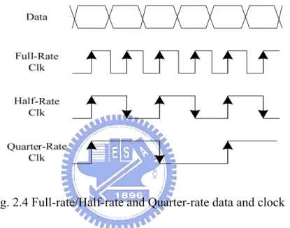
2-2-1 Operation Speed
Traditional CDR gets into problem to design a high-speed, low-jitter and low-power
receiver. Therefore, novel techniques must be devised to guarantee the reliability and
performance. Such new architectures with half-rate [7] and quarter-rate have already been
reported in the literature.
Fig. 2.4 Full-rate/Half-rate and Quarter-rate data and clock
Fig. 2.4 shows the contrast of three data rate. We need only single edge flip-flop to
sample data in full-rate, but as the oscillator frequency scale down, double edge flip-flop is
performed to trace the phase difference. While we scale down the oscillator frequency, we
also reduce the power dissipation in the way. The trade-off is that the duty cycle becomes
more and more important for locking the right phase. The comparison with Full-rate/Half-rate
and Quarter-rate CDR is listed in Table 2.1. Another advantage of half/quarter rate is that we
can parallel the output to make them suitable for fiber OC system.
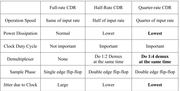
Full-rate CDR Half-Rate CDR Quarter-rate CDR
Operation Speed Same of input rate Half of input rate Quarter of input rate
Power Dissipation Normal Lower Lowest
Clock Duty Cycle Not important Important Important
Demultiplexer None at the same time Do 1:2 Demux Do 1:4 demux at the same time Sample Phase Single edge flip-flop Double edge flip-flop Double edge flip-flop
Jitter due to Clock Large Lower Lowest
Table 2.1 Comparison with Full-rate/Half-rate and Quarter-rate CDR
A quarter-rate CDR [10] based on Alexander PD is reported. The Phase detector uses
clocks with 45° phase steps in between, to capture the data with eight flip-flops. It is Similar
to Alexander PD that each XOR compares two outputs of DFF. Fig. 2.5(a) (b) shows the
timing chart and architecture of the structure. In the lock condition, the result of XOR would
be a trail of consecutive ones or zeros. Otherwise, we will get all ones or zeros. To compare
the quarter-rate architecture of this one with original full-rate Alexander PD, The numbers of
DFF are 2 times of later one and XOR gates are also increase. That is what we compromise.
The same result is accomplished in Fig. 2.5(c) to decrease area and ripple on the control line.
It also reduces the VCO jitter [11].
(a)
(b)
(c)
Fig. 2.5 (a) Architecture of the phase detector, (b) timing chart, and (c) modified
2-3 Frequency Detector
Recall that the loop bandwidth should be small enough to improve noise performance
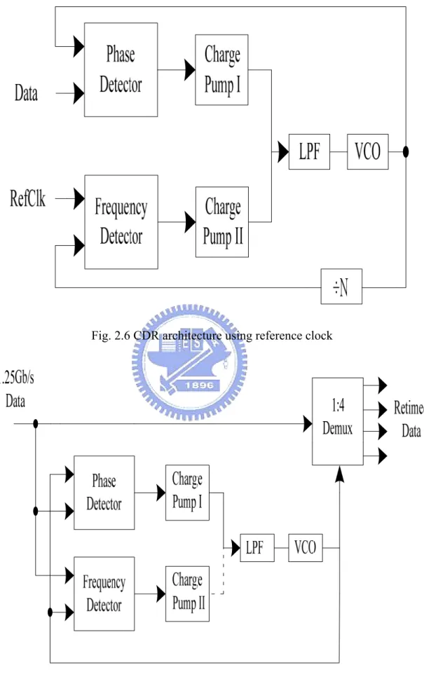
[12], it will cause small capture and pull-in ranges however. A CDR architecture using an
additional reference clock [13] might be as shown in Fig. 2.6. This two loops CDR firstly try
to lock the oscillator by reference clock. Until the frequency error is well, the phase detector
will tune it up to the correct point. We can improve a level of capturing time. Nevertheless,
this kind of two loops sometimes can’t perform a smoothly switch from one loop to another
loop. VCO frequency may jump outside of capture range out of hand.
Fig. 2.6 CDR architecture using reference clock
Fig. 2.7 Proposed CDR architecture using two loops
A method of alleviating jitter is to add another VCO rather than reference clock. It will
decompose the VCO control into “fine” and “coarse” loop to do more fine tuning. Of course,
only fine control may not provide enough tuning range to encompass variations about
temperature or process, so coarse loop adds to lock. It is similar with the design mentioned
before, but we need to deal with frequency mismatches or oscillator pulling.
Fig. 2.7 shows our proposed CDR architecture using two loops without reference clock
and dual VCO. Worthy of saying that it is already applied to quarter-rate case. There is a
dotted line we care about. As FD locking the central frequency after a while, the path is
automatically removed to diminish the effect of itself. Two of CPs are needed to match
different V/I, one of it provide large current by positive feedback to enhance the frequency
acquisition, and the other one provides four-step currents to control the frequency of VCO.
We will discuss the frequency detailed in the next chapter.
2-3-1 Design of Frequency Detector
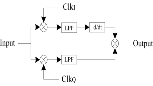
The directly thinking of the FD is called quadricorrelator [14], and it’s developed from
mathematic formula as in Fig. 2.8. We assume that input and clock are both periodic signals.
A multiplier (mixer) and a low pass filter can remove redundant noise and attenuate the high
frequency component. ClkQ lags behind ClkI of 90°. The output of the quadricorrelator will
have a dc component which is proportional to the frequency difference. However, as the VCO
frequency is almost toward to input frequency, (ω1-ω2) may sometimes fall to radical small
Fig. 2.8 Quadricorrelator
value and creating a large ripple. To avoid such situation, the digital version of the
quadricorrelator is adopted [15]. Fig. 2.9 (a) shows that we can use DFF to sample clock by
input to be viewed as an edge detector. It’s still need two clock paths to recognize if input
signal is faster or latter than clock frequency. As illustrate in Fig. 2.9 (b) and (c), if the clock is
faster than input and begin to sample the data from high level, output of Y will change to high
level after some cycles. Otherwise, suppose the clock is slower than input and begin to sample
the data from low level, output of Y will go to high after data edges drift enough. The
disadvantage of the digital version of quadricorrelator is that the capture range is not limitless
expand. Especially when we large our circuit and set several clock distributors. One way to
solve it is to modify PD or FD as a binary-to-ternary tristate operation [16].
(a)
(b)
(c)
Fig. 2.9 (a) Digital version of Quadricorrelator for (b) fast clock and (c) slow clock
Now, we develop a quarter-rate FD as shown in Fig. 2.10 (a). Eight DFF and four
DETFF are needed, in addition to four XOR and two OR gates. It’s based on the design of
quadricorrelator that clock is sampled by data. We can divide the timing chart (Fig.2.10 (b) (c))
into four states I, II, III, and IV by eight clock phases. To understand the operation of it, we
look detail of Fig. 2.10 (b) first. For a fast data example, we begin at IV state. If the frequency
error between data and clock is zero, then the output of XOR gates should be located on IV
state, too. But the second state appears on the III and the third one appears on the boundary of
III and II. In case of Fig. 2.10 (c) that is for the slow data example. The state transition rotates
from IV, I, II to III. According to the transit form, a digital quadricorrelator is also called a
rotational frequency detector.
(a)
(b)
(c)
Fig. 2.10 (a) Schematic of the FD, and its timing chart of (b) fast data and (c) slow data
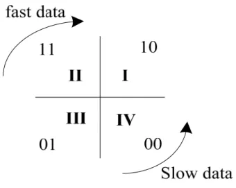
Fig. 2.11 State representation
Fig. 2.11 simplifies the representation of state rotation mentioned before. Another issue
needed to emphasize is that how the output of the state be stored. In general digital circuit
design, we always use flip-flop to hold the data. But in case of quarter-rate FD, each clock
phase has interval with 45° steps in between. Only single edge triggered will lose half of the
signal. Therefore, four double-edge-triggered-flip-flops (DETFF) are shown in Fig.2.10 (a).
From now on, we’ve already known how to detect and hold the difference between data and
clock. In order to feed the logic level to CP, the output of the DETFF is transformed by a
combinational logic gates comprised of five NAND and four INV gates to generate two
differentiate voltage level. Up and Down means that which direction the VCO frequency
toward to.
Fig. 2.12 Combinational logic gate
2-4 Voltage Controlled Oscillator
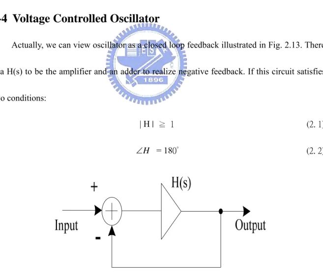
Actually, we can view oscillator as a closed loop feedback illustrated in Fig. 2.13. There
is a H(s) to be the amplifier and an adder to realize negative feedback. If this circuit satisfies
two conditions:
| H | ≧ 1 (2. 1)
H
∠ = 180° (2. 2)
Fig. 2.13 Feedback system
Then circuit may oscillate for a certain frequency. It’s so called Barkhausen’s oscillation
criteria, in addition to define it conscientiously: the steady oscillation requires a total phase
shift of 360° around the loop at a frequency where the small-signal gain is above 0 dB. To
meet the specification in high-speed, low-power integrated circuits, it’s common to utilize
voltage control oscillators (VCO). As shown in Fig. 2.14, obviously it’s a tunable application.
We can get different output frequency as we feed different input frequency. In ideal, we
always think a VCO as a linear modulation to simplify total design. However, in realistic
CDR systems, many issues like noise, bandwidth and frequency drift are affected by VCO
mostly. We will undertake some definitions to understand how to design a VCO what we need
[17].
Fig. 2.14 Model of a VCO
(1) Tuning linearity: the ideal characteristic of a VCO is shown in Fig. 2.15. It has an apparent
slope, Kvco, which is VCO gain. But actually oscillator exhibits nonlinear region that limit
the capture time with symmetry.
(2) Power dissipation: oscillators suffer from many trade-off like speed, power, and noise. In
recent years, power consumption becomes more and more essential to monolithic system
integration. Some proposals are published to achieve low power dissipation [18] [19].
(3) Output phase stability: Even with a constant voltage control input, the phase of the VCO
output maybe not fixed on the steady periodic. Noise and jitter are mostly caused by power
supply and signal path. We could use duty-cycle corrector to maintain a 50% duty cycle for
precise placement of phase [20].
Fig. 2.15 Characteristic of a VCO
Types of VCO LC-tank oscillator Ring oscillator
Operation speed Technology dependent 1-10’s of GHz Phase noise Good Poor Tuning range Narrow Wide Power consumption Low Medium
Process Monolithic Poor Excellent
Cost High Low
Other Multi-phase clocks
Table 2.2 Comparison between LC-tank oscillator and ring oscillator [21]
With reasonable requirements, the types of the VCO are separated into two parts named
LC-tank and ring oscillator. The comparison between two parts is listed in Table 2.2. LC-tank
oscillator has shown an excellent phase noise performance, good drive capability and high
speed. But it must cost a large number of inductors to achieve the tank quality even we could
stack inductors. Moreover, the limited tuning range of LC oscillator demands complicated
design such as mix with ring oscillator [8]. Thus, we take ring oscillator to be our choice. It
has inherent multi-phase clocks for the original purpose to FD and PD and suitable for
integration. Several attractive features above the discussion show that the ring VCO is a
promising candidate for this work.
2-4-1 Ring Oscillator
The ring oscillator using inverters is shown in Fig. 2.16. We can view each inverter as a
delay cell. Let’s recall what Barkhausen’s oscillation criteria saying, in a close loop, enough
gain and phase shift are needed to satisfy. Therefore, the frequency of this kind of oscillator is
given by: 1 2 d f Nτ = (2. 3)
where N is the number of inverters in the chain and τ is the delay time of each cell. d
Because every cell is just digital inverters, the phase shift of each cell equals 180°. N must be odd number to satisfy the criteria. If we notice the equation particularly again, it shows that
the decrease of N and τ can increase the frequency. But it doesn’t suggest any function d
about the power dissipation, we will consider that into gate level later. The drawback of ring
oscillator using inverters is the problem of insufficient gain (Fig. 2.17). The maximum phase
of each delay cell can provide is stationary 180° so it is hard to modulate the frequency except for changing the number of delay cell.
Fig. 2.16 Ring oscillator using inverters
H
∠
Fig. 2.17 Problem of insufficient gain
In standard CMOS processes, a simple differential common-source stage is used to
replace digital inverter (Fig. 2.18). Another pole which parasitic capacitor generates thereby
provides phase shift exceed 180° and the maximum is 270°. We can tune the capacitor to set
up total VCO frequency.
Fig. 2.18 Delay cell using differential common-source stage
2-5 Loop Filter
A loop filter lies between the VCO and CP to suppress high frequency components of
data. The passive second-order loop filter is adopted in this design which is consisted of a
resistor R and two capacitors C1, C2 as shown in Fig. 2.19. If we just focus on the serial R
and C1, the transfer function of the filter can be expressed as: ( ( ) K S z F s S ) ω + = (2. 4) Where z = 1 R1C1 ω , K = R1 (2. 5)
It is obviously to show that there are one pole on the original point to suppress high frequency
component when open loop, and one zero to increase the phase margin. Afterward, we
consider the other capacitor C2. It is used to add another pole to determine loop bandwidth.
( ( ) (1 ) z) p K S F s S S ω ω + = × + (2. 6) Where 1 1 1 2 R C K C C × = + , p 1 = R1(C1 C2) ω & (2. 7) Thus some important constant in the CDR can be calculated based on the pole and zero
like: p vco I K R 1 BW = 2 N 1 2 C C C π + (2. 8) And -1 -1 z p BW BW PM=tan -tan ω ω (2. 9) 26
Fig. 2.19 Second-order loop filter
Fig. 2.20 Loop response of third-order CDR
Fig. 2.20 shows the frequency response of the third-order CDR, where ωt is unit-gain
frequency. The goal of loop filter is to provide enough phase margin which is better between
30°~70°. However, it is always vied against response time and attenuation of noise. In general
case, we usually let
/ /
p t t z 4
ω ω ω ω
= = (2. 10)to give the phase margin 60°.
≈
2-6 Loop Performance Analysis
With the basically describing of CDR in anterior chapters, we can now analyze its
transient behavior. As the CDR is locked in a period of time, the effect of the frequency
detector can be neglected. We can construct a basic model without FD to give some analysis
as shown in Fig. 2.21 where means the gain of the phase detector and means the
gain of the VCO. Since the CDR is locked, a close-loop system is established. A close-loop
transfer function is given by:
d K Kvco
( )
( )
o vco d i vco dK
K F s
s
K
K F s
θ
θ
=
+
(2. 11)where θi and θo denote the phases of the input and output waveforms, respectively. The
function of (2. 11) tells us θo cannot fully track θi as possible because it is taken a first
order low pass filter to simplicity. It’s another way to visualize the behavior of transient time
especially we want to take frequency into account.
d
K
F s
( )
θ
o
o
θ
K
vcoS
28Fig. 2.21 CDR basic model without FD
2-6-1 Damping Factor
For the close-loop system, stability is a critical issue to compare whether the CDR will
go into lock. Sometimes we use the parameter of damping factor to predict the behavior in
advance. Let’s consider the step response first illustrated in Fig. 2.19. The observation is that
if input changes very fast which is similar to a step, output may be overdamped, damped or
underdamped. To derive the condition in easy way, it is lucky that we can use some equation
to express: 1 2 p d v c o K K ω ζ = (2. 12)
Another way to describe it was:
1 2 n p
ζ ω
=ω
(2. 13) Whereω
n=
ω
pK K
vco d (2. 14)Illustrated in Fig. 2.22 for several ζ values, we can view that the response is more and
more underdamping as ζ getting smaller and it will cause ripple on the VCO control line.
Therefore, to choose ζ > 0.707 or even 1 is a better way. In equation (2. 13), it implies that
how settling time and noise are trade-off. Lower ωp may suppress the high frequency
components but slower the response time. Fig. 2.23 shows the frequency response of
second-order system and it was normalized already. It reveals again the characteristic of low
pass filter and overdamping effect.
0.5
ζ
=
0.2
ζ
=
0.707
ζ
=
Fig. 2.22 The transient response of CDR to a frequency step
(
ω ω
/
n
)
1
ζ
=
3
ζ
=
0.707
ζ
=
30Fig. 2.23 Frequency response of the CDR
Chapter 3
A 1.25Gb/s Quarter Rate Clock and Data Recovery
Design
3-1 Introduction
This chapter continues from the preceding paragraph and introduces detail of 1.25Gb/s
quarter rate clock and data recovery design. The circuit is fabricated in 0.35μm CMOS
2P4M process and operated in central frequency of 312.5MHz using 3.3V power supply. The
process variations and temperature effects are tested in several corners of simulation.
Moreover, we will consider the pattern of pseudo random binary sequences to manifest the
reality of CDR. This CDR circuit employs a quarter-rate architecture to relax the speed
requirement and the proposed VCO, PD and FD topologies achieves a lower power
dissipation than of previous work.
3-2 Circuit Description
3-2-1 Phase Detector
The phase detector uses a four step bang-bang schematic which is like Fig. 2.5 (c) as
shown in Fig. 3.1. The obvious change is that we add three DFF but still four XOR. Totally
eight DFF will track the input data by eight clock signals and it will increase trigger
opportunity. Every clock phase is shifted by π/4 the same as Fig. 2.5 (a) and the sampling is
performed in sequence. However, output data of the DFF are not compared every two
consecutive using XOR gates. For instance, first of the XOR compares the data triggered by
clk0 and clk1, and the second one compares the data triggered by clk2 and clk3. The
relaxation of the comparison will reduce the ripple on the VCO control line which causes the
VCO output jitter. It is likely a tri-state comparator as shown in Fig. 3.2. Only continuous two
Pull-up triggers can lead output to VDD or it will bring to a middle point. It is important to
reassert that the purpose of the PD is lock the phase as soon as possible but is required to
conform to the jitter tolerance. Finally, the pulses of the four XOR gates represented are used
to charge or discharge the current by charge pump. Above all, we can calculate the PD gain
now. Because of four step generation of PD output, the current flows through loop filter will
be 1 2I KL
± i where K is the dc gain of loop filter. It is a tri-state method, too. We can’t get
VDD or truly GND until we meet continue two PDup or PDdo. Due to four step bang-bang
detector, we could try to the think tri-state as characteristic of linear to calculate the PD gain
easily [22]. When θe reaches the interval of π, it will generate totally IL to flow through
charge pump. Thus,
2 L d I K π = (3. 1)
The True-Single-Phase-Clock (TSPC) [23] is what we use for DFF illustrate in Fig.3.3,
where only one clock phase simplify the layout wire. The design is classified as a
Master-Slave register. As Clk is high, the flip-flop will sample D and store until Clk get low.
Fig. 3.1 Proposed architecture of the phase detector
Fig. 3.2 Timing chart of the proposed PD waveform
The great advantage is this kind of DFF is that it can operate at very high speed and
simple circuit structure. To notice that we put an inverter chain at the output for increasing the
capacity of pushing the circuit following. Fig. 3.4 shows a digital XOR Schematic [24] and it
consists of a transmission gate and two MOS. The operation of it is shown as following.
When A is low, B is transmitted into output Y directly by transmission gate. Otherwise, the
transmission gate would be closed as A is high. And the output Y will be determined by two
MOS and active as an inverter. So we could give the logic as a function:
Y=A♁B (3. 2)
Fig. 3.3 Schematic of TSPC DFF
Fig. 3.4 Schematic of XOR gate
3-2-2 Frequency Detector
In order to reduce the power dissipation and area, we try to decrease the use of DFF in
Fig. 2.9 (a) since it is one of our destinations to make use of quarter-rate. After modifying the
architecture, we also smooth the transfer of control authority. As mentioned before, FD is
needed to remove after the phase error is small enough. If the transfer is not smoothly well, it
may result in unpredictable ripple and narrow the capture range. It is right the opposition of
what FD does. In practice, the transfer of rotational frequency is used either periodic or
random input data pattern. Moreover, we can always get the result that acquisition rate is the
inverse of frequency error. It is to say that lock-in range and capture time are sometimes
trade-off. Thus, we choose the new architecture to slightly relax the take over to be sure of
wide lock-in range.
Fig. 3.5 Proposed architecture of the frequency detector
Fig. 3.6 Schematic of DETFF gate
Lastly, the FD needs the Double-Edge-Trigger-Flip-Flop (DETFF) to hold the signal that
is already sampled. Fig. 3.6 shows a modification of the DFF enabling sampling on double
edges. It consists of two parallel DFF which is active for opposite clock signal. Although it
increases the area of the circuit but only raise a little power consumption since there are
always half of the circuit active.
3-2-3 Voltage Controlled Oscillator
We have talked about VCO in chapter 2. And based on several comparisons, we’ve
taken ring-oscillator to be our choice. At the moment we can introduce our propose VCO
architecture. Fig. 3.7 shows the building block of VCO and it consists of four delay cells. For
our purpose of CDR, 45° phase shift of clock signal are needed and that means we have to
implement a ring oscillator with four stages at least. Extra circuit compare with the original
differential common-source stage are positive partial feedback [25] and symmetric load [26].
The positive partial feedback is contained by a cross-coupled pair. It exhibits a negative
resistance of -2/ but the total equivalent resistance will increase, thereby it increase the
gain of the cell, too. The use of the positive partial feedback generates appropriate gain to
conform to the Barkhausen’s oscillation criteria and only add simple circuit rather than
enlarge the size of the bias current source. That is other way to avoid additional power
consumption. Further, the symmetric load is formed by diode-connect PMOS devices to be
shunt with equal sized PMOS. That substitutes the resistor R in order to improve static and
m g
Fig. 3.7 Schematic of four stages VCO and its delay cell
Fig. 3.8 Proposed VCO with control region
dynamic supply noise. It allows to diminish the sensibility to variation of common mode and
to enhance the quality of noise rejection. Although the I/V curve of it is still nonlinear but the
capacity of noise immunity is greatly advanced. Besides, there is a Vcon node which can be
changed to tune the delay time along with oscillator frequency. The transfer function of the
proposed delay cell is:
0 1 ( ) [ ] 1 z p s H s A s ω ω − = + (3. 3) Where 0 1 m ma g R A g R = − , m p gd g C ω = , 1 ( ) ma z L gd g R C C R ω = − + (3. 4)
And A0 is the low frequency gain, ωpandωzare the pole and zero of the frequency, and
are respectively the trans-conductances of positive partial feedback. At last, R is the
resistance of symmetric load.
ma g
m g
Fig. 3.8 presents the delay cell with control region [19]. They can both control the delay
time and bias current, which provides a polarization to the cell. Without the mechanism, the
amplitude of the output will not be constant as soon as the frequency changed. A
diode-connect NMOS is parallel with the control input device. It is to be sure at least
minimum current flow though the circuit to start up the oscillator.
3-2-3-1
Duty-Cycle Corrector
Recall that to maintain a duty-cycle for precise placement of phase is more and more
important in high-speed application. Particularly, we have several clock signals and operate
(a)
(b)
Fig. 3.9 (a) Schematic of feed forward duty-cycle corrector and (b) its timing diagram
them at quarter-rate. Irregular rising or falling time may sometimes result in unsuccessful
sampling. Thus, we add an additional circuit called duty-cycle corrector [20] to stabilize the
VCO output. As shown in Fig. 3.9, it is a type of feed forward instead of feedback to
eliminate the extra feedback hardware. A leading and lagging signal are fed into the input
nodes, to notice that the original signals are a little close to sin wave and get irregular rising or
falling time. The duty-cycle corrector utilizes these two signals from differential VCO to
charge and discharge the signals again. For instance, as signal A goes low, the charge path will
go on but the discharge path will cut-off because that signal B goes high. It is quite the
contrary as signal goes high. Since the circuit consists of only a transmission gate and two
inverters, we can ignore the effect of additional power dissipation.
3-2-3-2 Linearization Circuit
Although the control region has balanced the VCO frequency and the amplitude of
output signal, we still got some problem of nonlinear effect. If the VCO control voltage is not
linearly proportional to the output frequency, the sensitivity of turning range will be harmful.
Therefore, we must limit the tuning range of voltage by linearization circuit [27] as shown in
Fig. 3.10. The mechanism of it is we only fetch certain division of input that is linear and
ignore other region. The advantage is that we linearize the capture time but the trade-off is we
need to increase the gain of the VCO for widen capture range.
(a)
(b)
Fig. 3.10 (a) Schematic of linearization circuit and (b) its Vin/Vo curve
(a)
Fig. 3.11 The transfer curve of VCO (a) without linearization circuit and (b) with it
3-2-4 Charge Pump
There are two charge pumps we need to transform phase and frequency error into
current. We have implied that one of them provides large current by positive feedback to
enhance frequency acquisition, and the other one provides four-step currents to control the
frequency of VCO. It’s common to use two switched current source that pump charge into
loop filter but the charge sharing and charge injection phenomenon will lead output a jump.
Thus, we introduce two modified design.
3-2-4-1
Charge Pump 1
Fig. 3.12 shows the schematic of charge pump 1 [28] which overcomes the charge
sharing and charge injection phenomenon. The most important is it can be used for four-step
currents to control VCO frequency. We can notice that real control inputs are not directly
effect output nodes that will suppress charge injection slightly. Moreover, the current source is
placed far from control signal in order to attenuate switch error. Even every control signals are
off, the output node can be charged to certain point by current source and current mirror.
However, there is still charge sharing effect that will generate a pulse at output in a short time.
For example, we assume the control signals are off in Fig. 3.13, and the Vds of both control
device will set to be zero by capacitance of drain-source. The output charge will be shared by
these parasitic capacitances. Therefore we add two MOS (Mn and Mp) to remove the
phenomenon [29].
Fig. 3.12 Schematic of charge pump 1
(a) (b)
Fig. 3.13 (a) Charge sharing phenomenon and (b) eliminated by additional devices
3-2-4-2
Charge Pump 2
The charge pump used for the following of FD is in order to increase the frequency
acquisition. By means of this issue, large current is what we want but it can’t also generate
much power consumption. We choose the design of Fig. 3.14(a) [30] to realize it. It consists
of a positive feedback mechanism to reuse current. As Up goes low, A will charge to VDD by
two paths to cut off output device. One of them is by taking away the discharge path, ant the
other path is charged by current mirror. It is a kind of positive feedback to reuse current. Even
so, as Up goes low, it will not get advantage from the architecture to save power consumption.
Luckily we have another modified one which can solve the problem [31]. As shown in Fig.
3.14(b), by adding a parallel PMOS device we can symmetrically realize current reuse. The
total charge pump 2 is shown in Fig. 3.15 and formed by two current reuse charge pumps. By
the way, the amount of switching speed is determined by the ratio of current mirror and
positive feedback gain. To suitably choose the ratio for the sake of speed and power is a
trade-off.
3-2-5 Demultiplexer
In high-speed OC systems, a demultiplexer (Demux) is a key component to measure and
demonstrate retimed data. It allows us to separate a serial data into a parallel stream that is
lower than original speed to somehow avoid the attenuation and increase the bandwidth in the
channel. Fig. 3.16 (a) is a block diagram of 1:4 Demux [32] [33]. It consists of three 1:2
(a) (b)
Fig. 3.14 (a) Original current reuse charge pump and (b) its modify
Fig. 3.15 Schematic of the charge pump 2
Demuxs and a frequency divider. And each 1:2 Demux employs five DFF to generate two
outputs. The operation of the 1:2 Demux is to execute two sample paths named three-stage
DFF (TS-DFF) and maser-slave DFF (MS-DFF). The sample point of MS-DFF is lag behind
TS-DFF for one bit and the different sample point automatically come into effect of
demultiplexing. The disadvantages of this architecture are the need of frequency divider and
numerous DFF. Additional frequency divider may induce clock skew that will impair the
alignment of next Demux and different clock sometimes degrades the setup time and hold
time margins limiting the whole speed. To alleviate the problem of above description, we try
to modify the original design. Recall that we have designed a multi-phase VCO. This is the
time to utilize it. Fig. 3.17(a) shows that we use different clock signal with phase shift of 90°
rather than the same clock signal to sample data. That will reduce the need of frequency
divider and one 1:2 Demux. Now, we can demultiplex the data in to four signal stream at the
same time and decrease the power dissipation as shown in Fig. 3.17(b).
1:2Demux
1:2Demux
Out0
Out2
Out1
Out3
(a) (b)Fig. 3.16 (a) a 1: 4 Demux tree architecture and its component: (b) 1:2 Demux
(a)
(b)
Fig. 3.17 (a) Modification of original 1:4 Demux and its (b) timing diagram
3-3 System Simulation Result
The clock and data recovery is implemented for the TSMC CMOS 0.35μm process and
simulated with HSPICE. Fig. 3.18 shows the frequency acquisition of different initial control
voltage with periodic input signal of 1.25Gb/s which is the same meaning of different initial
frequency. We can see that both the acquisitions are locked after about 2.2μs and stayed at
the voltage of 1.65V which is the middle of power supply. The waveform of periodic input
and retimed clock are shown in Fig. 3.19, and the retimed clock’s frequency is predicted
quarter-rate of input data. Fig. 3.20 is retimed data after 1:4 Demux. Because of periodic input
data, the retimed data will gradually be locked and set at the fixed value.
Fig. 3.18 Frequency acquisition of different initial control voltage with periodic input
Fig. 3.19 Periodic input data and retimed clock
Fig. 3.20 Retimed data after Demux
Fig. 3.21 shows the frequency acquisition with random data of -1 PRBS (Pseudo
Random Binary Sequence) using two comparison of different PD. Fig. 3.21(a) is our proposed
tri-state PD and (b) is the original binary-state. Although the acquisition is faster in (b) but it
produces much more ripple after locked. The capture time is nearly 3.2μs and is definitely
slower than using random input. Fig. 3.22(a) is the simulation of retimed clock and retimed
data after 1:4 Demux. It can not be obviously seen that the relation between input data and
retimed data. But we can try to figure it out by Fig. 3.22(b) which is the eye diagram to show
the comparative frequency. The frequency of retimed data is quarter-rate of input data, and it
is conform to our anticipation. Jitter of the CDR is also can be calculated by eye diagram and
the resulting peak-to-peak jitter is simulated to be 130ps.
7 2
(a)
(b)
Fig. 3.21 Frequency acquisition with random input using (a) tri-state and (b) binary-state PD
(a)
(b)
Fig. 3.22 (a) Retimed clock and retimed data using random input and (b) those eye diagrams
Chapter 4
Conclusions and Future Work
4-1 Conclusions
A 1.25Gb/s clock and data recovery was presented in the thesis. We introduced a
dual-loop to improve frequency acquisition time and slow down VCO frequency to reduce
power consumption in chapter 2. In chapter 3, we increase the VCO gain by positive feedback
to conform to the Barkhausen’s oscillation criteria rather than enlarge the size of the bias
current source. At the same time, we use a 1:4 Demux to parallelize the retimed data to match
up the OC systems. Above all, we conclude some result of simulation to compare with the
thesis of others in Table 4.1. We get the advantage of the quarter-rate, such as low power and
acquisition time.
4-2 Future Work
Although we have several advantages of performance, some trade-off comes up at the
same time. Jitter tolerant is a critical issue in high-speed systems. We increase the speed and
reduce the power dissipation but also generate more peak-to-peak jitter at the VCO output and
retimed data. To reform the disadvantage of what we don’t want to anticipate, maybe we can
decrease some architecture to relax the acquisition.
[31] Our proposal
Input Data Rate 1.25Gb/s 1.25Gb/s
VCO Center Frequency 625MHz 312.5MHz
Output Data Rate 1.25Gb/s 4×312.5Gb/s
Power Consumption ~250mW ~25.5mW
Jitter 38.2ps 130ps
Acquisition Time 3.5μs 3.2μs
Power Supply 3.3V 3.3V
Technology TSMC 0.35μm CMOS TSMC 0.35μm CMOS
Table 4.1 CDR performance summary
Reference
[1] D. G. Goff, Fiber Optic Reference Guide, Boston: Focal Press, 1999.
[2] H.-M. Rein and M. Moller, “Design Considerations for Very High Speed Si Bipolar ICs
Operating up to 50Gb/s, ”IEEE Journal of Solid-State Circuits, vol. 31, pp. 1076-1090,
August 1996.
[3] Azadet, K; Haratsch, E.F.; et al, “Equalization and FEC techniques for optical
transceivers,” IEEE Journal of Solid-State Circuits, Vol. 37, pp.317-327, March 2002.
[4] M. Rein and C. Dorschky; et al, “A fully-integrated 40-Gb/s clock and data recovery IC
with 1:4 DEMUX in SiGe technology,” IEEE J. Solid-State Circuits. Vol. 36, pp.
1937-1945, Dec. 2001.
[5] G. Georgiou, Y. Baeyens; et al, “Clock and data recovery IC for 40Gb/s fiber-optic
receiver,“ IEEE J. Solid-State Circuits, vol. 37, pp. 1120-1125, Sept. 2002.
[6] B. Razavi, “Design of High-Speed Circuits for optical communication System” Proc.
CICC, 2001.
[7] J. Savoj and B. Razavi, “A 10Gb/s CMOS clock and data recovery circuit with a
half-rate linear phase detector,” IEEE J. Solid-State Circuits, vol. 36, pp. 761-768, May
2001.
[8] J. Savoj and B. Razavi, “A 10Gb/s CMOS clock and data recovery circuit with a
half-rate binary phase/frequency detector,” IEEE J. Solid-State Circuits, vol. 38, pp.
13-21, Jan 2003.
[9] J. D. H. Alexander, “Clock recovery from random binary signal,” Electron Lett., Vol. 11,
pp. 541-542,1975.
[10] J. Lee and B. Razavi, “A 40Gb/s Clock and Data Recovery Circuit in 0.18m CMOS
Technology,” IEEE Journal of Solid-State Circuits, Vol. 38, pp.2181-2190, Dec. 2002.
[11] P. Sameni and S. Mirabbasi, ”A 1/8-Rate Clock and Data Recovery Architecture for
High-Speed Communication Systems,” IEEE 2004.
[12] J. E. Rogers and J. R. Long,” A 10 Gb/s CDR/DEMUX with LC delay line VCO in 0.18
μm CMOS ,” IEEE Solid-State Circuits, Vol. 37, pp.1781-1789, Dec. 2002
[13] J. C. Scheytt, G. Hanke, and U. Langmann, “A 0.155, 0.622, and 2.488Gb/s Automatic
Bit Rate Selecting Clock and Data Recovery IC for Bit Rate Transparent SDH Systems,”
ISSCC Dig. Of Tech. Papers, pp. 348-349, Feb. 1999.
[14] C. F. Schaeffer, “The Zero-Beat Method of Frequency Discrimination,” Proceedings IRE,
Aug. 1942.
[15] R. J. Yang, S. P. Chen, and S. I. Liu, ”A 3.125Gb/s clock and data recovery circuit for the
10-Gbase-LX4-Ethernet,” IEEE Solid-State Circuits, Vol. 39, pp.1356-1360, Aug. 2004.
[16] Hideyuki Nosaka and Kiyoshi Ishii; et al, ”A 10-Gb/s Data-Pattern Independent Clock
and Data Recovery Circuit With a Two-Mode Phase Comparator,” IEEE Journal of
Solid-State Circuits, Vol. 38, No. 2, Feb. 2003.
[17] B. Razavi, RF Microelectronics, Upper Saddle River, NJ: Prentice Hall, 1998.
[18] Wei-Husan Tu and Jyh-Yih Yeh; et al, “A 1.8V 2.5-5.2 GHz CMOS Dual-input
Two-stage Ring VCO,” IEEE, AP-ASIC2004, Aug. 2004.
[19] D. P. Bautista and M. L. Aranda, “A Low Power and High Speed CMOS
Voltage-Controlled Ring Oscillator,” IEEE, 2004.
[20] Joonsuk Lee and Beomsup Kim, “A Low-Noise Fast-Locked Loop with Adaptive
Bandwidth Control,” IEEE Journal of Solid-State Circuits, Vol. 35, No. 8, Aug. 2000.
[21] Rich Walker, Short Coarse, ISSCC, Feb. 2002.
[22] K. Vichienchom and W. Liu, ”Analysis of phase noise due to bang-bang phase detector
in PLL-based clock and data recovery circuits,” in Proc. ISCAS 2003, Vol. 1, pp.
617-620, May. 2003.
[23] J. Yuan and C. Svensson, ”High-Speed CMOS circuit technique,” IEEE Journal of
Solid-State Circuits, Vol. 24, No. 1. pp. 62-70, Feb. 2001.
[24] P. John, Uyemura, CMOS logic Circuit Design, by Kluwer Academic Publishers, 1999.
[25] E. Wang and R. Harjani, “Partial Positive Feedback for gain Enhancement of
Low-Power CMOS OTAs,” Analog Integrated Circuits and Signal Processing, 8,
pp21-35, 1995.
[26] J. Maneatis, “precise delay generation using coupled oscillators,” IEEE Journal of
Solid-State Circuits, Vol. 28, No. 12. pp. 1273-1282, Dec. 1993.
[27] Sun-Ping Chen, “Design and implementation of a 3.125-Gb/s clock and data recovery
circuit,” M.S. Thesis, National Taiwan University, Department of Electrical Engineering,
June 2002.
[28] J. Maneatis, “Low-jitter process-independent DLL and PLL base on self-biased
techniques,” IEEE J. Solid-State Circuits, Vol. 31, No. 11. pp. 1723-1732, Nov. 1996.
[29] P. Larsson and J. Y. Lee, “A 400 MW 50-380 MHz CMOS programmable clock recovery
circuit,” in Proc. IEEE ASIC Conf. Exhibit, 1995, pp. 271-274.
[30] E. J. Hernandez and A. D. Sanchez, “A novel CMOS charge-pump circuit with positive
feedback for PLL application,” Electronics, Circuit and Systems, ICECS 2001. The 8th
IEEE International Conference, Vol. 1, pp. 349-352, Sept. 2001.
[31] Ming-Heng Tsai, “Design and Realization of a 1.25Gb/s Clock and Data Recovery
Circuit,” M.S. Thesis, National Chiao Tung University, Department of Electrical
Engineering, June 2005.
[32] K. Ishii and H. Nosaka, “4-bit Multiplexer/Demultiplexer Chip Set for 40-Gbit/s Optical
Communication Systems,” IEEE Transactions of Microwave Theory and Technique, Vol.
51, No. 11, Nov. 2003.
[33] Pinping Sun, Yong Lian and Aruna B. Ajjikuttira, “A 10-Gb/s, 1.5-Volt Low-Power 1:4
Demultiplexer for Optical Fiber communication,” ICASIC 2003. IEEE, Vol. 2, pp.
1082-1085, Oct. 2003.