Abstract—A novel on-chip transient voltage suppressor (TVS) integrated with the silicon-based transceiver IC has been proposed and verified in a 0.8 μm bipolar CMOS DMOS (BCD) pro-cess for IEC 61000-4-2 system-level electrostatic discharge (ESD) protection. The structure of on-chip TVS is a high-voltage dual silicon-controlled rectifier (DSCR) with±16 V of high holding voltage (Vh) under the evaluation of the transmission line pulsing (TLP) system with the pulse width of 100 ns. With the high holding current (Ih) of on-chip TVS, this design can pass±200 mA latch-up testing. Therefore, the on-chip TVS can be safely applied to protect the RS232 transceiver with the signal level of±15 V. The RS232 transceiver IC with on-chip TVS has been evaluated to pass the IEC61000-4-2 contact ±12 kV stress without any hardware damages and latch-up issue. Moreover, the proposed RS232 transceiver IC has been verified to well protect the system over the IEC 61000-4-2 contact±20 kV stress (class B) in the notebook applications.
Index Terms—Electrostatic discharge (ESD), RS232, silicon-controlled rectifier (SCR), transient voltage suppressor (TVS).
I. INTRODUCTION
T
HE system-level ESD protection to industrial electronics is absolutely necessary for reliability and safety [1]–[11]. The I/O interface of the industrial electronics must have the ESD protection solutions against IEC61000-4-2 contact (or air) discharge stress [12]. Moreover, direct pin injection of ESD stress at I/O ports had been used to emulate the cable discharged event (CDE) for the interface IC [13]–[15]. On-chip transient detection circuits with hardware/firmware codesign proposed in [1], [2] can release system locked or frozen states caused by ESD-induced transient disturbance. However, the hardware damage caused by CDE or direct pin injection at I/O ports cannot be protected by these designs. The maximum current of system-level ESD in IEC-61000-4-2 is 5 times higher than that of human-body-model (HBM) at the same zapping voltage. In general, the transient voltage suppressor (TVS) arrays areManuscript received June 24, 2013; revised September 28, 2013 and November 8, 2013; accepted November 29, 2013. Date of publication January 2, 2014; date of current version May 2, 2014. This work was implemented in the transceiver products of Amazing Microelectronic Corporation and has been issued the patent for the proposed on-chip TVS.
C.-H. Chuang is with the Department of Electronics Engineering and In-stitute of Electronics, National Chiao Tung University, Hsinchu 300, Taiwan, and also with the Department of R&D, Amazing Microelectronic Corporation, Hsinchiu 300, Taiwan.
M.-D. Ker is with the Department of Electronics Engineering and Institute of Electronics, National Chiao Tung University, Hsinchu 300, Taiwan (e-mail: [email protected]).
Color versions of one or more of the figures in this paper are available online at http://ieeexplore.ieee.org.
Digital Object Identifier 10.1109/TIE.2013.2297292
Fig. 1. Logic threshold voltage of RS232 signal for the driver side and receiver side.
Fig. 2. Traditional protection scheme for RS232 transceiver IC with off-chip TVS devices.
the best choice if the interface IC cannot provide the sufficient protection capability [16].
RS232 interface is widely used in industrial machines and scientific instruments for data communication. The logic threshold voltage of RS232 driver and receiver are shown in Fig. 1 [17]. The logic 1 voltage level is between −5 V and −15 V, and logic 0 voltage level is between 5 V and 15 V for RS232 signal. To protect the RS232 transceiver IC in general application, four off-chip TVS devices are necessary for two transmitter outputs and two receiver inputs, as shown in Fig. 2. The bidirectional TVS array should be taken into consideration
0278-0046 © 2014 IEEE. Personal use is permitted, but republication/redistribution requires IEEE permission. See http://www.ieee.org/publications_standards/publications/rights/index.html for more information.
5616 IEEE TRANSACTIONS ON INDUSTRIAL ELECTRONICS, VOL. 61, NO. 10, OCTOBER 2014
Fig. 3. Current discharge path of the traditional off-chip TVS design under ESD gun contact stress.
for bidirectional signal levels of the RS232 standard. The protection scheme of the off-chip TVS devices for RS232 ap-plication under the IEC 61000-4-2 direct pin injection has been shown in Fig. 3. The system-level ESD robustness depends on PCB trace layout and the clamping voltage of the off-chip TVS devices. The off-chip TVS devices should be placed close to the DB9 connector for increasing the inductance of PCB wire to release ESD current efficiently through the off-chip TVS devices. To get best system-level ESD performance, the right TVS devices have to be chosen and PCB layout guidelines should be followed. This may waste more PCB area and spend more R&D developing time.
In this paper, the RS232 transceiver IC with embedded on-chip TVS is proposed. The advantage of on-on-chip TVS pro-tection scheme is that system designers do not have to take care of the TVS device specification and the PCB layout for ESD protection [18], [19]. The direct pin injection system-level ESD robustness is depended on the RS232 transceiver IC itself. Moreover, the PCB space will be more compact by using RS232 transceiver IC with embedded on-chip TVS. The proposed structure of the on-chip TVS is a high-voltage dual silicon-controlled rectifier (DSCR) with high holding voltage (Vh) for latch-up free with RS232 signal. The proposed on-chip TVS with appropriate current limiter resistor and dimension of output driver design in RS232 transceiver IC has been evaluated to pass IEC 61000-4-2 contact±12 kV discharge by direct pin injection with small area of 236 μm× 236 μm. Moreover, the RS232 transceiver IC with on-chip TVS has been designed in the notebook, which has been verified to pass ±20 kV IEC 61000-4-2 (class B) contact discharge without any hardware damage and transient-induced latch-up issue.
II. NEWPROPOSEDON-CHIPTVS DEVICE
A. Design Considerations of On-Chip TVS Device for RS232 Application
The silicon-controlled rectifier (SCR) device has been pro-posed as on-chip ESD protection device with high ESD robust-ness in small layout area [20]–[25]. However, these previous designs were not suitable for RS232 application. The maximum rating voltage of the RS232 input stage of receiver is±25 V, so that the breakdown voltage of DSCR device has to be designed larger than±25 V without false triggered under normal circuit operation. The maximum signal level of RS232 transmitter is
Fig. 4. Layout top view and device cross-sectional view of the proposed high-voltage dual SCR device.
±15 V, so the Vh of DSCR is designed larger than ±15 V to ensure the signal integrity under ESD stress. Moreover, the high holding voltage (> 15 V) of DSCR device can make sure the latch-up free for RS232 transceiver IC. Moreover, in order to sustain system-level ESD stress with huge current, the turned-on uniformity has to be cturned-onsidered by layout design.
B. Device Structure
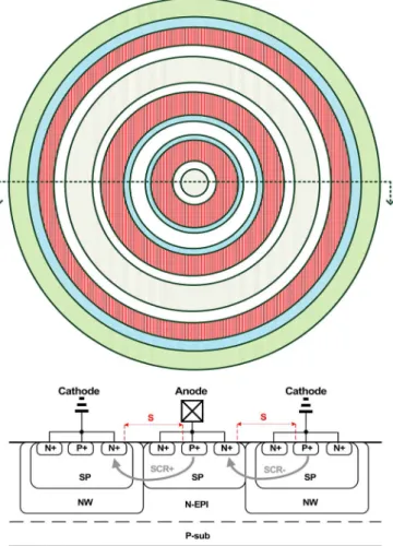
The layout top view and device cross-sectional view of the proposed on-chip TVS device are shown in Fig. 4. The device structure is shown in Fig. 5. The on-chip TVS device is a bidirectional high-voltage-triggered DSCR [26], which has been proven in the 0.8 μm bipolar CMOS DMOS (BCD) epitaxial process. When positive ESD stress is zapping at anode side, the ESD current will be discharged through the path of SCR+ which is indicated in Figs. 4 and 5. On the other hand, when negative ESD stress is zapping at anode side, the ESD current will be discharged through the path of SCR-. The p-n-p-n structures of the DSCR device for SCR+ and SCR-, as the arrow shown in Figs. 4 and 5, are both formed by symmetric layers of the P+ in SP, NW, SP and N+ in SP, respectively. Therefore, the DSCR device has symmetric I–V characteristics for positive or negative voltage stresses at anode side. The trigger voltage of the DSCR device can be adjusted by the different dosage of N-well (NW) with different breakdown voltage of SP/NW junction. The holding voltage of DSCR
Fig. 5. Device structure of the proposed high-voltage dual SCR device.
device can be adjusted by different spacing from anode to cathode with different βNPN× βPNPof DSCR device, which is indicated as S in Fig. 4. Therefore, the proposed DSCR device as on-chip TVS can be used on both transmitter output and receiver input in RS232 transceiver IC by suitable design of N-well dosage and spacing S. The layout style of the DSCR is circle type for current uniformity consideration to achieve highest ESD robustness. The inner circle is the anode side and the outer circle is the cathode side with the substrate guard ring. C. Evaluation on the Dual SCR
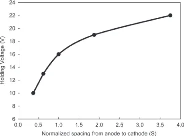
The secondary breakdown I–V curve of the DSCR device has been evaluated by a transmission-line-pulsing (TLP) system with the pulse width of 100 ns and the rise time of < 1 ns [27], [28], as shown in Fig. 6, where the normalized spacing (S) from anode to cathode is 1.0. The DSCR device under TLP measure-ment can get a TLP current up to 17 A without any obvious leakage current increased. According to the TLP I–V curve, the turned-on resistance (Ron) of the dual SCR device is 0.7 ohm in the holding region. The turned-on resistance of DSCR is larger than that of general off-chip TVS device because of the layout area limitation of the dual SCR device integrated in the I/O circuit of RS232 transceiver chip. The holding voltage (Vh) of the DSCR device is higher than ±16.0 V. Moreover, the holding current (Ih) of the DSCR device is 1.1 A, which is larger than maximum current driver of RS232 trans-mitter. Therefore, the RS232 signal will be still kept stable even if the DSCR was triggered. The dependence of normalized spacing S on the holding voltage is shown in Fig. 7. The holding voltage can be adjusted to higher than 16.0 V by modifying the spacing from anode to cathode. When the spacing S is increased, the holding voltage is also increased because the
Fig. 6. TLP measured I–V curve of the fabricated high-voltage DSCR device. The normalized spacing (S) from anode to cathode is 1.0.
Fig. 7. Dependence of holding voltage on the spacing (S) from anode to cathode in the DSCR device.
β-gain of the parasitic NPN (βNPN) and PNP (βPNP) in the DSCR device are reduced. However, the clamping voltage will also be increased by increasing spacing S. Therefore, the best selection of spacing S is as small as possible but still keeping latch-up free. The trigger voltage (Vt1) is 28.5 V, which is designed for 25.0 V of maximum rating voltage by adjusting the dosage of N-well for the input stage of RS232 receiver. The DSCR device can be turned on quickly before core circuit damaged to bypass ESD current under IEC61000-4-2 stress. From the evaluation result, the new proposed DSCR device is suitable for RS232 transceiver IC as on-chip TVS device.
III. DESIGNCONSIDERATIONS OFRS232 TRANSCEIVERIC WITHON-CHIPTVS A. Output Stage of Transmitter for RS232
For RS232 transceiver IC, the transmitter output and receiver input pins are connected to DB9 connector and have to pass IEC61000-4-2 ESD test. The overall design architecture of the RS232 transmitter output with on-chip TVS integration has
5618 IEEE TRANSACTIONS ON INDUSTRIAL ELECTRONICS, VOL. 61, NO. 10, OCTOBER 2014
Fig. 8. Current discharge path of the proposed on-chip TVS design embedded in transmitter output pin under ESD gun contact stress.
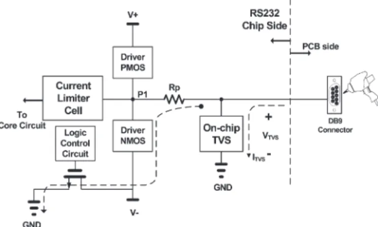
been shown in Fig. 8. The silicon implementation for on-chip TVS integrated in RS232 transceiver IC is much tougher than that of the off-chip TVS device. First, the process of the on-chip TVS itself must be fully compatible to that of the RS232 transceiver IC. Second, the ESD robustness of the output stage should be taken into consideration. Third, any RS232 core circuit connected to output stage (P1) should be blocked by a current limiter cell.
Unlike the off-chip TVS protection scheme shown in Fig. 3, there is no PCB wire inductor as current delay buffer but a designed resistor Rp between the on-chip TVS and the driver devices. The resistor Rp is added as the current limiter device to limit the ESD current into the driver and core circuit under ESD stress. For example, the secondary breakdown current of driver is 2.7 A (HBM 4 kV) and secondary breakdown voltage is 20.3 V; the VTVSof on-chip TVS has to be lower than 20.3 V under IEC 61000-4-2 contact 8 kV discharge if there is no resis-tor Rp. However, it is not a cost efficiency design for the on-chip TVS device in real products because of low clamping voltage which means large layout area consumption. If resistance of Rp is larger, the maximum VTVScan be larger and the layout area can be smaller of on-chip TVS. Moreover, for the design of the on-chip TVS protection, the device size of driver NMOS and PMOS should be estimated by the clamping voltage of the on-chip TVS device. If the VTVSof the on-chip TVS is higher, the size of the driver device should be larger for sustaining more ESD current. The layout area of the on-chip TVS has been limited so that the VTVS of the on-chip TVS device will be not smaller than that of the off-chip TVS device. Therefore, the ESD robustness of driver and the design of the resistor Rp are the key factors except for the on-chip TVS design to minimize total layout area and to get best ESD robustness.
Once the Vh and the Ron are obtained from the TLP system, for example, Vh is 16.0 V and Ron is 0.7 Ω which are indicated in Fig. 6, the clamping voltage of the DSCR device under IEC 61000-4-2 level 4 of 8 kV contact discharge (30 A within 1 ns) can be predicted as
VTVS= Vh + 30 A∗Ron = 37 V. (1) Assume the maximum resistance of Rp that can be designed is 8 ohm and the minimum clamping voltage of the driver NMOS or PMOS is 12.0 V, the maximum current through
Fig. 9. Current discharge path of the proposed on-chip TVS design embedded in receiver input pin under ESD gun contact stress.
the driver MOS is 3.125 A by 37 V of VTVS. Therefore, the ESD specification of the driver NMOS is above HBM 4.7 kV to make sure the internal device can still be alive under IEC 61000-4-2 contact±8 kV discharge. Compare to the original off-chip TVS design with HBM level of 4.0 kV, the total width of driver NMOS and PMOS should be increased a little with this proposed on-chip TVS design for RS232 transceiver IC to meet IEC 61000-4-2 contact±8 kV discharge.
To further protect the core circuit without ESD damage, the current limiter cell between P1 and core circuit is added to protect core circuit. The current limiter cell can be realized by a resistor of 1 ∼ 10 kohm in typical. The design of RS232 core circuit, which is connected to the node of P1, must be connected through the current limiter cell. The poly resistor is more preferred to realize the resistor Rp and current limiter cell than other resistors in the silicon substrate, because the poly resistor has no extra parasitic junction to be triggered on under ESD stress.
B. Input Stage of Receiver for RS232
The overall design architecture of the RS232 receiver input with on-chip TVS integration has been shown in Fig. 9. Unlike the output stage of transmitter, there is no output driver but input logic circuit after input resistor Rin. The gates of NMOS and PMOS devices in input logic circuit are connected to P2 which should be protected. Therefore, a reverse-biased diode D1 between P2 and GND which has lower breakdown voltage than gate oxide dielectric breakdown has to be designed. The Rin and RGare designed as 20 kohm and 5 kohm for consid-eration of RS232 receiver function, respectively. Assume the breakdown voltage of D1 is 10 V and VTVSis 37 V from (1), the maximum current through D1 is only 1.35 mA. Compare to the original off-chip TVS design, the device size of D1 is much smaller than that of traditional ESD protection device for HBM level of 4.0 kV. Therefore, the total layout area of input stage of receiver with embedded on-chip TVS can be smaller than that of traditional design.
C. Dual SCR as Embedded On-Chip TVS Design
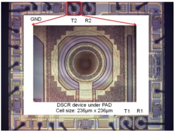
The whole chip of RS232 transceiver IC with DSCR de-vice as on-chip TVS in the I/O circuit is shown in Fig. 10. To efficiently reduce the layout area, the device under PAD
Fig. 10. Whole chip of RS232 transceiver IC with on-chip TVS in the IO circuit. The zoomed-in picture of dual SCR is shown in the center.
technique has been applied on the DSCR device with two metal layers [29]–[31]. The layout area for one DSCR device is 236 μm× 236 μm. Four DSCR devices are used in the RS232 transceiver IC to protect two transmitter outputs (T1 and T2) and two receiver inputs (R1 and R2).
The placement and routing of the on-chip TVS are important for discharging the ESD current efficiently. First, the metal width of GND should be drawn as wider as possible to reduce the current crowding effect. Second, the GND pad should be placed as close to the DSCR device as possible. Once the GND pad is closer, the parasitic inductance of wire line will be smaller to bypass the current with lower current delay and better ESD robustness. For example, in Fig. 10, all the four DSCR devices are with the same layout size and style. However, the distance of both T2 and R2 to GND is closer than that of both T1 and R1 to GND. From the experiment results, the T2 and R2 showed the better ESD robustness of 1 kV than that of T1 and R1 under ESD stress. Therefore, one more GND pad is suggested to be placed near to the T1 and R1 to efficiently discharge ESD current.
For single-chip ESD verification of RS232 transceiver IC, the VCC pin is floating. The ESD gun is with direct contact to the driver output or receiver input pin and ground line of ESD gun is connected to GND pin of chip to perform the direct pin injection of ESD stress. The DSCR device as on-chip TVS for the RS232 transceiver IC has been evaluated to pass the specification of the IEC 61000-4-2 contact±12 kV discharge without obvious leakage current increased under the single-chip ESD verification. After the stress of the IEC 61000-4-2 contact±16 kV discharge, some obvious damage spots located at the DSCR device in the circle-type layout but without internal damage, as shown in Fig. 11. The core circuit and driver MOS devices are without any damage. This means that the on-chip TVS device can really protect the internal circuit from ESD stress. The enlarged picture in Fig. 11 shows the “contact spike” uniformly located on the DSCR device, which means that the turn-on uniformity of on-chip TVS is good to discharge ESD current. Moreover, the RS232 transceiver IC with the proposed DSCR device as on-chip TVS device can pass±200 mA latch-up test.
Fig. 11. The SEM failure picture of the RS232 transceiver IC with on-chip TVS after IEC 61000-4-2 contact 16 kV ESD test.
Fig. 12. System-level ESD testing setup for RS232 transceiver IC with the proposed DSCR as on-chip TVS in the notebook application.
IV. SYSTEMVERIFICATION FORRS232 TRANSCEIVERIC For system verification of RS232 port under ESD stress, two notebooks with RS232 port but no TVS inside and one RS232 testing board with the proposed RS232 transceiver IC where the on-chip TVS design is embedded are setup and shown in Fig. 12. The equipment circuit of the system-level ESD testing setup is shown in Fig. 13, where the embedded on-chip TVS are at Rxin and Txout side of RS232 transceiver IC. The real-time data transmissions from notebook NB-A through the RS232 cable with the length of 2 m will be first received by receiver input Rxin of the RS232 transceiver IC. By loopback of receiver output Rxout to transmitter input Txin of the transceiver IC, the real-time data will be transmitted by transmitter output Txout of the RS232 transceiver IC to the notebook NB-B through another RS232 cable with the length of 2 m. The waveform of the signal at loopback Rxout (Txin) is observed by oscilloscope. The maximum Bd rate is 256 kb/s with 8 bits data by the NB software control. In normal transmission operation, the real-time data from NB-A to NB-B has been verified to have no error bit in the two thousand bits text file by comparison of the data to each other. The on-chip TVS will not be triggered on to cause function error during normal circuit operation. In the
5620 IEEE TRANSACTIONS ON INDUSTRIAL ELECTRONICS, VOL. 61, NO. 10, OCTOBER 2014
Fig. 13. Equipment circuit of the system-level ESD testing setup for RS232 transceiver IC with the proposed DSCR as on-chip TVS in the notebook application.
Fig. 14. Voltage waveform of signal at Rxout during IEC61000-4-2 ESD test of±8 kV in the notebook application.
ESD contact discharge test, the cable nears both Rxin and Txout sides of the RS232 transceiver IC will be zapped to evaluate the protection capability of the on-chip TVS in the data flow condition. The waveform of the signal at loopback Rxout (Txin) under±8 kV of IEC 61000-4-2 contact discharge is shown in Fig. 14. Under normal circuit operation, the voltage level of RS232 signal is±7 V. When the ESD stress occurred, the signal will be dropped to lower than RS232 minimum voltage level of ±5 V initially (at 1.2 ms). After 0.6 ms (at 1.8 ms), the voltage level will be auto-recovered to±7 V without any manual reset or hardware damage, and the real-time data flow will not be stopped. The Bit Error Rate (BER) is lower than 1% under ±8 kV of IEC 61000-4-2 contact discharge. During the IEC 61000-4-2±20 kV contact discharge, the real-time data flow will not be stopped but there is about 10% BER in the two thou-sand bits. The RS232 transceiver IC has been verified to have no hardware damage and latch-up issue after system-level ESD test. To sum up, the proposed RS232 transceiver IC with on-chip TVS protection has been verified to pass IEC 61000-4-2 ±20 kV contact discharge (class B, system can be
auto-TABLE I
ESDANDLATCH-UPRESULTS FORPROPOSEDRS232 TRANSCEIVER
IC WITHDSCR DEVICES ASON-CHIPTVS
recovered after ESD stress) in notebook system. It is reliable and safe to use the proposed DSCR device as the on-chip TVS device in the RS232 application.
The RS232 transceiver IC with the proposed DSCR device as integrated on-chip TVS has been fabricated and verified in the 0.8 μm BCD epitaxial process for system-level IEC 61000-4-2 ESD protection. The verification results for this RS232 transceiver IC with on-chip TVS integration has been summarized in Table I.
V. DISCUSSION
In this paper, the proposed DSCR device with suitable cur-rent limiter resistor and dimension of output driver is success-fully realized as on-chip TVS in RS232 transceiver IC. The on-chip TVS design for advanced transceiver such as USB, HDMI, and Thunderbolt will be studied in the future with the consideration of ultra low parasitic capacitance for high-speed I/O signals. How to implement the on-chip TVS with parasitic capacitance smaller than 0.5 pF in advanced nano-scale CMOS process to bypass such high system-level ESD energy in a reasonable layout dimension is the major challenge to be overcome in IC industry.
VI. CONCLUSION
Recently, direct pin injection of ESD stress at I/O ports has become a more stringent test to emulate ESD, CDE, or EOS events in the field applications. The RS232 interface must be equipped with strong ESD protection against system-level ESD stress of IEC 61000-4-2 contact (or air) discharge. The DSCR device as on-chip TVS integrated in the RS232 transceiver IC to sustain such huge ESD energy has been proposed in this work. With suitable current limiter resistor and the selected dimensions of driver MOS devices, the maximum design target on the clamping voltage of DSCR device can be calculated. The breakdown and holding voltages of the DSCR device have to be designed higher than±25 V without false triggered under normal circuit operation, as well as ±15 V without latch-up issue to ensure the signal integrity under ESD stress, respec-tively. The RS232 transceiver IC with on-chip TVS protection has been verified to pass IEC 61000-4-2 contact discharge (class B) of ±20 kV in notebook system without hardware damage and latch-up issue. The proposed DSCR integrated as on-chip TVS device has been successfully verified against system-level ESD stress in the RS232 applications.
[2] M.-D. Ker and C.-C. Yen, “New transient detection circuit for on-chip protection design against system-level electrical transient disturbance,”
IEEE Trans. Ind. Electron., vol. 57, no. 10, pp. 3533–3543, Oct. 2010.
[3] X. Wang, X. Guan, S. Fan, H. Tang, H. Zhao, L. Lin, Q. Fang, J. Liu, A. Wang, and L.-W. Yang, “ESD-protected power amplifier design in CMOS for highly reliable RF ICs,” IEEE Trans. Ind. Electron., vol. 58, no. 7, pp. 2736–2743, Jul. 2011.
[4] K. Thongpull, N. Jindapetch, and W. Teerapabkajorndet, “Wireless ESD event locator systems in hard disk drive manufacturing environ-ments,” IEEE Trans. Ind. Electron., vol. 60, no. 11, pp. 5252–5259, Nov. 2013.
[5] X. Perpiñà, X. Jordà, M. Vellvehi, J. Rebollo, and M. Mermet-Guyennet, “Long-term reliability of railway power inverters cooled by heat-pipe-based systems,” IEEE Trans. Ind. Electron., vol. 58, no. 7, pp. 2662–2672, Jul. 2011.
[6] S.-J. Cheng, Y.-K. Lo, H.-J. Chiu, and S.-W. Kuo, “High-efficiency digital-controlled interleaved power converter for high-power PEM fuel-cell applications,” IEEE Trans. Ind. Electron., vol. 60, no. 2, pp. 773–780, Feb. 2013.
[7] A. Ristow, M. Begovic, A. Pregelj, and A. Rohatgi, “Development of a methodology for improving photovoltaic inverter reliability,” IEEE Trans.
Ind. Electron., vol. 55, no. 7, pp. 2581–2592, Jul. 2008.
[8] C. Rodriguez and G. Amaratunga, “Long-lifetime power inverter for photovoltaic ac modules,” IEEE Trans. Ind. Electron., vol. 55, no. 7, pp. 2593–2601, Jul. 2008.
[9] T. Brodbeck, W. Stadler, C. Baumann, K. Esmark, and K. Domanski, “Triggering of transient latch-up by system-level ESD,” IEEE Trans.
Device Mater. Rel., vol. 11, no. 4, pp. 509–515, Dec. 2011.
[10] M. Scholz, S.-H. Chen, G. Vandersteen, D. Linten, G. Hellings, M. Sawada, and G. Groeseneken, “Comparison of system-level ESD design methodologies—Towards the efficient and ESD robust design of systems,” IEEE Trans. Device Mater. Rel., vol. 13, no. 1, pp. 213–222, Mar. 2013.
[11] M. Diatta, D. Trémouilles, E. Bouyssou, R. Perdreau, C. Anceau, and M. Bafleur, “Understanding the failure mechanisms of protection diodes during system level ESD: Toward repetitive stresses robustness,” IEEE
Trans. Electron Devices, vol. 59, no. 1, pp. 108–113, Jan. 2012.
[12] EMC—Part 4-2: Testing and Measurement Techniques—Electrostatic
Discharge Immunity Test, Int. Std. IEC 61000-4-2, 2008.
[13] W. Stadler, T. Brodbeck, R. Gärtner, and H. Gossner, “Cable dis-charges into communication interfaces,” in Proc. EOS/ESD Symp., 2006, pp. 144–151.
[14] M.-D. Ker and T.-H. Lai, “Investigation on robustness of CMOS devices against Cable Discharge Event (CDE) under different layout parameters in deep-submicron CMOS technology,” IEEE Trans. Electromagn. Compat., vol. 50, no. 4, pp. 810–821, Nov. 2008.
[15] W. Stadler, T. Brodbeck, J. Niemesheim, R. Gärtner, and K. Muhonen, “Characterization and simulation of real-world cable discharge events,” in Proc. EOS/ESD Symp., 2009, pp. 1–8.
[16] R. Chundru, Z. Li, D. Pommerenke, K. Kam, C.-W. Lam, F. Centola, and R. Steinfeld, “An evaluation of TVS devices for ESD protection,” in Proc.
IEEE Int. Electromagn. Compat. Symp., 2011, pp. 62–67.
[17] Interface Between Data Terminal Equipment and Data
Circuit-Terminating Equipment Employing Serial Binary Data Interchange, Int.
Std. TIA-232-F, 1997.
[18] R. Jiang, T.-K. Tseng, C.-H. Chen, and C.-H. Chuang, “Design of on-chip transient voltage suppressor in a silicon-based transceiver IC to meet IEC system-level ESD specification,” in Proc. IEEE ICIDCT, 2011, pp. 1–4.
Electron Device Lett., vol. 33, no. 5, pp. 640–642, May 2012.
[23] S. Dong, J. Wu, M. Miao, J. Zeng, Y. Han, and J.-J. Liou, “High-holding-voltage silicon-controlled rectifier for ESD applications,” IEEE Electron
Device Lett., vol. 33, no. 10, pp. 1345–1347, Oct. 2012.
[24] F. Ma, B. Zhang, Y. Han, J. Zheng, B. Song, S. Dong, and H. Liang, “High holding voltage SCR-LDMOS stacking structure with ring-resistance-triggered technique,” IEEE Electron Device Lett., vol. 34, no. 9, pp. 1178– 1180, Sep. 2013.
[25] W.-Y. Chen, E. Rosenbaum, and M.-D. Ker, “Diode-triggered silicon-controlled rectifier with reduced voltage overshoot for CDM ESD pro-tection,” IEEE Trans. Device Mater. Rel., vol. 12, no. 1, pp. 10–14, Mar. 2012.
[26] T.-K. Tseng, C.-H. Chuang, R. H.-C. Jiang, and M.-D. Ker, “Asymmetric bidirectional silicon-controlled rectifier,” U.S. Patent 8 049 247, Nov. 1, 2011.
[27] T. Maloney and N. Khurana, “Transmission line pulsing techniques for circuit modeling of ESD phenomena,” in Proc. EOS/ESD Symp., 1985, pp. 49–54.
[28] A. Jahanzeb, L. Lou, C. Duvvury, C. Torres, and S. Morrison, “TLP characterization for testing system level ESD performance,” in Proc.
EOS/ESD Symp., 2010, pp. 1–8.
[29] M.-D. Ker and J.-J. Peng, “Investigation on device characteristics of MOSFET transistor placed under bond pad for high-pin-count SOC appli-cations,” IEEE Trans. Compon. Packag. Technol., vol. 27, no. 3, pp. 452– 460, Sep. 2004.
[30] W. R. Anderson, W. M. Gonzalez, S. S. Knecht, and W. Flowler, “ESD protection under wire bonding pads,” in Proc. EOS/ESD Symp., 1999, pp. 88–94.
[31] G. Heinen, R. J. Stierman, D. Edwards, and L. Nye, “Wire bonds over active circuits,” in Proc. Electron. Compon. Technol. Conf., 1994, pp. 922–928.
Che-Hao Chuang received the B.S. and M.S.
de-grees from National Chiao Tung University (NCTU), Hsinchu, Taiwan, in 1999 and 2001, respectively. Currently, he is working toward the Ph.D. degree in the Institute of Electronics, NCTU.
Since 2006, he has been with Amazing Microelec-tronic Corporation, Hsinchiu, Taiwan, as the Man-ager for ESD protection design projects. His current research interests include TVS array development for system-level ESD protection, surge protection, and on-chip ESD protection design.
Ming-Dou Ker (F’08) received the Ph.D. degree
from the Institute of Electronics, National Chiao Tung University (NCTU), Hsinchu, Taiwan, in 1993. Currently, he is a Distinguished Professor with the Department of Electronics Engineering, NCTU, and also the Dean of the College of Photonics, NCTU.
Prof. Ker currently serves as the Editor of the IEEE TRANSACTIONS ONDEVICE ANDMATERI