A
Low-Voltage Fully-Integrated
4.5-6-GHz CMOS
Variable Gain Low Noise Amplifier
Ming-Da Tsai', Ren-Chieh Liu', Chin-Shen Lin' and Huei Wang"
'Graduate Institute of Communication and * Dept. of Electrical Engineering,National Taiwan University, Taipei, Taiwan, R.O.C.
Phone: +886-2-2363525 1 ext.3 17 Fax:+886-2-23638247 e-mail:[email protected]
Absrract
-
A 4.54 GHz CMOS low-voltage wideband variable gain low noise amplifier (VGLNA) with wide gain-control range has been demonstrated in this paper. The VGLNA, operating at a supply voltage as low as 1 V,achieves a small signal gain of 20 dB and 3-dB bandwidth of 1.5 GHz with good return losses. The noise figure is 3.5 dB at 5.5 GHz. A figure-of-merit for gain eficiency (Gain/PDc) of 1.23 dB/mW is achieved, which is believed to be the hest among reported results for a CMOS
VGLNA operating at multi-GHz frequency.
I. INTRODUCTION
The CMOS RF chips are getting more and more attractive owing to the advantages of low cost and integration ability with baseband circuits. LNAs using CMOS process have demonstrated good gain and noise per- formance in the 5-6 GHz ISM band [I-31. Variable gain low noise amplifiers (VGLNAs) were realized in order to maximize the overall system dynamic range [4].
A 1.4-dB NF variable-gain low noise amplifier using InGaP emitter HBT has been presented in [4], but
GaAs-based chip is difficult to integrate with CMOS
baseband circuits. A variable gain cascode amplifier using SiGe HBT technology has been demonstrated in [SI, however, the cascode topology is not suitable for variable-gain low noise and low voltage application [7]. A CMOS 900-MHz fully differential [6] and a CMOS 8-9-GHz low voltage [7] variable-gain low noise amplifier have also been proposed, but off-chip elements are required. In this paper. we used 0.18- m
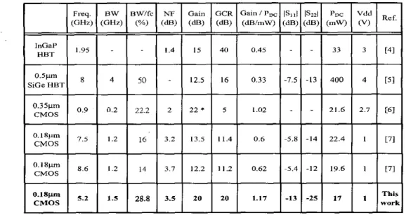
CMOS process to design a low-voltage Variable-gain low noise amplifier without any off-chip elements. Wide bandwidth is also achieved by splitting inter-stage matching frequency. Table 1 summarizes the recently reported performance of variable gain low noise amplifiers compared with this work. It is observed that
our chip demonstrated the widest bandwidth, gain-control range (CCR) and the best gain efficiency for a CjMOS VGLNA operating at multi-GHz frequency. The VGLNA chip achieves 20-dB gain, bandwidth of
1.5 GHz, noise figure of 3.5 dB, input return loss of 13
dB, and output retnm loss of 23 dB, operating at a low
Table 1. Recently reported pelformance of variable gain low noise amplifiers. B W 3-dB bandwidth. f,: center frequency. GaidPDc: the ratio of gain to dc-power-consumption [9]. The notation * means voltage gain.
I'dd
IN
4
Vdd
6
*
-
Fig. 1. Circuit schematic diagram of the folded cascode variable gain low noise amplifier. supply voltage of 1 V and 17 mW power consumption,
witha chip size of 1.2 x 1 mm2 using a 0.18-pm CMOS standard process.
11. CIRCUIT DESIGN AND FABRICATION In contrast to the conventional cascode FET, the VGLNA design employes a folded cascode structure in order to operate at a low supply voltage [7]. In this paper, VGLNA includes three portions: the first is the low-noise stage, the second is the gain control stage and the last is the gain stage. The schematic of this VGLNA is shown in Fig. 1.
Input matching, which is necessaty to minimize signal reflection and noise, is an important design issue. There is usually a trade-off between noise and input impedance matching in LNA design. The input matching is achieved by selecting
Lg,
L, and the gate-to-source capacitance(CgSl)
of the input NMOScommon-source transistor to fulfill the following
equations [SI:
where OW is the carrier frequency, g,, is transconductance of the input common-source transistor and R,,,, is the impedance of the signal source.
Between the two folded cascode FETs is an LC-tank
OUT
l-0
network, acting as a high impedance element at resonant frequency to force signal passing through the followed PMOS for overall small signal gain
(IS&
In our circuit, we design the resonant frequency slightly higher than the target frequency, 5-6 GHz. The second inter-stage impedance matching network is designed at about 4.2 GHz, slightly lower than in-band frequency, to compensate the narrow-band property of LC tank to achieve wideband performance. The LC tank network between low-noise stage and gain-control stage, shown in Fig. 1 is a high impedance network, and also supports bias current path to both stages. The main advantage of this LC-tank folded cascode design is that it does not require any off-chip element, such as RF-choke inductors. First LC-tank network and second inter-stage matching are designed to fit higher frequency and lower frequency, respectively. Simulation result of small signal gain is shown in Fig. 3.It is observed that operation frequency is from 4.2 - 6.5 GHz by splitting matching frequency.
The
gain-controlis
achievedby
modifyingthe
gate voltage of the PMOS common-gate transistor (Vgc) without affecting the bias condition and impedance matching, which are determined by the input NMOS common-source transistor. Hence, the optimum input noise is almost not affected when controlling the overall gain of this circuit. This CMOS VGLNA was fabricated using a 0 . 1 8 - ~ m standard CMOS process. A die micrograph is shown in Fig. 2. The chip size is 1.2 x 1 mm2.111. MEASUREMENT RESULTS
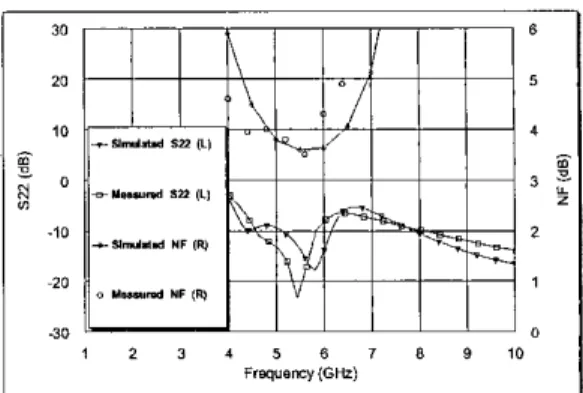
The circuit was measured via on-wafer probing. Figs. 3 and 4 show the measnred and simulated results of the
gain, retun loss and noise figure. With a power consumption of around 17mW from a 1 V supply, the
small signal gain is 20 dB with a 3-dB bandwidth of 1.5
GHz. The minimum input and output reflection coefficients are -13 dB and -23 dB respectively. The measured noise figure is only 3.5 dB at 5.6 GHz and below 5 dB in the frequency of interest. The measurcd results of S-parameters and noise figure agree with the simulation well. Variable gain performance with 2.5-dB gain steps from is shown in Fig. 5 . The GCR is about 20 dB while bandwidth is maintained over all
variable-gain condition. The variable gain control performance of the amplifier was achieved by current limiting of the common-gate PMOS in the folded cascode topology. The input PldB is -15 dBm. The measurement results show that this CMOS VGLNA design can operate properly at a high frequency with a low supply voltage down to 1 V.
IV. CONCLUSION
An ISM-band variable-gain low noise amplifier has been designed, fabricated, and tested. The VGLNA uses folded-cascode configuration and was fabricated by TSMC standard 0.18-pm CMOS technology. Our circuit demonsh.ated the widest bandwidth, gain-control range (GCR) and the best gain efficiency for a CMOS VGLNA operating at multi-GHz frequency. The VGLNA chip achieves a 20-dB gain, a bandwidth of
1.5 GHz, a noise figure of 3.6 dB, an input retum loss of 13 dB, and an output retum loss of 23 dB, operating at a low supply voltage of 1 V and 17 mW power consumption, with a chip size of 1.2 x 1 mm2 in a 0.lS-ym CMOS standard process.
Y ACKNOWLEGEMENT
This work is supported in part by the National Science Council (NSC ‘91-2213- E-002-042 and
NSC
91-2219-E-002-019) and the Research Excellence Program fund by the Ministry of Education, ROC (ME 89E-FA-06-2-4). The chip is fabricated by TSMC through the Chip Implementation Center (CIC), Taiwan, ROC. The authors would like to thank Kim-You Lin and Chi-Hsueh Wang, Taiwan, ROC, for the chip testing.
REFERENCE
[ I ] H. Samavati, H. R. Rategh. and T. Lee, “A 5-GHz CMOS wireless LAN receiver front end, “ IEEE J. Solid-State
Circuits, vol. 35, pp. 165.772. May 2000
[2] R. C. Liu, C. R. Lee, H. Wang, and C. K. Wang. “A
5.8-GHz two-stage high-linearity low-voltage low noise amplifier in a 0.35-pm CMOS technology.” IEEE RFlC S y n p Dig., pp. 221.224, 2002
[3] 1.1. W. Chiu. and S-S. Lu, “A 2.17 dB NF, 5 GHz baud monolithic CMOS LNA with 10 mW DC power consumption,” IEEE VLSI Circuits Symp. Dig,, pp. 226-229,2002
[4] Y Aoki, M. Fujii, S. Ohkubo, S. Yoshida, T. Niwa, Y. Miyoshi, H. Dodo, and H. Hi&. “A 1.4-dB-NF variable-gain LNA with continuous control for
2-GHz-band mobile phones using InGaP emitter HBTs,”
IEEERFICSymp. Dig., pp. 231-234,2001
[5] Q. Chaudhry, R. Alidio, G Sakamoto, and T. Cisco, “A
SiGe MMIC variable gain cascode amplifier,” IEEE
MWCL, pp. 424-425, Nov 2002
[ 6 ] E. Sacchi; I. Bietti, F. Svelto, and R. Castello, “A 2 dB NF,
fully differential, variable g a i ~ 900 MHr CMOS LNA,” IEEE VLSI Cirruits Symp. Dig., pp. 94-97,2000 [7] T. K. K. Tsang, and M. N. El-Gamal, “Gain controllable
very low voltage 8-9 GHz integated CMOS LNA’s,” IEEERFICSymp. Dig., pp. 205-208,2002
[XI
D. K. Shaffer, and T. Lee, “A IS-V, 1.5-GHz CMOS low noise amplifier, ‘’ IEEE J. Solid-Stare Circuits, vol. 32, p p . 745-759, Jun 1997191 K. W. Kobayashi, A. K. Oki, D.C. Streit, and L. T. Tmn,
“Ultra-low dc power GaAs HBT S- and C-band low noise
amplifiers for portable wireless applications,” IEEE Trans. on Mn. vol. 43, pp. 3055-3061, Dec 1995
16
Fig. 2. The die photo of the VGLNA with chip area of 1.2 x 1 mm'.
Fig. 3. The measured and simulated results of the power gain and input return loss.
1 2 3 1 5 B T 6 9 10
Frsquemy(GHi)
Fig. 4. The measured and simulated results of the noise figure and output retum loss.
Fig. 5 . The measured variable gain performance in 2.5-dB gain steps versus frequency, V,,= 0-1.8 V.