新式微波雙面校正與量測技術之發展與驗證
59
0
0
全文
(2)
(3) 新式微波雙面校正與量測技術之發展與驗證 指導教授:吳松茂 博士(助理教授) 國立高雄大學電機工程所. 學生:官聖洧 國立高雄大學電機工程所 摘要. 本論文提出新式微波雙面校正與量測技術並以兩種待測物進行驗證。傳統微 波高頻量測技術皆建立於單面校正實行單面量測,本論文將針對常用之短路-開路負載-穿透(SOLT ;Short-Open-Load-Thru)校正法,修改此校正法之關鍵元件"穿透 校正元件",提出新式雙面校正穿透元件結構設計與驗證,並藉由 Ansoft 公司 HFSS (High Frequency Structure Simulator)軟體模擬其延遲時間,實現雙面校正與量 測。 第一種驗證用待測物為自動化測試(ATE ;Auto Testing Equipment)中常見之彈 簧探針(Spring Probe),將互相比對傳統模型建立方法與新式雙面量測結果以証明新 式校正可達預計之頻寬。第二種待測物為封裝基板之單端傳輸線,此傳輸線於第 一層穿越 3-2-3 架構之封裝基板至最下層,並藉由 Ansoft SIwave 軟體進行模擬, 最後與雙式雙面量測結果比對。. 關鍵字:網路分析儀、短路-開路-負載-穿透校正法、雙面穿透校正元件、彈簧探 針、封裝基板. i .
(4) Development and Verification of Novel Microwave Double-side Calibration and Measurement Technology Advisor: Dr. Sung-Mao Wu Institute of Electrical Engineering National University of Kaohsiung. Student: Sheng-Wei Guan Institute of Electrical Engineering National University of Kaohsiung. ABSTRACT In this thesis, novel microwave double-side calibration and measurement technology is presented and verified with two DUT. Conventional microwave measurement bases on single-side calibration, then the key calibration element of SOLT (Short-Open-Load-Thru) calibration method, thru element, will be modified into novel double-side thru calibration element, and the delay time will be simulated in Ansoft HFSS. Finally, novel double-side calibration and measurement are achieved. The first kind of DUT to verify novel double-side measurement is spring probe, which is commonly used in ATE (Auto Testing Equipment). The comparison between conventional modeling method for spring probe and double-side measurement data will be presented. Second kind of DUT is a trace on package substrate, which is used to transmit from top metal through 3-2-3 stacked up substrate to bottom metal. Then the measured results are compared with the simulation results by Ansoft SIwave and double-side measurement data.. Keywords: VNA, SOLT calibration, double-side calibration element, spring probe, package substrate. ii .
(5) Acknowledgement 本論文得以完成需要感謝許多人。首先感謝指導教授 吳松茂博士 從大學專題到碩士論文四年時間細心教導,亦師亦友的您給予許多人 生道路上的寶貴意見。感謝口試委員日月光高雄廠 王陳肇博士,不論 是專業知識或閒話家常,我皆感念在心,也感謝高師大 吳建銘博士給 予的寶貴意見。 進入實驗室以來受到許多學長的幫助,感謝彥志、恩路在忙碌之餘 能陪我出遊。感謝水葛格一起弄壞探針,讓我永遠記得量測的危險性。 感謝神仙哲跟阿德的惇惇教誨,讓我練就一嘴好功夫。也感謝振安、 Terry、王昱、K 金、毅覺、建安、嘉豪以及同窗好友 NONO、阿傑在 課業與生活上的幫助,有你們在的實驗室永遠歡樂。另外也感謝實驗 室學弟俊廷、高義、柏輝、豐程給予的幫助。謝謝中山大學建祥、建 勳學長的指導與協助。 感謝家人的栽培與鼓勵,不論我做任何決定都有你們支持,你們是 我最大的前進動力!最後也感謝汪達,有你的支持讓我不畏任何艱難, 感謝在人生的道路上有你相隨!. 2010 年 7 月 NUK. iii .
(6) Contents Abstract (Chinese) .......................................................................................................... i Abstract (English) .......................................................................................................... ii Acknowledgement.........................................................................................................iii Contents ......................................................................................................................... iv List of Figures ................................................................................................................ v List of Tables ................................................................................................................ vii. Chapter 1 Introduction ................................................................................. 1 1.1 MOTIVATION ............................................................................................................ 1 1.2 THESIS ORGANIZATION ............................................................................................ 2 . Chapter 2 Calibration ................................................................................... 4 2.1 SOLT CALIBRATION ................................................................................................ 4 2.2 STANDARD DEFINITIONS ........................................................................................ 10 2.3 THRU CALIBRATION ELEMENT ............................................................................... 14 2.3.1 Conventional Thru Calibration element and Simulation ............................... 14 2.3.2 Novel Double-side Calibration Element and Simulation .............................. 18 2.4 NOVEL DOUBLE-SIDE CALIBRATION FLOW AND MEASUREMENT EQUIPMENT ....... 22 2.5 DOUBLE-SIDE CALIBRATION RESULTS ................................................................... 24 . Chapter 3 Introduction and Analysis of Spring Probe ............................ 29 3.1 SPRING PROBE CONFIGURATION AND MODELING .................................................. 31 3.2 MEASUREMENT RESULTS OF SPRING PROBE AND DISCUSSION .............................. 37 . Chapter 4 Introduction and Analysis of Trace on Package Substrate ... 40 4.1 INTRODUCTION OF TRACE ON PACKAGE SUBSTRATE ............................................. 40 4.2 DISCUSSION AND COMPARISON OF SIMULATION AND MEASUREMENT RESULTS..... 43 . Chapter 5 Conclusion and Future Work................................................... 46 Reference ..................................................................................................... 47 Appendix ..................................................................................................... 49 APPENDIX A. DOUBLE-SIDE CALIBRATION FLOW ........................................................ 49 APPENDIX B. INTRODUCTION OF INSTRUMENTS .......................................................... 50 iv .
(7) List of Figures Figure 1.1 A diagram of developed double-side measurement ......................................... 3 Figure 2.1 Forward signal flow graph of two port network .............................................. 5 Figure 2.2 Reverse signal flow graph of two port network ............................................... 6 Figure 2.3 Models of (a) open (b) short (c) load (d) thru standard definitions ............... 11 Figure 2.4 Top view of Cascade GSG type thru element ................................................ 15 Figure 2.5 Return loss and insertion loss of conventional thru element simulation ........ 15 Figure 2.6 Phase delay of conventional thru element simulation .................................... 16 Figure 2.7 Over-travel relates to delay time of thru element ........................................... 17 Figure 2.8 Cross section of embedded type double-side thru element............................ 19 Figure 2.10 Pattern of each PCB of cross type double-side thru element .......................20 Figure 2.11 Photo of cross type double-side thru element .............................................. 20 Figure 2.12 Photo of customized probe station .............................................................. 23 Figure 2.13 Photo of double-side probing ...................................................................... 23 Figure 2.14 Return loss of open standard after calibration .............................................25 Figure 2.15 Phase of open standard after calibration......................................................25 Figure 2.16 Return loss of short standard after calibration.............................................26 Figure 2.17 Phase of short standard after calibration ..................................................... 26 Figure 2.18 Return loss of load standard after calibration .............................................. 27 Figure 2.19 Insertion loss of thru standard after calibration ...........................................27 Figure 2.20 Phase delay of thru standard after calibration .............................................28 Figure 3.1 Basic equivalent model of spring probe and fixtures .................................... 32 Figure 3.2 (a) Spring probe side of text fixture (b) RF probing side of test fixture. .......32 Figure 3.3 (a) Simplified model with open path (b) Simplified model with short path .. 33 Figure 3.4 Configuration of measuring spring probes with double-side probe station ...37 Figure 3.5 Detail structure of spring probes ....................................................................38 Figure 3.6 Insertion loss of modeling, 3D measured tighten and loosen spring probes .. 38 v .
(8) Figure 3.7 Return loss of modeling, 3D measured tighten and loosen spring probes .....39 Figure 3.8 Phase delay of modeling, 3D measured tighten and loosen spring probes ....39 Figure 4.1 Probing at the front side of substrate.............................................................. 40 Figure 4.2 Probing at the back side of substrate ..............................................................41 Figure 4.3 Top metal of substrate .................................................................................... 41 Figure 4.4 Bottom metal of substrate .............................................................................. 42 Figure 4.5 Cross section of trace with vias ...................................................................... 42 Figure 4.6 Return loss of measurement and simulation at front side .............................. 44 Figure 4.7 Return loss of measurement and simulation at backside................................44 Figure 4.8 Insertion loss of measurement and simulation ............................................... 45 Figure 4.9 Phase delay of measurement and simulation.................................................. 45 . . vi .
(9) List of Tables Table 2.1 Example of Standard Definitions ..................................................................... 12 Table 2.2 Example of standard class assignments ........................................................... 13 Table 2.3 Delay time of different matches up ..................................................................21 Table 3.1 Parameters of whole model. ............................................................................ 36 . vii .
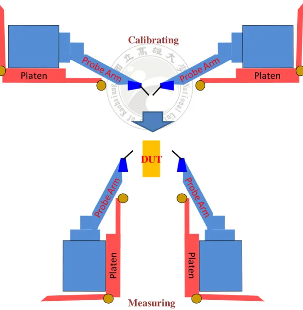
(10) Chapter 1 Introduction 1.1 Motivation Recently, the dimension of mobile devices is smaller and smaller; however the operation speed of it is higher and higher, up to several gigabits. These requirements today for every circuits and components are speeding up higher level system integration, to reducing the dimension and transmission delay. System in packaging (SIP) is a popular solution [1-6], which includes high density multi-functional integration and vertical interconnection in package with Through-silicon via (TSV). Following are several significant challenges, first that simultaneous switching noise (SSN) and signal integrity (SI) issues will occur as signal with shorter and shorter rising time transmitting from die through packaging and substrates, second that TSV technique is providing interconnection applied to stack up dies, however that signal flowing along through silicon via with high frequency propagating modes providing non-linear effects to system. Conventionally analyzing circuits with measure the RF characteristics by vector network analyzer (VNA) and RF measurement, however, this becomes a problem that RF measurement can only perform the circuits with I/O ports on the top side. In other words, highly integrated package with I/O ports on the both top and bottom sides can’t be performed directly by commonly approach [7]. The 3D integrations has been focus in 2009 international technology roadmap for semiconductors winter conference proceedings [8], this integration contains integrated passive device, test equipment, interconnect and packaging, also addressed the challenges of design and analyze. Novel double-side calibration and measurement are strongly required for system 1 .
(11) integration [9]. The key part of double-side calibration is thru element which connects RF probes with short delay time. Several approaches realizing the double-side thru element had been mentioned in industry, using via or flexible tape [10] to connect probes at the above and below side of thru element, however the discontinue effects of via and right angle with flexible tape could destroy the reproducibility of calibration. There is another approach to realize double-side measurement, rotating the platens after calibrating with conventional SOLT calibration elements as shown in Figure 1.1. As the arms rotated the cables are disturbed and limit the measurement bandwidth. In this research, a novel double-side thru element with dielectric-metal-dielectric structure is presented which remains coplanar waveguide from conventional thru element to perform very well reproducibility and broadband calibration. In the future this novel double-side thru structure can be applied to right angle double-side thru and full four port double-side calibrations.. 1.2 Thesis Organization In chapter 2, the SOLT calibration is presented which is a popular approach performing broadband calibration. Then the conventional thru calibration element is introduced and delivering the delay time by 3D EM simulation results to prove correct simulation setting. Depending on this simulation setting the novel double-side thru calibration element is developed. Finally the novel double-side calibration flow is achieved with SOLT method also the measurement equipment is presented. In chapter 3 and 4, two DUT are verifying the capability of novel double-side calibration with comparing modeling methodology and simulation. First the spring probe in Auto Testing Equipment (ATE) which has been analyzed with conventional 2 .
(12) modeling method and novel double-side measurement. It’s hoped to perform the characteristic of pogo pin directly for optimizing bandwidth of pogo pin interface in ATE. Second the trace on the substrate of package, which contains seven vias and transmit from the top metal to the bottom metal of 3-2-3 stacked up substrate. Comparing double-side measurement and SIwave simulation results is presented in chapter 4. In chapter 5, all work of this research will be summarized and the future work will be presented.. Calibrating. DUT. Measuring Figure 1.1 A diagram of developed double-side measurement 3 .
(13) Chapter 2 Calibration Calibration is the hardest work of on-wafer measurement flow, shifting the reference plane from the front of instruments to tips of probes. Calibration includes several calibration elements and complex algorithm to de-embedding the error terms of Vector Network Analyzer (VNA) [11]. The most commonly used calibration method is Short-Open-Load-Thru calibration (SOLT) [12], also this research based on, which is available on virtually every VNA and performing reasonably well because the accurate models of calibration standards can be determined, however, the disadvantages of SOLT are all standards of cal elements must be well-known and sensitive to probe placement.. 2.1 SOLT Calibration Calibration procedure is necessary for RF measurement instruments to achieve accurate measurements. Calibration de-embeds imperfections of testing equipments by measuring known quantities which are called standards. The RF characteristics of the standard are well-known beforehand. These imperfections can be isolated, quantified and mathematically removed by the standards mounted in place of the DUT. The errors of RF measurement equipments are classified two types, random and systematic. Random errors occur irregularly and unpredictably during the measurement. First the performance of semiconductor components inside test systems could vibrate easily with varying room temperature. Second the noise comes from dirty adaptors or poor connection between VNA, cable, adaptors and probes. The reduction of random measurement errors will improve by warm up equipments before measurement, operate in thermal equilibrium to avoid thermal drift and tighten the connection using torque wrench. On the other hand, systematic errors are easier to identify but cover a broadband influence. For example, the cables inherently exhibit inductance and bias tees capacitance 4 .
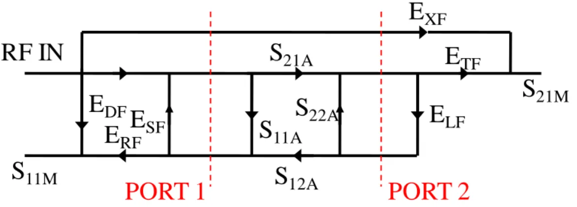
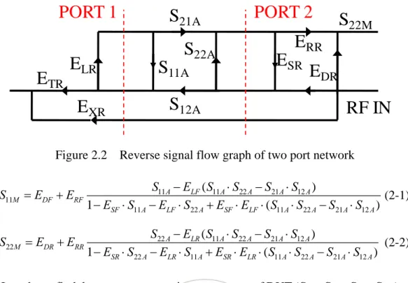
(14) at high frequency, and the dirty adaptors lead to poor connections. When the RF errors are measured repeatedly and predictably, they classify as systematic error. In most situations, both random and systematic errors occur at the same time. Compares two types of errors, the systematic errors are more significant and easier to be corrected by calibration. For a two port network, the signal flow graph is presented in Figure 2.1 and 2.2, there are separate into forward and reverse signal flow graph. Forward flow graph is presented in Figure 2.1, it contains six error terms. First directivity error, EDF, comes from the directional coupler inside test port, imperfect of directional coupler make signal couple to measure terminal before signal transmit to DUT. Source match error, ESR, presents the multi reflection between mismatched source and DUT. Reflection tracking error, ERF, represents the signal loss during reflected signal from DUT to measure terminal. Load match error (ELF) occurs as port 2 mismatch, the signal through DUT to port2 and reflects return port 1. Transmission tracking error (ETF) represents the leakage as signal transmits from port 1 to port 2. Last isolation error (EXF) represents the couple between port1 and port 2. The reverse signal flow is image of forward signal flow graph. The signal flow is analysis with Mason’s law, the return loss of port 1 before calibration, S11M, is presented in Equation 2.1, S22M in reverse obtain similarly in Equation 2.2.. EXF RF IN. S21A EDF E ERF SF. S11M. PORT 1. S22A. S11A. S12A. ETF ELF PORT 2. Figure 2.1 Forward signal flow graph of two port network 5 . S21M.
(15) PORT 1. ETR. PORT 2. S21A S22A. ELR. S11A. ERR. ESR. EDR. S12A. EXR. S22M. RF IN. Figure 2.2 Reverse signal flow graph of two port network. S11M = EDF + ERF. S11 A − ELF ( S11A ⋅ S22 A − S21 A ⋅ S12 A ) (2-1) 1 − ESF ⋅ S11 A − ELF ⋅ S22 A + ESF ⋅ ELF ⋅ ( S11 A ⋅ S22 A − S21A ⋅ S12 A ). S22 M = EDR + ERR. S22 A − ELR ( S11 A ⋅ S22 A − S21A ⋅ S12 A ) (2-2) 1 − ESR ⋅ S22 A − ELR ⋅ S11 A + ESR ⋅ ELR ⋅ ( S11A ⋅ S22 A − S21A ⋅ S12 A ). In order to find the accuracy scattering parameters of DUT (S11A, S22A, S21A, S12A), each error term must be well known by mount calibration elements one-at-a-time at test port. Consider only one port measurement first; mount load calibration element with S21A and S12A equal to zero. Port 1 and port 2 are individual impedance matched which lead to S11A and S22A equal to zero. The EDF and EDR are delivered in following:. EDF = S11MLoad. (2-3). EDR = S22MLoad. (2-4). Mounting open and short calibration elements repeatedly can obtain a set of simultaneous equations.. S11MOpen = EDF + ERF. S11MShort = EDF + ERF. S11 AOpen. (2-5). 1 − ESF ⋅ S11 AOpen. S11 AShort 1 − ESF ⋅ S11 AShort. (2-6). 6 .
(16) Here the S11AOpen and S11AShort are well known characteristics of open and short calibration elements. Then find the expressions of ERF and ESF by solving the set of simultaneous equations. − EDF + S11MOpen. ERF = ( (. S11 AOpen. +. ( EDF ⋅ S11 AOpen − S11 AOpen ⋅ S11MOpen ) S112 AOpen ⋅ S11 AShort ⋅ ( S11MOpen − S11MShort ). )⋅. (2-7). (− EDF ⋅ S11 AOpen + EDF ⋅ S11 AShort − S11 AShort ⋅ S11MOpen + S11 AOpen ⋅ S11MShort ) S112 AOpen ⋅ S11 AShort ⋅ ( S11MOpen − S11MShort ). ESF = −. ). − E DF ⋅ S11 AOpen + EDF ⋅ S11 AShort − S11 AShort ⋅ S11MOpen + ⋅S11MShort. (2-8). S11 AOpen ⋅ S11 AShort ⋅ ( S11MOpen − S11MShort ). Another set of simultaneous equations given by mounting open and short calibration elements at port 2.. S 22 MOpen = EDF + ERF. S22 MShort = EDF + ERF. S 22 AOpen. (2-9). 1 − ESF ⋅ S 22 AOpen. S22 AShort 1 − ESF ⋅ S22 AShort. (2-10). The expression of ERR and ESR is in following: ERR = ( (. − EDR + S22 MOpen. (E. S. S 22 AOpen. +. ⋅ S22 AOpen − S22 AOpen ⋅ S22 MOpen ). DR 2 22 AOpen. ⋅ S22 AShort ⋅ ( S 22 MOpen − S 22 MShort ). )⋅. (− EDR ⋅ S 22 AOpen + EDR ⋅ S 22 AShort − S22 AShort ⋅ S22 MOpen + S22 AOpen ⋅ S22 MShort ). ESR = −. 2 S 22 AOpen ⋅ S 22 AShort ⋅ ( S 22 MOpen − S 22 MShort ). − EDR ⋅ S 22 AOpen + EDR ⋅ S 22 AShort − S 22 AShort ⋅ S 22 MOpen + ⋅S 22 MShort S 22 AOpen ⋅ S 22 AShort ⋅ ( S 22 MOpen − S 22 MShort ) 7 . . (2-11) ). (2-12).
(17) After single port calibrations are done, doing thru calibrating to deliver remaining error terms. Notice the assumption that there is no DUT exist but connect two ports directly during thru calibrating in SOLT. Transfer and simplify Equation 2-1, 2-2 to find expressions of ELF and ELR with S11AThru and S22AThru are equal to zero; S21AThru and S12AThru are equal to one.. ELF =. ( S11MThr − EDF ) ESF ( S11MThru − EDF ) + ERF. (2-13). ELR =. ( S22 MThr − EDR ) ESF ( S22 MThru − EDR ) + ERR. (2-14). Finally the error terms relate to thru element is delivering, ETF, ETR, EXF and EXR. The expressions of two port measurement are following:. S21M = E XF + ETF. S21 A 1 − ESF ⋅ S11 A − ELF ⋅ S22 A + ESF ⋅ ELF ( S11 A ⋅ S22 A − S21 A ⋅ S12 A ). (2-15). S12 M = EXR + ETR. S12 A 1 − ESR ⋅ S22 A − ELR ⋅ S11A + ESR ⋅ ELR ( S11A ⋅ S22 A − S21A ⋅ S12 A ). (2-16). The EXF and EXR will be obtained as S21A and S12A equal to zero, that means each port connects load calibration element.. S21MLoad = EXF. (2-17). S12MLoad = EXR. (2-18). The expressions of ETF and ETR is delivered by taking Equation 2-17, 2-18 into 2-15 and 2-16, simplified with assumptions of S21AThru, S12AThru equal to one and S11AThru, S22AThru equal to zero.. ETF = ( S21MThru − EXF )(1 − ESF ⋅ ELF ). (2-19). 8 .
(18) ETR = ( S12 MThru − EXR )(1 − ESR ⋅ ELR ). (2-20). So far all error terms delivered, take all terms into Equation 2-15 and 2-16 to find real performance of DUT. At this time S21A and S12A are changed into S21ADUT and S12ADUT to represent DUT. Notice that some terms in denominators of Equation 2-15 and 2-16 are too little to consider.. S21 ADUT =. S21MDUT − EXF ETF. (2-21). S12 ADUT =. S12 MDUT − E XR ETR. (2-22). Take Equation 2-21, 2-22 back into Equation 2-1 and 2-2 to find S11ADUT and S22ADUT, notice the simplifying with the same assumption.. S11 ADUT =. S11MDUT − EDF − ELF ⋅ S21 ADUT ⋅ S12 ADUT ERF. (2-23). S22 ADUT =. S22 MDUT − EDR − ELR ⋅ S21 ADUT ⋅ S12 ADUT ERR. (2-24). 9 .
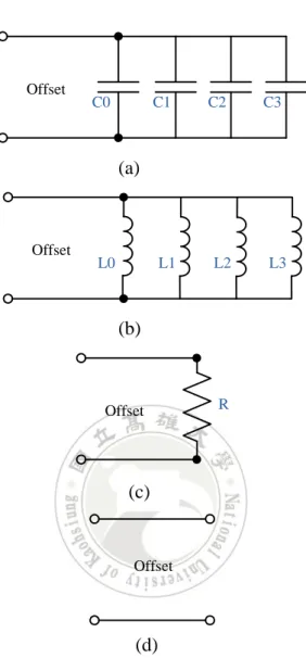
(19) 2.2 Standard Definitions All error terms are de-embedded at above section, and these well known calibration elements are represented in standard definitions. In on-wafer RF measurement, standard definitions developed from RF probe but not Impedance Standard Substrate (ISS). Because of the following reasons: 1. there are many different types of RF probe, each type with differential probe tips pitch leads to variable capacitance at open standard, also variable inductance at short standard. 2. Over-travel is the continued downward vertical movement of the probe after the device has been contacted by the probe tip. The range of over-travel is defined by probe supplier to control the contact well of probe tip. However, different over-travel of several suppliers changes the delay time of thru standard[13]. Here is an example table shows standard definitions in Table 2.1. Standard definitions must be input into VNA before calibration. Each standard describes a specific equivalent model. Open standard in Figure 2.3(a) includes parallel capacitors, which each capacitance depends on the number of power to frequency, leads to the order of C0, C1, C2 and C3 are -15, -27, -36 and -45 respectively. Every standard contains offset section, which represents the additional transmission line allows signal propagate to specific standard. For short standard, each capacitor in open model changes into inductor with the same order. Offset parameters are commonly include for load and thru standard in the on-wafer measurement. For thru standard, delay time is the most important parameter, which represents the transmission time from port 1 to port 2, then shift the calibration plane to the middle of thru line. For load standard, some supplier may not show the delay time of load standard, but give Lterm. The delay time is given by Equation 2-25.. 10 .
(20) Delay =. Lterm Z0. (2-25). Offset. C0. C1. C2. C3. (a). Offset. L0. L1. L2. L3. (b). Offset. R. (c). Offset. (d) Figure 2.3 Models of (a) open (b) short (c) load (d) thru standard definitions. . . 11 .
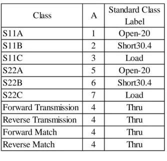
(21) Table 2.1 Example of Standard Definitions STANDARD. OFFSET FREQUENCY(GHz) TERMINAL C1 C2 C3 FIXED OR COAX OR STANDARD C0 4 LOSS IMPEDANCE DELAY Z0 - 15 - 27 -36 - 45 LOWER UPPER WAVEGUIDE LABEL *10 F *10 F/Hz *10 F/Hz *10 F/Hz SLIDING Ω GΩ/s Ω ps. NO.. TYPE. 1. Open. -20. 0. 50. 0. 0. 999. COAX. Open-20. 2. Short. 30.4. 0. 50. 0. 0. 999. COAX. Short30.4. 3. Load. 0.09. 500. 0. 0. 999. COAX. Load. 4. Thru. 1. 50. 0. 0. 999. COAX. Thru. 5. Open. -20. 0. 50. 0. 0. 999. COAX . Open-20. 6. Short. 30.4. 0. 50. 0. 0. 999. COAX . Short30.4. 7. Load. 0.09. 500. 0. 0. 999. COAX . Load. Fixed. Fixed. . . 12 .
(22) Table 2.2 Example of standard class assignments Class. A. S11A S11B S11C S22A S22B S22C Forward Transmission Reverse Transmission Forward Match Reverse Match. 1 2 3 5 6 7 4 4 4 4. Standard Class Label Open-20 Short30.4 Load Open-20 Short30.4 Load Thru Thru Thru Thru. Table 2.2 shows an example of standard class assignments. This table describes single or two port calibration at specific port with specific standard. S11A represents single port calibration at port 1 with No. 1 open standard, in other words, the different standard applied to different port are available. Even for thru standard, straight and right angle thru are available for specific couple of ports.. 13 .
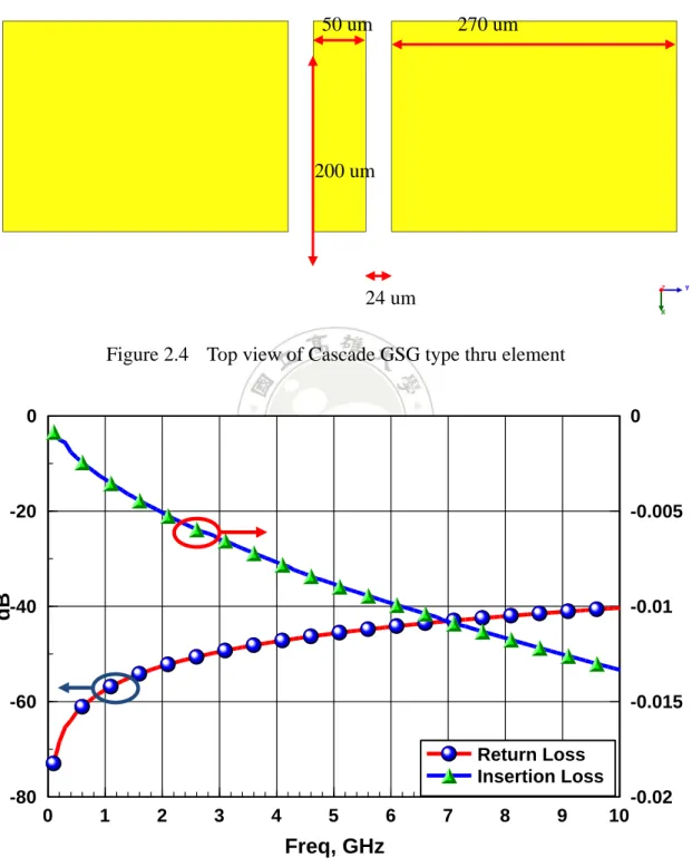
(23) 2.3 Thru Calibration Element 2.3.1 Conventional Thru Calibration element and Simulation Thru calibration element manufactured by microwave on-wafer equipment suppliers is precisely controlled the delay time. In order to design and control thru delay exactly by 3-D EM simulation, create 3-D model of conventional thru element in EM tool to verify simulation setup. The top view of GSG type thru element from Cascade is presented in Figure 2.4. This contains a CPW on 625 um thickness alumina 99.6% substrate with dielectric constant 9.0, the width of trace is 50 um, and spacing is 24 um. The definition of relationship given by Cascade is 1 ps delay per 130 um length. In this case, 200um length CPW substrates overtravel 35 um of each probe equal to 130 um, exactly 1 ps delay. In order to calculate the delay time from thru element simulation, now deliver the expression of delay time beginning from Equation 2-26[14].. θ = βl. (2-26). Which. β=. ω. (2-27). vp. Take Equation 2-27 into Equation 2-26 to find delay.. θ=. ω vp. l = ω ⋅ Delay. (2-28). Here that θ is electrical length and equal to arg(S21) in simulation, then changing the unit of electrical length from radians to degree and assuming initial phase delay of S21 is zero. Expression of delay time from simulation results is presented in Equation 2-29. 14 .
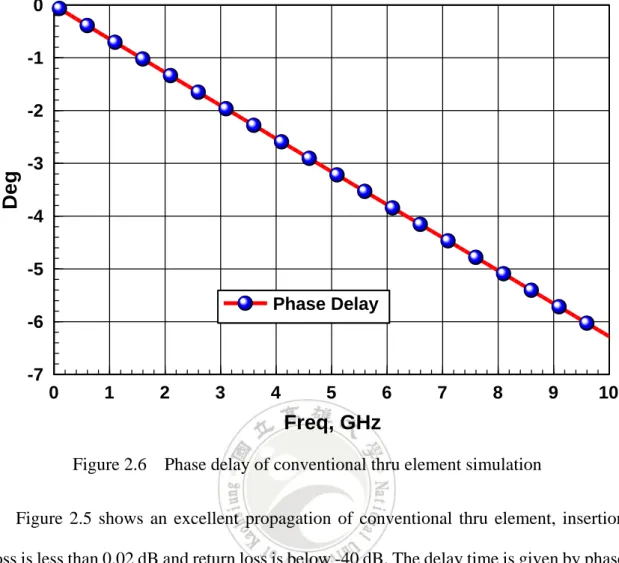
(24) Delay =. arg( S21 ( f )) − arg( S21 (0 Hz )) 360 ⋅ f. (2-29). 50 um. 270 um. 200 um. 24 um Figure 2.4 Top view of Cascade GSG type thru element 0. 0. -0.005. dB. -20. -40. -0.01. -60. -0.015 Return Loss Insertion Loss. -80. -0.02 0. 1. 2. 3. 4. 5. 6. 7. 8. 9. 10. Freq, GHz Figure 2.5 Return loss and insertion loss of conventional thru element simulation. 15 .
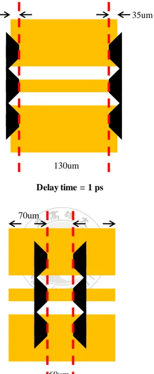
(25) 0 -1. Deg. -2 -3 -4 -5 Phase Delay -6 -7 0. 1. 2. 3. 4. 5. 6. 7. 8. 9. 10. Freq, GHz Figure 2.6 Phase delay of conventional thru element simulation Figure 2.5 shows an excellent propagation of conventional thru element, insertion loss is less than 0.02 dB and return loss is below -40 dB. The delay time is given by phase delay in Figure 2.6, usually consider the phase delay is -0.646 degree at 1 GHz, this is equal to 1.77 pico second. Then normalize this delay time from 200 um length to 130 um because of the exciting ports in simulation tool is placed on the edge of CPW. The effective delay time is 1.16 pico second which is not too far from definition 1 pico second per 130 um by Cascade. This vibration may cause by inaccuracy of lump port in EM solver. The probing placements on the thru element are controlling effective delay time. An over-travel defined by Cascade is 35 um which presents 1 pico second delay per 130 um length of thru element as shown in Figure 2.7.. 16 .
(26) 35um. 130um Delay time = 1 ps 70um. 60um Delay time = 0.46 ps Figure 2.7 Over-travel relates to delay time of thru element. 17 .
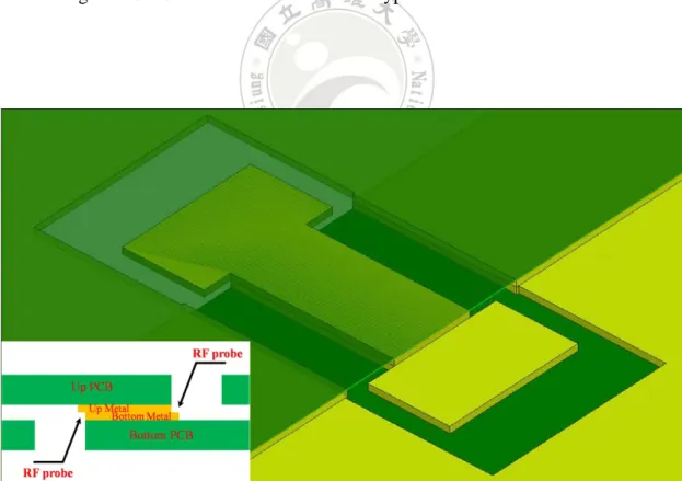
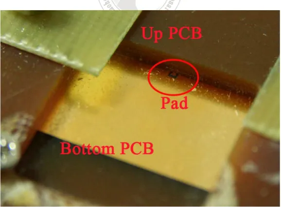
(27) 2.3.2 Novel Double-side Calibration Element and Simulation For modify this traditional thru standard into novel double-side thru standard, adding another dielectric layer at upper side of metal, each dielectric layer has been opened individually with two 50 um length slots for probing. In Figure 2.8, the cross section of embedded type double-side thru element is presented because the single layer metal is embedded into dielectric layer. The spacing between signal and ground metal is changed from 23 into 63 um to control impedance 50 Ohm with two dielectric layer, but the impedance of probing areas are 68 Ohm on only one dielectric layer. This impedance mismatch leads to energy reflect, therefore, the pad exposed to air is changed into 90 um width and 40 spacing. However, it’s difficult for process to manufacture this embedded type novel double-side thru element because that opening windows must be achieved by buried via, which using laser to burn partial dielectric and the planarity must be controlled well. Another structure that allows double-side probing with easier manufacture process is presented in Figure 2.9. This cross type double-side thru element contains two separate PCB stacked face-to-face with each PCB slotted to expose copper layer for the probing. Each PCB has been etched like Figure 2.10. There is a 0.75 mm length, 250um width, and 155 um spacing for the CPW transmission line on each PCB with 2 mm thick Nelco N4000 dielectric and the thickness of each single copper layer is 20 um. By combining the two PCBs together, they become a 0.5mm 50 ohm CPW line embedded in dielectrics with two opposite-oriented 0.25 mm pads exposed to the air as shown in Figure 2.11. There are two issues that involve impedance control and adhesion between the two PCBs that must be taken care of. The width and spacing of the exposed pad is 425 and 75 um. The difference between conventional and the novel double-side thru element approach is that it contains two dielectric layers and embeds the CPW. The manufactured sample of 18 .
(28) double-side cross type element is presented in Figure 2.11.. Figure 2.8 Cross section of embedded type double-side thru element. Figure 2.9 Cross section of cross type double-side thru element. 19 .
(29) Overlap. Slot. Figure 2.10 Pattern of each PCB of cross type double-side thru element. Figure 2.11 Photo of cross type double-side thru element 20 .
(30) Notice that the ground plane is surround the signal trace and unit two piece of ground besides signal trace, this design allows different type and pitch of probe to achieve SOLT calibration, for example GSG-GS, GSG-SG, GS-GS and GS-SG types. Of cause, the thru delay will change as different match up. Table 2.3 shows the thru delay of several matches up. Table 2.3 Delay time of different matches up Delay. GS-550. SG-550. GSG-550. GS-550. 10.14 ps. 9.2 ps. 8.39 ps. SG-550. 9.2 ps. 10.14 ps. 8.39. GSG-550. 8.39. 8.39. 7.2 ps. 21 .
(31) 2.4 Novel Double-side Calibration Flow and Measurement Equipment Before processing novel double-side calibration, the most important thing is making RF probes aim to opposite direction. A customized probe station is showed in Figure 2.12, which rotate the arm to place the probe below DUT and make probe tip upward as shown in Figure 2.13. Compares conventional on-wafer calibration and novel double-side calibration, the thru standard have to be modified which depends on what type of probes matched up, as mentioned above. Here is an example with Agilent E5071C:. z. Press “cal” button.. z. Press “calibration element” and select the standard corresponding to the probe.. z. Select “modify standard”, and get into thru standard.. z. Change the “delay” into delay time of double-side thru element.. In this thesis, all measurement results are depend on Cascade ACP-40-SG-550 and ACP-40-GS-550 probe, which corresponds to 106-683 impedance standard substrate.. 22 .
(32) Figure 2.12 Photo of customized probe station. Figure 2.13 Photo of double-side probing. 23 .
(33) 2.5 Double-side Calibration Results In this section, reconnect all calibration elements to verify the accuracy of calibration is presented. First problem shows that each part of customized probe station with slight shaking leads to cable sway, that’s why the vibration of port 2 response to calibration results. First reconnect open calibration element which presents raising up probe more than 0.2 mm. The return loss of open standard at port 1 and 2 are presented in Figure 2.14, the return loss of port 1 is perfect, and the slight vibration at port 2 is still in specifications of within plus or minus 0.02 dB. The phase of open standard at port 1 and 2 are presented in Figure 2.15, they are matched and arise from 0 deg, also show capacitances of open standard. Second reconnect short calibration element, which is a metal plane connect signal and ground tips of each probe. In Figure 2.16, both return loss of short at port 1 and 2 are perfect, also in Figure 2.17 that phase decrease from 180 deg. Third reconnect load calibration element and the return loss is presented in Figure 2.18, they almost below -40 dB for whole band. At last reconnect double-side thru calibration element, the cable swaying affects insertion loss of thru standard much as shown in Figure 2.19; however, they are very close to the specifications of within plus and minus 0.02 dB. The phase delay in Figure 2.20 is 3.662 deg at 1 GHz, which equals to 10.172 pico second delay, and this is matched to GS-SG type matched up in Table 2.3.. . 24 .
(34) 0.06. dB (Ruturn Loss). 0.04. 0.02. 0. -0.02. -0.04 port 1 port 2 -0.06 0. 2. 4. 6. 8. 10. 12. 14. 16. 18. 20. Freq, GHz Figure 2.14 Return loss of the open standard after calibration 5 4.5 4. deg (phase). 3.5 3 2.5 2 1.5 1 port 1 port 2. 0.5 0 0. 2. 4. 6. 8. 10. 12. 14. 16. Freq, GHz Figure 2.15 Phase of the open standard after calibration 25 . 18. 20.
(35) 0.06. dB (Return Loss). 0.04. 0.02. 0. -0.02. -0.04 port 1 port 2 -0.06 0. 2. 4. 6. 8. 10. 12. 14. 16. 18. 20. Freq, GHz Figure 2.16 Return loss of the short standard after calibration 180. deg (phase). 178. 176. 174. 172. 170 port 1 port 2 168 0. 2. 4. 6. 8. 10. 12. 14. 16. Freq, GHz Figure 2.17 Phase of the short standard after calibration 26 . 18. 20.
(36) 0. dB (Return Loss). -20. -40. -60. -80 port 1 port 2 -100 0. 2. 4. 6. 8. 10. 12. 14. 16. 18. 20. Freq, GHz Figure 2.18 Return loss of the load standard after calibration 0.06. dB (Insertion Loss). 0.04. 0.02. 0. -0.02. -0.04 thru_S12 thru_S21 -0.06 0. 2. 4. 6. 8. 10. 12. 14. 16. Freq, GHz Figure 2.19 Insertion loss of the thru standard after calibration 27 . 18. 20.
(37) 0. deg (Phase Delay). -10 -20 -30 -40 -50 -60 -70. thru_S12 thru_S21. -80 0. 2. 4. 6. 8. 10. 12. 14. 16. Freq, GHz Figure 2.20 Phase delay of the thru standard after calibration. 28 . 18. 20.
(38) Chapter 3 Introduction and Analysis of Spring Probe. Increasingly high-speed serial I/Os are available in mobile products operating at gigabit data rates, creating significant challenges not only for silicon providers, but also for the Automated Testing Equipment (ATE) industry. The ATE provides a methodology for transmitting signals to and from the device under test (DUT) to the tester. The critical challenge is maintaining the signal integrity between the ATE instruments and the DUT. The spring probe type assemblies have been a standard interface in the ATE industry, consisting of an adjustable length spring applied to the spring probe that ensures a good connection. The electromagnetic coupling between each pin creates crosstalk noise and a repeatedly pressed spring is unstable. Previously studies have discussed the impedance and delay time of several spring probe types [15], and novel high-speed and ultra high speed spring probe types have been used [16-18]. Subsequently, the crosstalk noise between spring probes has become the most critical signal integrity issue for high-speed digital systems. Enlarging the pin pitch of spring probe structures reduces crosstalk noise. The current advanced systems with high-density pads do not have this capability. We seek to increase the bandwidth of the spring probe interface. The modeling method presented in following is complex and imprecise. The characteristic performance of the spring probe requires many fixtures to achieve the open and short at the terminal of spring probe that creates and de-embeds the equivalent model attaining real performance of the spring probe [19-21]. The parasitic effect of fixtures could be larger than spring probe in most cases and the ground loop inductance has been ignored when shorting the terminals of spring probes and results in the distortion of an equivalent model. 29 .
(39) The distortion of the equivalent model isn’t only appearing on spring probe but also every vertical transmission structure, because the de-embedded method will become a challenge when DUT is smaller than the effects of fixture and ground inductance can’t be precisely detected. The reliability of spring probe interface is also a significant issue, when tester lay down DUT quickly and repeatedly to compress spring probes, pins inside socket could skew, damaged [22] or compressed not enough to working length, finally fails the testing. In this research, a novel microwave on-wafer double-side measurement technology has been developed to performing the real effect of spring probe, and compared with traditional modeling method. For spring probe type assemblies, this novel measurement approach may not improve a lot, but it presents the ability to become a critical solution for coming signal integrity issues like TSV and 3DIC.. 30 .
(40) 3.1 Spring Probe Configuration and Modeling The RF spring probes characteristics have been performed with load boards or test fixtures from the ATE industry. The response of the whole structure is obtained by this approach. The real characteristic of spring probe section only cannot be obtained, because of de-embedding of transmission lines, adaptors, and vias. The approach used creates the schematic equivalent model by curve fitting several test fixtures. A modeling method that includes complex mathematical operations and model optimization is presented. Notice that test fixtures with parasitical effects will limit the bandwidth of an equivalent model. The modeling method is presented below. The whole structure is presented in Figure 3.1 and is divided into three parts. The PCB board represents the adapter between RF probe and spring probe for probing space and transmitting signals into spring probes with vias as shown in Figure 3.2. Next is the spring probe. The test board allows the terminals of spring probes to become an open or short circuit. These three parts are similar and simplified into two signal paths port 1- port 3 and port 2 - port 4. Each path contains a series of main inductors (Li, Lj) and two external inductors (Lipcb, Ljpcb; Litb, Ljtb), the lossy components and mutual inductances have been considered for every inductor and for the electrical coupling between the two paths. Coupling between signal path and ground are considered parallel capacitors. This model can be applied to both differential modes and single-end transmissions. The single-end mode is considered one signal pin and one ground pin and will be grounded at port 2 and port 4.. 31 .
(41) Figure 3.1 Basic equivalent model of spring probe and fixtures. (a). (b). Figure 3.2 (a) Spring probe side of text fixture (b) RF probing side of test fixture. Consideration of each cell in the model as shown in Figure 3.3a. The first opened is port 3, while port 4 delivers only one port response. This model can be simplified into two parallel capacitors at a low frequency. All lossy components will be considered at the 32 .
(42) final stage of this modeling method. The S11 with an open path is presented in Equation 3-1. Notice that port 2 is terminated at this time.. op S11 =. 1 − jωZ 0 (Ci + Cij ) 1 + jωZ 0 (Ci + Cij ). =. 1 − [ωZ 0 (Ci + Cij )]2 1 + [ωZ 0 (Ci + Cij )]. 2. −j. 2ωZ 0 (Ci + Cij ) 1 + [ωZ 0 (Ci + Cij )]2. (a). (3-1). (b). Figure 3.3 (a) Simplified model with open path (b) Simplified model with short path The calculation, Equation 3-1 is changed into following equation. op tan(−∠S11 )=. 2ωZ 0 (Ci + Cij ). (3-2). 1 − [ωZ 0 (Ci + Cij )]2. The second term of denominator in Equation 3-2 is less than 1, because the unit of Ci and Cij are pico-farad, ω is giga Hz. Equation 3-2 can be simplified into Equation 3-3 when the second term of denominator is ignored. op tan(−∠S11 ) = 2ωZ 0 (Ci + Cij ). (3-3). The expression of Ci and Cj can be found in Equation 3-4, 3-5. Ci =. op tan( −∠S11 ) − Cij 2ωZ 0. (3-4). 33 .
(43) Cj =. op tan(−∠S 22 ) − Cij 2ωZ 0. (3-5). Consider the effects between ports 1 and 2, the model at low frequency can be simplified into Cij that connects the two ports. Delivering the ABCD matrix of Cij and changes into a scattering matrix. The S12 with the open path is shown in Equation 3-6.. op = S12. 2 jωZ0Cij 1 + 2 jωZ0Cij. =. 4ω 2 Z 02Cij2 1 + 4ω. 2. Z02Cij2. +j. 2ωZ 0Cij 1 + 4ω 2 Z02Cij2. (3-6). The expression of Cij is delivered in Equation 3-7. 2. op S12 1 Cij = 4πfZ 0 1 − S op 12. (3-7). 2. The previous model in Figure 3-3b shows the short path at ports 3 and 4 occur at external inductances which Lw and Lg. Lw suited to the wire bonding to ground at the package level modeling, and Lg represents ground inductance of the short path. Conventionally Lw and Lg are ignored and assumed the sampling at low frequency. This assumption limits the model’s bandwidth. The conductive silver paste has been coated on the probing side of test board to achieve a short path and combine parasitical effects of conductive pastes with ground inductance into Lg. Repeatedly terminating port 2 to show S11 in the simplified model at low frequency and deliver Li and Lj.. sp S11. 2 2 Z in − Z 0 ω ( Li + Lg ) − Z 0 + 2 jω ( Li + Lg ) Z 0 = = Z in + Z 0 ω 2 ( Li + Lg ) 2 + Z 02. (3-8). Equation 3-8 is changed into 3-9 for calculation. sp tan(∠S11 )=. 2ω ( Li + Lg ) Z 0. (3-9). ω 2 ( Li + Lg ) − Z 02. 34 .
(44) sp tan(∠S11 ) sp 1 + sec(∠S11 ). =. 2ω ( Li + Lg ) Z 0. (3-10). 2ω 2 ( Li + Lg ) 2. Li and Lj are found in the following: Li =. sp ) Z 0 1 + sec(∠S11 − Lg sp 2πf tan(∠S11 ). (3-11). Lj =. sp ) Z 0 1 + sec(∠S 22 − Lg sp 2πf tan(∠S 22 ). (3-12). Delivering the mutual inductance between Li and Lj has been replaced by T model and simplified to the series of Lij and Lg. sp S 21 =. 4ω 2 ( Lij + L g ) 2 + 2 jω ( Lij + Lg ) Z 0 2 = Z0 Z 02 + 4ω 2 ( Lij + Lg ) 2 2+ jω ( Lij + Lg ). (3-13). Finally the mutual inductance is delivered in Equation 3-14. Lij =. Z 0 sp S − Lg 2ω 21. (3-14). Most components of the cell model in Figure 3.3 have been delivered by remaining lossy with capacitors obtained by optimizing the model in EDA tools that fit the measurement data. The disadvantages of this modeling method are the characteristics of PCB and fixtures must know in order to be de-embedded from the whole model indicated by Figure 3.1. The characteristics of spring probes through simulation instead of measurements. PCB and test board are similar and perform the same modeling steps mentioned above. . 35 .
(45) Table 3.1 Parameters of whole model. Cij. 57.456 fF. Cijpcb, Cijtb. 5.728 fF. Ci, Cj. 90 fF. Cipcb, Cjpcb, Citb, Cjtb. 140 fF. Lij. 0.858nH. Lijpcb, Lijtb. 0.02 nH. Li. 1.8 nH. Lipcb, Litb,. 0.27 nH. Lj. 1.8 nH. Ljpcb, Ljtb. 0.18 nH. Mutual K. 0.477. Mutual Kpcb, Ktb. 0.077. . 36 .
(46) 3.2 Measurement Results of Spring Probe and Discussion Configuration of measuring spring probes with double-side probe station is shown in Figure 3.4. The spring probe structure shown in Figure 3.5 shows the position of one signal pin and another ground pin with pitch of 0.8 mm. The two configurations must tighten all screws on the fixture and loosen two screws beside the spring probes, see the highlight in Figure 3.2(b). This represents each time compressing spring probe to working length and indicates a compression error. The comparisons between the novel 3D direct measurement and conventional modeling method are presented in Figures 3.6, 3.7 and 3.8. The measurements of the models are similar, but a comparison shows parasitical effects that the models did not capture after 3.6 GHz. This error arises from the inaccuracy inductance of the conductive silver paste on the ground path which brings transmission drop down at higher frequency in Figure 3.6 and 3.7. This mismatch could be worsened if Lg is ignored as the modeling flow. Notice that there are reliability issues by compress error that wrong probe length leads to poor contact and impedance discontinue performing the resonance frequency early.. Figure 3.4 Configuration of measuring spring probes with double-side probe station. 37 .
(47) Figure 3.5 Detail structure of spring probes. 0. dB (Insertion Loss). -1. -2. -3. -4 tighten pins by double-side mea. equivalent model loose pins by double-side mea.. -5. -6 0. 1. 2. 3. 4. 5. 6. Freq, GHz Figure 3.6 Insertion loss of modeling, 3D measured tighten and loosen spring probes. 38 .
(48) 0. dB (Return Loss). -10. -20. -30. tighten pins by double-side mea. equivalent model loose pins by double-side mea.. -40. -50 0. 1. 2. 3. 4. 5. 6. Freq, GHz Figure 3.7 Return loss of modeling, 3D measured tighten and loosen spring probes 0. deg (Phase Delay). -20. -40. -60. -80. equivalent model tighten pins by double-side mea. loose pins by double-side mea.. -100 0. 1. 2. 3. 4. 5. 6. Freq, GHz Figure 3.8 Phase delay of modeling, 3D measured tighten and loosen spring probes 39 .
(49) Chapter 4 Introduction and Analysis of Trace on Package Substrate. 4.1 Introduction of Trace on Package Substrate A substrate of popular high density BGA package as shown in Figure 4.1 carry the die and fan out the input and output of die to the backside of substrate, mounting the packaging on a main board. There are numerous traces on the substrate which transmit signal from the die side to broad side with vias. Figure 4.1 and 4.2 point the probing placements at the front and back side with cascade GS-550 probe, Figure 4.3 highlights the trace characterized by novel double-side measurement which on the top metal layer. As trace transmit signal to the bottom metal layer as shown in Figure 4.4, it through seven vias. The cross section of trace is presented in Figure 4.5, includes six 35 um length and one 800 um length via.. Gnd. Signal. Figure 4.1 Probing at the front side of substrate. 40 .
(50) Gnd. Signal. Figure 4.2 Probing at the back side of substrate. Via. Gnd. Signal Figure 4.3 Top metal of substrate. 41 .
(51) Gnd Signal. Figure 4.4 Bottom metal of substrate. Figure 4.5 Cross section of trace with vias 42 .
(52) 4.2 Discussion and Comparison of Simulation and Measurement Results Comparing SIwave simulation results and novel double-side measurement results by as shown in following. In SIwave, the whole substrate layout has been simulated instead of clip a part of substrate. The reference ground of trace is placed on the second metal layer and it’s scrappy around through hole. It may effects the return path at reference ground if second metal layer has been clipped. The return loss of the front and the backside is realized and displayed separately in Figure 4.6 and 4.7. Insertion loss is presented as shown in Figure 4.8. Double-side measurement results is almost matched to SIwave simulation results and perform each zero and pole precisely before 10 GHz, especially the excellent agreement of phase delay as shown in Figure 4.9. The phase delay directly relates to propagating constant which easily causing nonlinear phase delay as discontinue. The phase delay measured by double-side measurement remains straight shows better reliability than simulated nonlinear phase delay.. 43 .
(53) 0. Return Loss (dB). -5 -10 -15 -20 -25 -30 -35. Double-side measured at front side Siwave simulation at front side. -40 0. 2. 4. 6. 8. 10. 12. 14. 16. 18. 20. Freq, GHz Figure 4.6 Return loss of measurement and simulation at front side 0. Return Loss (dB). -5 -10 -15 -20 -25 -30 -35. Double-side measured at backside Siwave simulation at backside. -40 0. 2. 4. 6. 8. 10. 12. 14. 16. 18. Freq (GHz) Figure 4.7 Return loss of measurement and simulation at backside 44 . 20.
(54) 0. Insertion Loss (dB). -2 -4 -6 -8. -10 -12. Double-side measured Siwave simulation. -14 0. 2. 4. 6. 8. 10. 12. 14. 16. 18. 20. Freq (GHz) Figure 4.8 Insertion loss of measurement and simulation 200. Double-side measured Siwave simulation. Phase Delay (deg). 150 100 50 0 -50. -100 -150 -200 0. 2. 4. 6. 8. 10. 12. 14. 16. Freq (GHz) Figure 4.9 Phase delay of measurement and simulation 45 . 18. 20.
(55) Chapter 5 Conclusion and Future Work. In this research, the novel double-side calibration and measurement are developed and been well verified by comparing conventional modeling method of spring probe and simulation results of package substrate. The novel double-side thru element manufacture without via avoids parasitical effects and easily realizes. Reconnect each standard after calibration presents the reliability of novel double-side calibration and measurement as shown in section 2.5, the all measured results are meet specifications. This is an important proof about the capability of novel double-side calibration and measurement. Novel double-side calibration and measurement performs DUT with vertical signal path accurately, quickly and simply. In chapter 3, an accuracy measurement result is presented without complex methodology. In chapter 4, a trace with several vias is easily characterized by double-side measurement and performing excellent agreements with SIwave simulation results. In the future, the most important thing is developing fine pitch match up wide pitch calibration and double-side right angle thru element. Therefore, this novel double-side calibration and measurement can fully applied to 3D package, no matter interconnection of die stacked up, whole package of system and auto testing equipments.. . 46 .
(56) Reference [1]. [2]. [3] [4] [5] [6] [7] [8]. [9] [10]. [11] [12]. [13] [14] [15]. S. W. Yoon, V. P. Ganesh, S. Y. L. Lim, and V. Kripesh, "Packaging and assembly of 3-D silicon stacked module for image sensor application," IEEE Transactions on Advanced Packaging, vol. 31, pp. 519-526, Aug 2008. H. Yamada, T. Togasaki, M. Kimura, and H. Sudo, "High-density 3D packaging sidewall interconnection technology for CCD micro-camera visual inspection system," Electronics and Communications in Japan Part II-Electronics, vol. 86, pp. 67-75, 2003. S. K. Lim, "Physical design for 3D system on package," Design & Test of Computers, IEEE, vol. 22, pp. 532-539, 2005. B. C. Kim and Y. Zorian, "Guest Editors' Introduction: Big Innovations in Small Packages," Design & Test of Computers, IEEE, vol. 23, pp. 186-187, 2006. M. Kada, "The dawn of 3D packaging as system-in-package (SIP)," in IEICE Transactions on Electronics, 2001, pp. 1763-1770. S. Sapatnekar and K. Nowka, "Guest Editors' Introduction: New Dimensions in 3D Integration," Design & Test of Computers, IEEE, vol. 22, pp. 496-497, 2005. E. J. Marinissen and Y. Zorian, "Testing 3D chips containing through-silicon vias," in International Test Conference, 2009. L. Wei-Chung, C. Yu-Hua, K. Cheng-Ta, and K. Ming-Ger, "TSV and 3D wafer bonding technologies for advanced stacking system and application at ITRI," in 2009 Symposium on VLSI Technology, 2009, pp. 70-71. H. H. S. Lee and K. Chakrabarty, "Test Challenges for 3D Integrated Circuits," Design & Test of Computers, IEEE, vol. 26, pp. 26-35, 2009. Sung-Mao Wu and C.-T. Chiu, "Impedance Standard Substrate and Correction Method for Vector Network Analyzer," Advanced Semiconductor Engineering, Inc., Kaohsiung (TW), 2006. V. Adamian, "Simplified Automatic Calibration of a Vector Network Analyzer (VNA)," in ARFTG Conference Digest-Fall, 44th, 1994. W. Kruppa and K. F. Sodomsky, "An Explicit Solution for the Scattering Parameters of a Linear Two-Port Measured with an Imperfect Test Set (Correspondence)," IEEE Transactions on Microwave Theory and Techniques, vol. 19, pp. 122-123, 1971. S. Wartenberg, RF measurements of die and packages: Artech House Publishers, 2002. M. Hiebel, Fundamentals of vector network analysis: Rohde&Schwarz, 2007. C. Ming-Kun, T. Cheng-Chi, H. Yu-Jung, and F. Li-Kuei, "Electrical characterization of BGA test socket for high-speed applications," in 2002. 47 . .
(57) [16]. [17]. [18]. [19]. [20]. [21]. [22]. Proceedings of the 4th International Symposium on Electronic Materials and Packaging, 2002, pp. 123-126. H. Barnes, J. Moreira, H. Ossoinig, M. Wollitzer, T. Schmid, and T. Ming, "Development of a pogo pin assembly and via design for multi-gigabit interfaces on automated test equipment," in Proceedings of Asia-Pacific Microwave Conference, 2006, pp. 381-384. B. B. Szendrenyi, H. Barnes, J. Moreira, M. Wollitzer, T. Schmid, and T. Ming, "Addressing the Broadband Crosstalk Challenges of Pogo Pin Type Interfaces for High-Density High-Speed Digital Applications," in IEEE/MTT-S International Microwave Symposium, 2007, pp. 2209-2212. S. Ruey-Bo, W. Chang-Yi, C. Yen-Chih, and W. Ruey-Beei, "A new isolation structure for crosstalk reduction of pogo pins in a test socket," in 2009. IEEE 18th Conference on Electrical Performance of Electronic Packaging and Systems, 2009, pp. 227-230. S. Ruey-Bo, W. Ruey-Beei, and H. Shih-Wei, "Compromised impedance match design for signal integrity of pogo pins structures with different signal-ground patterns," in 2009. IEEE Workshop on Signal Propagation on Interconnects, 2009, pp. 1-4. T. S. Horng, S. M. Wu, H. H. Huang, C. T. Chiu, and C. P. Hung, "Modeling and evaluating leadframe CSPs for RFICs in wireless applications," in 2001. Proceedings., 51st Electronic Components and Technology Conference, 2001, pp. 348-352. T. S. Horng, S. M. Wu, and C. Shih, "Electrical modeling of RFIC packages up to 12 GHz," in 1999. Proceedings of the 49th Electronic Components and Technology Conference, 1999, pp. 867-872. T. Hsien-Chiao, C. Ming-Kun, Y. Chia-Hao, H. Yu-Jung, and F. Shen-Li, "Study of contact degradation in final testing for BGA socket," in International Conference on Electronic Materials and Packaging 2007.. 48 .
(58) Appendix Appendix A. Double-side Calibration Flow. 49 .
(59) Appendix B. Introduction of Instruments. Customized Probe Station. Agilent ENA E5071C 50 .
(60)
數據
+7
相關文件
The Centre for Learning Sciences and Technologies (CLST), The Chinese University of Hong Kong (CUHK) launched the!. EduVenture ® learning system, which has been well received by
1INTRODUCTION DuyMinhDang ChristinaC.Christara Adaptiveandhigh-ordermethodsforvaluingAmericanoptions
Furthermore, by comparing the results of the European and American pricing prob- lems, we note that the accuracies of the adaptive finite difference, adaptive QSC and nonuniform
Biases in Pricing Continuously Monitored Options with Monte Carlo (continued).. • If all of the sampled prices are below the barrier, this sample path pays max(S(t n ) −
Although the research of problem-based learning (PBL) and the integration of PBL and Zuvio IRS in Japanese pedagogy are trending, no related research has been found in Japanese
According to the simulation results, the sliding distances and the contact forces are the almost same on the upper and lower layers probe for the models of single pitch, ten
Through the analysis of Structural Equation Modeling (SEM), the results of this research discover that the personal and family factors, organizational climate factors,
Carrying on the analysis by the expert fuzzy Delphi method regarding this investigation results, the research seeks and induces the most suitable weight of the leading behavior
In this Research, the Analytic Hierarchy Process and Case Study Method are used, from which three main factors affecting the work progress were obtained: “Encountering of
