ECS Journal of Solid State Science and Technology, 2 (9) N179-N181 (2013) N179 2162-8769/2013/2(9)/N179/3/$31.00©The Electrochemical Society
Low Operation Voltage InGaZnO Thin Film Transistors with
LaAlO
3Gate Dielectric Incorporation
Z. W. Zheng,a,zC. H. Cheng,band Y. C. Chenc
aInstitute of Microelectronics, Chinese Academy of Sciences, Beijing 100029, China
bDepartment of Mechatronic Technology, National Taiwan Normal University, Taipei 106, Taiwan cInstitute of Photonic System, National Chiao Tung University, Hsinchu 300, Taiwan
In this paper, we report low operation voltage indium gallium zinc oxide (IGZO) thin film transistors (TFTs) incorporating a high-κ lanthanum aluminum oxide (LaAlO3) as gate dielectric. Good TFT characteristics were achieved simultaneously, including a small subthreshold swing (SS) of 98 mV/dec, a low threshold voltage (Vt) of 0.29 V, a good on-off-state drive current ratio (Ion/Ioff) of 1.1× 10⁵, and field effect mobility (μFE) of 5.4 cm2/V· sec. These good performances are related to the high gate capacitance density and small equivalent oxide thickness (EOT) provided by the high-κ LaAlO3dielectric. Moreover, the effects of oxygen partial pressure during IGZO deposition process on the device characteristics were investigated. The small SS and low Vtallow the devices to be used at operation voltage as low as 1.5 V, which shows the great potential for future high speed and low power applications. © 2013 The Electrochemical Society. [DOI:10.1149/2.020309jss] All rights reserved.
Manuscript submitted May 6, 2013; revised manuscript received June 3, 2013. Published July 6, 2013.
With the rapid development of active-matrix flat panel displays (AMFPDs), thin film transistor (TFT) technologies have been widely used for display applications. However, the traditional Si TFTs using amorphous silicon and poly-crystalline silicon as active channel layer face difficulties due to physical drawback properties.1–3Recently, the
new TFTs with transparent oxide semiconductors have attracted much attention as potential candidates, due to their unique optical and elec-trical advantages as compared to conventional Si TFTs, such as high mobility, low cost, excellent uniformity, and good transparency to vis-ible light.4–25Particularly, indium gallium zinc oxide (IGZO) TFT7–25
with superior stability and performance is one of the most promising candidates and has been widely studied. Moreover, the IGZO TFTs can be processed with very low thermal budget and used in emerging flexible display applications.
With the above merits of IGZO film, the IGZO TFT devices are being considered for a variety of applications, such as low-cost large-area displays, RFIDs and wearable electronics.7,8For high-speed
dis-play circuits, it requires TFTs to operate at low voltages and high drive currents with low threshold voltage (Vt) and small subthreshold swing (SS), which make low operation voltage TFTs very favorable for efficiency improvement and environment energy conservation. To address these concerns, incorporating high-κ gate dielectric into TFT provides an alternative solution to achieve these goals.26–28 In this
paper, we report a low operation voltage IGZO TFT by introducing a high-κ lanthanum aluminum oxide (LaAlO3)28–30as gate dielectric.
Due to the higherκ-value (∼23) of LaAlO3 dielectric as compared to that of SiO2(∼3.9), the gate capacitance density increases, which lowers the Vt and improves the gate leakage current. Besides, the LaAlO3dielectric has good reliability of low bias temperature insta-bility among high-κ devices. The LaAlO3TFTs showed a small SS of 98 mV/dec, a low Vtof 0.29 V, good on-off-state drive current ratio (Ion/Ioff) of 1.1× 10⁵, and field effect mobility (μFE) of 5.4 cm2/V· sec at the operation voltage as low as 1.5 V. Furthermore, the influences of oxygen partial pressure during IGZO film deposition process on the device characteristics were investigated, since IGZO has electrons as majority carriers, which is mainly affected by the oxygen vacancies.31
The present results demonstrate that IGZO TFTs with high-κ LaAlO3 as gate dielectric has great promise in future high speed and low power applications.
Experimental
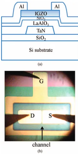
Figure1aand1bshow the schematic cross-sectional structure and microscopic image of the IGZO TFT device, respectively. The channel width (W) and length (L) of the TFTs were 500μm and 50 μm, respectively. Bottom-gate top-contact IGZO TFTs were fabricated on
zE-mail:[email protected]
an insulated SiO2/Si substrate through a four-shadow-mask process flow. Firstly, a 50 nm TaN was deposited by physical vapor deposition (PVD) and patterned as gate (G) electrode. Next, a 30 nm LaAlO3and a 10 nm SiO2were deposited by PVD as gate dielectrics, followed by a 400◦C O2annealing to improve the gate oxide quality. Sequentially, a 40 nm IGZO was formed as active channel layer by dc reactive sputtering using an IGZO target with a power of 80 W and an oxygen partial pressure of PO2= 50% in Ar and O2mixed gas ambient under a working pressure of 7.6 mTorr at room temperature. Here, oxygen partial pressure of PO2 (%) is defined as the mixing ratio of O2 / (O2 + Ar). Finally, Al source (S)/drain (D) electrodes of 300 nm
Figure 1. (a) Schematic cross-sectional structure and (b) microscopic image
of the IGZO TFT device with LaAlO3gate dielectric incorporation.
) unless CC License in place (see abstract).
ecsdl.org/site/terms_use
address. Redistribution subject to ECS terms of use (see
140.113.38.11
N180 ECS Journal of Solid State Science and Technology, 2 (9) N179-N181 (2013)
were deposited, followed by sintering at 300◦C in N2 ambient to reduce the contact resistance. The control samples of IGZO/LaAlO3 TFT without SiO2layer insertion were fabricated for comparison. To further evaluate the effects of oxygen partial pressure during IGZO deposition on the device characteristics, the TFT devices with PO2of 33% and 0% in IGZO deposition were also fabricated. The metal-insulator-metal (MIM) capacitors were also fabricated to investigate gate dielectric. The TFT devices were characterized by current-voltage (I-V) and capacitance-voltage (C-V) measurements using HP4156C semiconductor parameter analyzer.
Results and Discussion
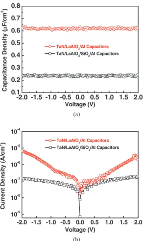
Figure 2a and 2b show the C-V and J-V characteristics of the TaN/LaAlO3/Al and TaN/LaAlO3/SiO2/Al gate capacitors on the same substrate, respectively. The high capacitance density of
∼0.62 μF/cm2 and ∼0.23 μF/cm2 was measured for the
TaN/LaAlO3/Al and TaN/LaAlO3/SiO2/Al MIM capacitors, respec-tively. It indicates an equivalent oxide thickness (EOT) of∼5.5 nm and ∼15 nm for single LaAlO3and bilayer LaAlO3/SiO2gate dielectrics, respectively, giving a highκ-value of ∼21–23 in the LaAlO3 dielec-tric. Such large gate capacitance density can give the advantages of lowering the operation voltage, increasing the transistor drive cur-rent, and improving the Ion/Ioff. Besides, the large gate leakage of 6.9 × 10⁻⁶ A/cm2 at −2 V bias was significantly decreased to 1.5× 10⁻⁷A/cm2 after the insertion of SiO2layer. This SiO2layer evaporated at room temperature without sputtering plasma damage can effectively reduce interface state near the IGZO active channel layer.23,24
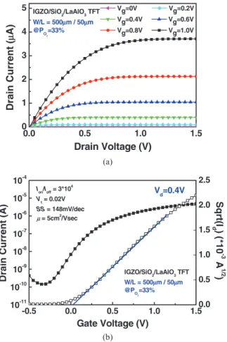
The output Id-Vd characteristics of the IGZO/SiO2/LaAlO3 TFT when PO2 = 50% are shown in Figure3a. An enhancement-mode
-2.0 -1.5 -1.0 -0.5 0.0 0.5 1.0 1.5 2.0 0.1 0.2 0.3 0.4 0.5 0.6 0.7 0.8 Capacit ance Density ( µ F/cm 2 ) Voltage (V) TaN/LaAlO3/Al Capacitors
TaN/LaAlO
3/SiO2/Al Capacitors
(a) -2.0 -1.5 -1.0 -0.5 0.0 0.5 1.0 1.5 2.0 10-9 10-8 10-7 10-6 10-5 10-4 Curren t Density (A/cm 2 ) Voltage (V) TaN/LaAlO3/Al Capacitors
TaN/LaAlO3/SiO2/Al Capacitors
(b)
Figure 2. (a) C-V and (b) J-V characteristics of the TaN/LaAlO3/Al and
TaN/LaAlO3/SiO2/Al gate capacitors fabricated on the same substrate.
0.0 0.5 1.0 1.5 0 1 2 3 Drain Current ( µ A) Drain Voltage (V) Vg=0V Vg=0.2V Vg=0.4V Vg=0.6V Vg=0.8V Vg=1.0V IGZO/SiO2/LaAlO3 TFT W/L = 500µm / 50µm @PO 2 =50% (a) -0.5 0.0 0.5 1.0 1.5 10-11 10-10 10-9 10-8 10-7 10-6 10-5 10-4 Ion/Ioff = 1.4*103 Vt = 0.41V SS = 390mV/dec µ = 1.3cm2 /Vsec
Drain Current (A)
Gate Voltage (V) 0.0 0.5 1.0 1.5 2.0 2.5 IGZO/LaAlO3 TFT IGZO/SiO2/LaAlO3 TFT W/L = 500µm / 50µm @PO 2 =50% Ion/Ioff = 1.1*105 Vt = 0.29V SS = 98mV/dec µ = 5.4cm2 /Vsec Vd=0.4V Sqrt(I d) (*10 -3 A 1/2 ) (b)
Figure 3. (a) Output Id-Vdcharacteristics and (b) transfer Id-Vgcharacteristics of the IGZO/LaAlO3and IGZO/SiO2/LaAlO3TFTs when PO2= 50%.
behavior with good saturation characteristics was well observed even under an operation voltage as low as 1.5 V, which could enable energy saving for low power application. Figure 3b displays the transfer
Id-Vg characteristics of the IGZO/LaAlO3 and IGZO/SiO2/LaAlO3 TFTs when PO2= 50% for a Vdof 0.4 V, along with the Id1/2versus Vg plot. For the TFT device characteristics, Vtcan be determined from the linear Id1/2-Vgcurve and Ion/Ioffcan be obtained from the Id-Vgcurve. Besides,μFEcan be extracted from a gradual channel approximation in the linear region using the equation:32
μFE= ∂ Id/∂Vg· L/(W · Vd· Cg), [1]
where Id, Vd, Vg, L, W, and Cgare the drain current, drain voltage, gate voltage, channel length, channel width, and gate insulator capacitance per unit area, respectively. For the IGZO/LaAlO3TFT device, it shows a Vtof 0.41 V and a low operation voltage of 1.5 V, but suffers a low
Ion/Ioffof 1.4× 10³, a smallμFEof 1.3 cm2/V· sec and a large SS of 390 mV/dec. In contrast, the IGZO/SiO2/LaAlO3TFT device exhibits a much largerμFEof 5.4 cm2/V· sec and a higher Ion/Ioffof 1.1× 10⁵ due to small gate leakage current, with a Vtof 0.29 V. Besides, a much smaller SS of 98 mV/dec is achieved in the IGZO/SiO2/LaAlO3TFT device and closed to the theoretical minimum value of 60 mV/dec at room temperature, indicating the device can be switched on fast at very low operation voltage. These good performances can be attributed to the insertion of SiO2 layer, which is necessary for stable operation of TFT devices.23,24,33 By introducing smooth SiO2 layer insertion,
the high-κ surface can be passivated and the interface trap issue can be effectively reduced, thus the performances can be improved, as reported in the literatures.23,24
To further investigate the influences of oxygen partial pressure during IGZO deposition process, the IGZO/SiO2/LaAlO3 TFT de-vice characteristics with the IGZO active channel layers deposited at different oxygen partial pressure (PO2= 0% and PO2= 33%) were
) unless CC License in place (see abstract).
ecsdl.org/site/terms_use
address. Redistribution subject to ECS terms of use (see
140.113.38.11
ECS Journal of Solid State Science and Technology, 2 (9) N179-N181 (2013) N181 0.0 0.5 1.0 1.5 0 1 2 3 4 5 IGZO/SiO 2/LaAlO3 TFT W/L = 500µm / 50µm @PO2=33% Drain Current ( µ A) Drain Voltage (V) Vg=0V Vg=0.2V Vg=0.4V Vg=0.6V Vg=0.8V Vg=1.0V (a) -0.5 0.0 0.5 1.0 1.5 10-11 10-10 10-9 10-8 10-7 10-6 10-5 10-4
Drain Current (A)
Gate Voltage (V) V d=0.4V 0.0 0.5 1.0 1.5 2.0 2.5 IGZO/SiO2/LaAlO3 TFT W/L = 500µm / 50µm @P O2=33% Sqrt(I d ) (*10 -3 A 1/ 2 ) Ion/Ioff = 3*104 Vt = 0.02V SS = 148mV/dec µ = 5cm2 /Vsec (b)
Figure 4. (a) Output Id-Vdcharacteristics and (b) transfer Id-Vgcharacteristics of the IGZO/SiO2/LaAlO3TFT when PO2= 33%.
compared to the characteristics of TFT device when PO2 = 50%. It is well-known that the carrier concentration and the mobility of sputtered IGZO film can be controlling by the mixing ratio of sput-tering gases during deposition process.25Defects created by the ion
bombardments and incorporation of sputtering ions act as scattering centers or charge traps for the carriers, and thus degrade the electrical device performances.17 For the PO2 = 0% TFT device, it behaved
with failed transistor characteristics with large leakage current (not shown). For the PO2= 33% TFT device, the output Id-Vdand trans-fer Id-Vgcharacteristics are shown in Figure4aand4b, respectively. As compared to the TFT device when PO2= 50%, the PO2= 33% TFT device exhibits degraded performances, including a much lower
Ion/Ioff of 3× 10⁴ and a smallerμFE of 5 cm2/V· sec, and a much larger SS of 148 mV/dec with a Vt of 0.02 V. It can be attributed to the oxygen partial pressure when depositing the IGZO film as the active channel layer. Since the IGZO film has electrons as majority carriers, which is mainly affected by the oxygen vacancies during deposition process.31When the IGZO film is deposited at low PO2
= 0%, the oxygen is not supplied sufficiently, causing the increase of oxygen vacancies, which may act as shallow donors.34In this case,
the active IGZO film would have a relatively high carrier density and behave with conducting property. This may be one of the reasons why the TFT using IGZO film when PO2= 0% exhibited failed transistor characteristics with large leakage current. However, with the increase of PO2when depositing the IGZO film, the amount of the oxygen va-cancies decrease, leading to the decrease of carrier density, and thus the IGZO electrical property may change from conducting to insu-lating via semiconducting. It agrees with the improved TFT device characteristics when increasing the PO2from 0% to 50% during the active IGZO channel layer deposition process.
Conclusions
In conclusion, incorporating a high-κ LaAlO3 as gate dielectric, the IGZO TFTs show a small SS of 98 mV/dec, a low Vt of 0.29 V, a good Ion/Ioffof 1.1× 10⁵, and an acceptableμFEof 5.4 cm2/V· sec at operation voltage as low as 1.5 V. These good performances were related to the high gate capacitance density and small EOT by in-troducing the high-κ LaAlO3dielectric. Furthermore, with relatively high oxygen partial pressure during IGZO deposition process, the TFT device characteristics could be improved due to the low oxygen vacancy formation. The present results show that these low operation voltage IGZO TFTs with high-κ LaAlO3as gate dielectric have high potential for future high speed and low power applications.
Acknowledgment
The authors thank Professor Albert Chin in National Chiao Tung University, Hsinchu, Taiwan, for his support and technical help on experiments.
References
1. C. W. Chen, T. C. Chang, P. T. Liu, H. Y. Lu, K. C. Wang, C. S. Huang, C. C. Ling, and T. Y. Tseng,IEEE Electron Device Lett., 26, 731 (2005).
2. K. M. Chang, W. C. Yang, and C. P. Tsai,IEEE Electron Device Lett., 24, 512 (2003). 3. C. H. Tseng, T. K. Chang, F. T. Chu, J. M. Shieh, B. T. Dai, H. C. Cheng, and A. Chin,
IEEE Electron Device Lett., 23, 333 (2002).
4. R. L. Hoffman, B. J. Norris, and J. F. Wager,Appl. Phys. Lett., 82, 733 (2003). 5. B. Yaglioglu, H. Y. Yeom, R. Beresford, and D. C. Paine,Appl. Phys. Lett., 89,
062103 (2006).
6. N. L. Dehuff, E. S. Kettenring, D. Hong, H. Q. Chiang, J. F. Wager, R. L. Hoffman, C. H. Park, and D. A. Keszler,J. Appl. Phys., 97, 064505 (2005).
7. K. Nomura, H. Ohta, A. Takagi, T. Kamiya, M. Hirano, and H. Hosono,Nature, 432, 488 (2004).
8. E. Fortunato, P. Barquinha, and R. Martins,Adv. Mater., 24, 2945 (2012). 9. N. C. Su, S. J. Wang, and A. Chin,IEEE Electron Device Lett., 30, 1317 (2009). 10. A. Sato, M. Shimada, K. Abe, R. Hayashi, H. Kumomi, K. Nomura, T. Kamiya,
M. Hirano, and H. Hosono,Thin Solid Films, 518, 1309 (2009).
11. J. S. Park, T. W. Kim, D. Stryakhilev, J. S. Lee, S. G. An, Y. S. Pyo, D. B. Lee, Y. G. Mo, D. U. Jin, and H. K. Chung,Appl. Phys. Lett., 95, 013503 (2009). 12. J. Y. Kwon, K. S. Son, J. S. Jung, T. S. Kim, M. K. Ryu, K. B. Park, B. W. Yoo,
J. W. Kim, Y. G. Lee, K. C. Park, S. Y. Lee, and J. M. Kim,IEEE Electron Device Lett., 29, 1309 (2008).
13. P. Barquinha, L. Pereira, G. Goncalves, R. Martins, and E. Fortunato,J. Electrochem. Soc., 156, H161 (2009).
14. A. Suresh, P. Wellenius, and J. F. Muth, inIEDM Tech. Dig., 587 (2007). 15. P. Barquinha, A. M. Vila, G. Goncalves, L. Pereira, R. Martins, J. R. Morante, and
E. Fortunato,IEEE Trans. Electron Devices, 55, 954 (2008).
16. J. B. Kim, C. Fuentes-Hernandez, and B. Kippelen,Appl. Phys. Lett., 93, 242111 (2008).
17. H. Yabuta, M. Sano, K. Abe, T. Aiba, T. Den, H. Kumomi, K. Nomura, T. Kamiya, and H. Hosono,Appl. Phys. Lett., 89, 112123 (2006).
18. S. Y. Huang, T. C. Chang, M. C. Chen, S. W. Tsao, S. C. Chen, C. T. Tsai, and H. P. Lo,Solid-State Electronics, 61, 96 (2011).
19. H. S. Uhm, S. H. Lee, W. Kim, and J. S. Park,IEEE Electron Device Lett., 33, 543 (2012).
20. N. C. Su, S. J. Wang, C. C. Huang, Y. H. Chen, H. Y. Huang, C. K. Chiang, and A. Chin,IEEE Electron Device Lett., 31, 680 (2010).
21. W. Lin, J. H. Jang, S. H. Kim, D. P. Norton, V. Craciun, S. J. Pearton, F. Ren, and H. Shen,Appl. Phys. Lett., 93, 082102 (2008).
22. J. C. Park and H. N. Lee,IEEE Electron Device Lett., 33, 818 (2012). 23. M. Kitamura and Y. Arakawa,Appl. Phys. Lett., 89, 223525 (2006).
24. J. H. Na, M. Kitamura, D. Lee, and Y. Arakawa,Appl. Phys. Lett., 90, 163514 (2007). 25. J. H. Na, M. Kitamura, and Y. Arakawa,Appl. Phys. Lett., 93, 063501 (2008). 26. M. F. Chang, P. T. Lee, S. P. McAlister, and A. Chin,IEEE Electron Device Lett., 29,
215 (2008).
27. M. F. Chang, P. T. Lee, S. P. McAlister, and A. Chin,IEEE Electron Device Lett., 30, 133 (2009).
28. B. F. Hung, K. C. Chiang, C. C. Huang, A. Chin, and S. P. McAlister,IEEE Electron Device Lett., 26, 384 (2005).
29. D. S. Yu, K. C. Chiang, C. F. Cheng, A. Chin, C. Zhu, M. F. Li, and D. L. Kwong,
IEEE Electron Device Lett., 25, 559 (2004).
30. D. S. Yu, A. Chin, C. C. Laio, C. F. Lee, C. F. Cheng, W. J. Chen, C. Zhu, M. F. Li, W. J. Yoo, S. P. McAlister, and D. L. Kwong, inIEDM Tech. Dig., 181 (2004).
31. H. Omura, H. Kumomi, K. Nomura, T. Kamiya, M. Hirano, and H. Hosono,J. Appl. Phys., 105, 093712 (2009).
32. S. M. Sze and K. K. Ng, Physics of Semiconductor Devices, 3rd ed., p. 308, John Wiley & Sons, New Jersey (2007).
33. G. Wang, D. Moses, A. J. Heeger, H. M. Zhang, M. Narasimhan, and R. E. Demaray,
J. Appl. Phys., 95, 316 (2004).
34. A. Janotti and C. G. Van de Walle,Phys. Rev. B, 76, 165202 (2007).
) unless CC License in place (see abstract).
ecsdl.org/site/terms_use
address. Redistribution subject to ECS terms of use (see
140.113.38.11