Low-Power Wordline Voltage Generator
for Low-Voltage Flash Memory
Tzu-Ming Wang1, Ming-Dou Ker1, Steve Yeh2, and Ya-Chun Chang2
1Nanoelectronics and Gigascale Systems Laboratory
Institute of Electronics, National Chiao-Tung University Hsinchu, Taiwan
2NVM Product R&D Division
Winbond Electronics Corporation Science-Based Industrial Park
Hsinchu, Taiwan
Abstract—Wordline voltage generating circuit with high speed
active mode and low power standby mode is proposed. In the active mode, two different ring oscillators with high clock frequency (fCLK) 170MHz, and low clock frequency (fCLK) 25MHz which is also the operating frequency of the entire circuit, are employed. The proposed circuit has a short response time of 3µs typically in active mode, and very low
standby current about 3µA in standby mode.
I. INTRODUCTION
Recently, flash memories are in widespread applications especially in many portable products, such as cellular phones, palm-top computers, and so on. For most of portable products, power consumption is an important issue needed to be concerned because a long battery life is an extreme merit. To reduce the power consumption, the simplest and most efficient way is to reduce its power supply voltage [1]. However, too low power supply voltage degrades circuit performance. For example, speed, dynamic range, and noise margin are affected. For flash memory applications, the high voltage operation in programming, erasing, or reading is also difficult to achieve with low power supply voltage. So, the voltage boosting circuit is used to boost power supply voltage to higher voltage level as required.
Two ways used mostly in voltage boosting circuits are Dickson charge pump [2] and capacitor-switched booster circuit [3]. The Dickson charge pump takes advantage of lower power, smaller chip area, and fast access time while suffering from the standby current compared with capacitor-switched booster circuit [3]. To reduce the average current in the standby mode is a crucial issue when Dickson charge pump is used as voltage boosting circuit. In [4], the wordline voltage generating circuit for low-power and low-voltage flash memories had been proposed to provide a good architecture and solution to reduce the standby current of Dickson charge pump in the standby mode. In case of the resistive load is connected to the output in active mode, the response time increases on account of the finite load current. The response time is defined by the time when output voltage varies from 0V to its specified steady state voltage.
Fig. 1. Block diagram of the conventional wordline generating circuit [4].
Fig. 2. Dickson charge pump circuit with a resistive load [6].
Since the active mode with resistive load needs longer response time to achieve steady state of the entire system, there are many analyses to discuss this issue [5]-[7]. In this paper, the wordline voltage generating circuit with low power in standby mode and short response time in active mode is proposed.
II. CONVENTIONAL WORDLINE GENERATING CIRCUIT
Fig. 1 illustrates the block diagram of the conventional wordline generating circuit [4]. The resistive load (RL) is
only connected to the output in the active mode. Ideally, the active charge pump is designed to boost supply voltage to the specified output voltage (VOUT), which may be above or
below the limited range in real implementation due to process variation. Consequently, the charge pump regulator scheme is needed. In [4], it utilizes the comparator and the resistor divider to compare the divided VOUT with constant
reference voltage. If the divided VOUT is greater than the
constant reference voltage, the comparator stops the ring OSC (Oscillator). When the ring oscillator stops, the charge pump stops boosting too. Therefore, the VOUT is decreased
and vice versa.
To perform the low standby current, the voltage divider requires large resistors in standby mode. With the aforementioned charge pump regulator scheme, if the time that the ring oscillator stops is longer, the circuit has a lower standby current. The larger capacitor used in the standby charge pump results in the longer time ring oscillator takes to stop. Comparatively, the large capacitor also needs large taper buffer size to charge it. In [4], a latch and a counter are used in the standby mode. Variation of power supply voltage and temperature has great influence on the average standby current consumption. The taper buffer consumes the major portion of the average standby current, and it has the correlation with the counting number of the standby ring oscillator. Therefore, the conventional wordline generating circuit utilizes a latch and a counter to control the counting number to reach optimized standby current consumption.
To decrease the response time is an important issue in a power-up state. When the circuit has a short response time, short recovery time appears after the output voltage drops suddenly [5]. Fig. 2 shows the standard Dickson charge pump with a capacitive and a resistive load connected to the output. Two out-of-phase clock signals, CLK and CLKB, boost the capacitors (C) to raise the output voltage (VOUT) to
the specified high voltage. In [6] and [7], rise time Tr can be
derived as
1) Without a resistive load:
CLK g g OUT r T V V V T × − − =
β
ln 1 ln (1) Load NC C + = 1 1 β (2)where Vg = VDD-Vt, Vt is the threshold voltage, and TCLK is
the cycle time of driving clock.
2) With a resistive load:
CLK OUT M OUT M r T V V V V T × − − =
β
ln ) 0 ( ln (3) Load Load L CLK C N C C R T × + × − = 1 1 β (4) where =(
−1+ −1)
−1 OUT p C C C ,(
)
(
)
[
]
. 8 1 and 1 1 1 1 + − × − = + × + = − − OUT OUT CLK OUT L L g M C C C R T R R R T C N V N VIn (2) and (4), CLoad = COUT + Cpump and Cpump is about NC/3.
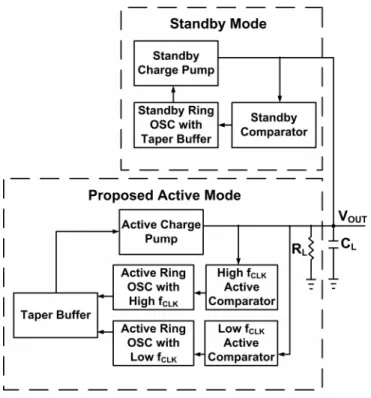
Fig. 3. New proposed wrodline generating circuit.
III. NEW PROPOSED WORDLINE GENERATING CIRCUIT
Fig. 3 shows the new proposed wordline generating circuit. In the active mode, the output has an additional resistive load (RL), and it results in the finite load current.
The increasing response time results from the finite load current. According to (1) and (3), a new active mode is proposed to reduce the response time. In the standby mode, a latch and a counter are left out.
In the active mode, two different ring oscillators with high clock frequency (fCLK) 170MHz, and low clock
frequency (fCLK) 25MHz which is also the operating
frequency of the entire circuit, are employed. Each of the two ring oscillators is controlled by different comparators. In the power-up state, the active ring oscillator with high fCLK is
used to boost active charge pump first, so the output voltage would rise more quickly than conventional wordling generating circuit with a resistive load. Before the output voltage just reaches its steady state, the high fCLK active
comparator stops high fCLK ring oscillator, but the low fCLK
active comparator starts the low fCLK ring oscillator. After the
transition between two ring oscillators, the active mode works in steady state with proper operating clock frequency 25MHz, thus it would not cause extra average current consumption. The higher clock frequency also means the smaller pumping period, and the larger current of the taper buffer is needed to boost charge pump to the specified high voltage. In other words, a large taper buffer size is inevitable. Under considerations of chip size and current consumption, the high clock frequency should not be chosen too high.
Fig. 4. Active charge pump with a diode (D) connected between VDD to
VOUT.
Fig. 4 shows the active charge pump with a diode (D) connected between VDD and VOUT. When the power-up state
begins, VOUT varies from 0V to the specified output voltage.
At the beginning of operation, the diode (D) makes VOUT
reach to VDD-Vt in advance (Vt is about 0.5V), so it leaves
out the time taking for VOUT from 0V to VDD-Vt. When VOUT
reaches to steady state output voltage (4.5V to 4.7V), the diode (D) is off without breakdown.
In the standby mode, the regulation is controlled by only the standby comparator. As mentioned before, Dickson charge pump has a finite standby current. The standby comparator decides the boosted voltage value, whether the standby ring oscillator works or not. The entire system takes the average current into account, thence the standby period which is composed of pumping and blocking period [5] should be as long as possible. Consequently, not only the capacitors used in standby charge pump should be suitable, but also the boosted voltage in the pumping period should be high enough to increase the standby period.
IV. SIMULATION RESULTS
In order to evaluate and analyze the new proposed wrodline generating circuit compared with the conventional one, the circuit with four stage charge pump, a 100kΩ resistive load and a 2nF capacitive load is performed. The output voltage should be limited from 4.5V to 4.7V. A supply voltage (VDD) is from 1.6V to 2V, the operating
frequency works at 25MHz, the high clock frequency in the active mode is 170MHz, and the temperature varies from -40oC to 85oC. The simulation uses SPICE Model in a
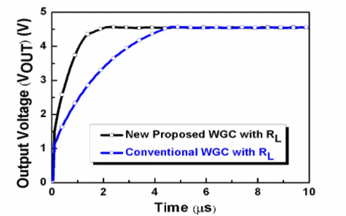
0.18µm 1.8V/5V 1P4M Logic Process with Embedded Flash. Fig. 5 shows the simulation results between the new proposed and conventional wordline generating circuit (WGC). The simulation conditions are VDD = 1.6V, RL =
100kΩ, operation clock frequency = 25MHz, temperature = 25oC, and V
OUT is not out of the specified range in steady
state (4.5V to 4.7V). In this work, RL is large enough to
bring relatively small load current, thus the response time between conventional WGC with or without RL is similar.
Nonetheless, the response time is still too long for conventional WGC. In the new proposed WGC, the response time improves obviously, as shown in Fig. 5. The response time in the new proposed WGC with RL is about 1.86µs, and
the response time is 4.34µs in the conventional WGC with the same RL. The improvement is about 57.14%.
Fig. 5. Comparisons between the new proposed and conventional wordline generating circuit (WGC) in active mode with a resistive load (RL).
Fig. 6. Two different clock frequencies (fCLK) in the active mode.
Fig.6 has the same condition with the new proposed WGC with RL in Fig. 5, but it illustrates two different clock
frequencies in the active mode. The dense waveform in clock frequency (fCLK) is high fCLK with 170MHz, and the rare
waveform is low fCLK with operation clock frequency of
25MHz. At the beginning of the active mode, high fCLK
executes. With high fCLK and the additional diode (D), the
output voltage rises rapidly. After the high fCLK stops at the
time of 1.4µs, the low fCLK starts to boost charge pump and
the output voltage (VOUT) rises smoothly. After the time of
2.2µs, fCLK holds with constant voltage level of VDD, that is,
both ring oscillators stop boosting output voltage because VOUT reaches to its steady state (4.5V to 4.7V).
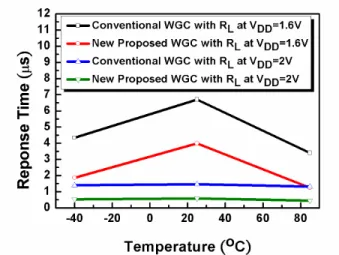
In real applications, variation of supply voltage and temperature should be cogitated. Fig.7 shows the response time with difference supply voltage and temperature. At VDD
= 1.6V, temperature of -40oC, 25oC, and 85oC are simulated.
Each of them compared with conventional WGC with RL has
improvement of 57.14%, 40.45%, and 65.53%, respectively. At VDD = 2V, the new proposed WGC with RL has
improvement of 62.3%, 59.86%, and 65.9% under the corresponding temperatures.
Fig. 7. The response time between conventional and the new proposed WGC with RL at VDD=1.6V and 2V.
Fig. 8. The average standby current at VDD=1.6V and VDD=2V.
The response time between VDD = 1.6V and 2V are quite
different in Fig. 7. In the new proposed WGC, the ring oscillator is utilized to boost the charge pump, but the frequency of ring oscillator is excessively related with supply voltage. The higher supply voltage leads to higher clock frequency. In (1) and (3), the frequency has extreme influence on the response time.
In the new proposed WGC, only a comparator is used to regulate the standby mode. The standby comparator only consumes about 100 nA, and the standby charge pump consumes about few hundred nano amp. The current consumption of the standby charge pump is decided by the resistors used in the voltage divider. The current goes through the standby comparator, and the voltage divider is very small, thus the response time of standby comparator is longer than that of active comparator. It may result in the output voltage larger than 4.7V in the pumping period of the standby mode. For this reason, the resistor value of the voltage divider and the current consumption of comparator in standby mode are required to modify.
Fig. 8 shows the simulation results of average standby current consumption. Under considerations of variation of supply voltage and temperature, output voltage is successfully controlled in the range of 4.5V to 4.7V, and current consumption is below 3.3µA. At temperature of -40oC, the circuit operation with V
DD of 1.6V and 2V have
excessive different current consumption compared with others. The standby regulator is only composed of a comparator, hence the temperature variation has more influences than conventional WGC. As mentioned before, the standby period is as long as possible if the standby current demands to be smaller. The higher output voltage level in the pumping period brings about the longer blocking period. At VDD = 1.6V and temperature = -40oC, the standby
comparator has worse performance, so the boosted voltage in the pumping period is lower than others. Therefore, the standby period is also smaller to increase the average standby current consumption.
V. CONCLUSION
A new wordline voltage generating circuit with high speed active mode and low power standby mode is proposed. The circuit has been simulated in a 0.18µm 1.8V/5V 1P4M Logic Process with Embedded Flash. In active mode, the response time has been improved from 40.45% to 65.9% in different supply voltages and temperatures. In standby mode, average standby current is from 1.56µA to 3.3µA under variations of supply voltages and temperatures. The experimental chip to verify this design is now under wafer fabrication. The measured results will be shown in the presentation.
ACKNOWLEDGMENT
The authors would like to thank the project support from Winbond Electronics Corporation with wafer fabrication.
REFERENCES
[1] G. Palumbo, D. Pappalardo, and M. Gaibotti, “Charge-pump circuits: power-consumption optimization,” IEEE Trans. Circuits Syst. I, vol. 49, pp. 1535-1542, Nov. 2002.
[2] J. F. Dickson, “On-chip high-voltage generation in NMOS integrated circuits using an improved voltage multiplier techniques,” IEEE J. Solid-State Circuits, vol. 11, pp.374-378, June, 1976.
[3] T. Tanzawa and S. Atsumi, “Optimization of word-line booster circuits for low-voltage flash memories,” IEEE J. Solid-State Circuits, vol. 34, pp. 1091-1098, Aug. 1999.
[4] T. Tanzawa A. Umezawa, M. Kuriyama, T. Taura, H. Banba, T. Miyaba, H. Shiga, Y. Takano, and S. Atsumi, “Wordline voltage generating system for low-power low-voltage flash memories,” IEEE J. Solid-State Circuits, vol. 36, pp. 55-63, Jan. 2001.
[5] J.-Y. Lee, S.-E. Kim, S.-J. Song, J.-K. Kim, S. Kim, and H.-J. Yoo, “A regulated charge pump with small ripple voltage and fast start-up,” IEEE J. Solid-State Circuits, vol. 41, pp. 425-432, Feb. 2006. [6] M. Zhang and N. Llaser, “Dynamic analysis of dickson charge pump
circuits with a resistive load,” IEEE International Conference on Electionics, Circuits and Systems, pp. 431-434, Dec. 2003.
[7] T. Tanazawa and T. Tanaka, “A dynamic analysis of the dickson charge pump circuit,” IEEE J. Solid-State Circuits, vol. 32, pp. 1231-1240, Aug. 1997.
![Fig. 2. Dickson charge pump circuit with a resistive load [6].](https://thumb-ap.123doks.com/thumbv2/9libinfo/7667893.141037/1.918.472.836.467.555/fig-dickson-charge-pump-circuit-resistive-load.webp)