國立交通大學
電子工程學系 電子研究所
博 士 論 文
n 型反置層精準量子計算:
應變、次能帶、遷移率及三維結構
Sophisticated Quantum Computation on n-type Inversion
Layers: Strain, Subband, Mobility, and 3-D Structure
研究生: 李韋漢
指導教授: 陳明哲 博士
n 型反置層精準量子計算:
應變、次能帶、遷移率及三維結構
Sophisticated Quantum Computation on n-type Inversion
Layers: Strain, Subband, Mobility, and 3-D Structure
研 究 生: 李韋漢 Wei-Han Lee
指導教授: 陳明哲 博士 Dr. Ming-Jer Chen
國立交通大學
電子工程學系 電子研究所
博士論文
A DissertationSubmitted to Department of Electronics Engineering & Institute of Electronics
College of Electrical and Computer Engineering National Chiao Tung University
in Partial Fulfillment of the Requirements for the Degree of
Doctor of Philosophy in
Electronics Engineering November 2012
Hsinchu, Taiwan, Republic of China
I
n 型反置層精準量子計算:
應變、次能帶、遷移率及三維結構
研究生: 李韋漢 指導教授: 陳明哲 博士
國立交通大學
電子工程學系 電子研究所博士班
摘要
根據莫爾定律法則,我們正走向 22/20 奈米的科技世代,而且會不停地繼續 開發更新更有效率的元件。然而在前進的路上會遇到許多問題,其中一個值得注 意的問題是應力效應,它會影響到元件的一些電性和製程上的問題。這些物理特 性我們可以從對漏電流和電子遷移率的實驗及模擬上觀察到。此外閘極穿隧電流 跟次能階高度和位能障等能帶結構有強烈的相關性。所以閘極穿隧電流是個找次 能階和應力效應的好工具。要建立一個正確的 n 型轉置層模擬計算,我們從對閘 極穿隧電流的數據去做匹配的動作,接著是遷移率的計算,最後完成一個全面性 的計算工作。 能帶結構計算和遷移率量測在最近被用來評估在場效電晶體中等效質量隨 著應變之下的變化係數。在此論文中,我們提出一個新的實驗方法,乃藉由對 <110>方向上的壓縮應變改變 (001) n 型金氧半場效電晶體的閘極直穿隧電流做 匹配動作。這個方法的重點是直穿隧的機制對在等效質量隨著應變之下的變化係 數非常敏感,因為變化係數可以影響到次能階的位置。在此,我們使用了一個以II 三角位能近似的架構的模擬器。為了達到更精確的成果,我們提出了一個修正係 數的演算法去補償使用三角位能近似法解出次能階計算上的誤差。接著用已知的 形變位能常數和單向壓縮應力作為輸入的條件,帶有應力效應的量子模擬器就完 成了。模擬器計算出的閘極直穿隧電流被用來與實驗比較,因此帶出兩谷和四谷 的等效質量隨應變下變化係數的值。其值也跟被發表在文獻的值作比較。 在我們以實驗的方法,透過應力誘發閘極穿隧電流增益,去萃取二維電子氣 的等效質量隨應變的變化係數,結果指出導帶中垂直平面方向上(量子侷限)四谷 的等效質量隨應變的變化係數是存在的。為了更確定這個事情,在此我們提供了 另一個證據。首先,我們針對幾種不同的等效質量隨應變的變化係數的值作為明 確的方針。接著,我們採用一個可計算應力和量子效應的自洽的模擬器去執行同 時對文獻上在單向拉伸應力的實驗情形下遷移率增加和閘極電流減少作個匹配。 發現在能帶計算上忽略了垂直平面方向上四谷的等效質量隨應變的變化係數只 會做出很差的匹配結果。 在模擬器結構被建立且可信之下,可使我們的工作延伸到其他情況。除了之 前的(001) 平面, (110) 和 (111) 的平面場效電晶體中次能階和遷移率的計算 也可以用以估計在應力工程下的傳輸特性。穿隧效應在元件微縮下顯得越重要。 為了要對三維結構,像是鰭狀場效電晶體的電性做些實驗,雙閘極場效電晶體結 構的次能階計算可以直接的達成。計算結果也顯示出在薄基板厚度下特別易有穿 隧效應。同樣地,在不同平面不同通道方向的元件時,應力影響遷移率的變化也 可以被估計出來。
III
Sophisticated Quantum Computation on n-type Inversion
Layers: Strain, Subband, Mobility, and 3-D Structure
Student: Wei-Han Lee Advisor: Dr. Ming-Jer Chen
Department of Electronics Engineering and Institute of Electronics
National Chiao Tung University
Abstract
Following Moore’s law, we are currently entering into the technology generation of 22/20 nm and will keep developing newer and more efficient devices. We will encounter many problems in this long road. Stress engineering is one of the noticeable candidates due to significant changes in electrical performance and process issues. By fitting to the data of leakage current and electron mobility, some physical mechanisms can be brought out. On the other hand, the gate direct tunneling correlates strongly with the band structure, such as the subband energy level and barrier height. Thus, the gate direct tunneling could be a good tool to detect the subband level and hence the effect of stress. To build a correct computation of n-inversion layer in our simulator, this work starts with the fitting to gate direct tunneling data, followed by the mobility calculation brought out in the next step and finally the comprehensive computational work.
Currently, both the band-structure calculation and the mobility measurement are used to assess the electron piezo-effective-mass coefficients in strained nMOSFETs. In this work, we present a new experimental method through a fitting of the
IV
strain-altered electron gate direct tunneling current of (001) n-channel metal–oxide–semiconductor field effect transistors under <110> uniaxial compressive stress. The core of this method lies in the sensitivity of the direct tunneling to the position of the subband level in the presence of the electron piezo-effective-mass coefficients. Here, a simulator based on triangular potential approximation is utilized. To make more accurate calculation, we proposed a new algorithm that a correction-coefficient generating expression is systematically constructed to compensate for the error in the subband levels due to the use of a triangular potential approximation. Then, with the known deformation potential constants and uniaxially compressive stress in the channel as inputs, a strain quantum simulator is carried out. The resulting gate direct tunneling current is used to fit experimental data, thus leading to the values of the piezo-effective-mass coefficients associated with the twofold and fourfold valleys. The comparison of the extracted piezo-effective-mass coefficients with those published in the literature is made.
After we have experimentally extracted the piezo-effective-mass coefficients of 2-D electrons via the stress-induced gate tunneling current enhancement, the results pointed to the existence of a piezo-effective-mass coefficient around the fourfold conduction-band valley in the out-of-plane (quantum confinement) direction. To strengthen this further, here, we provide extra evidence. First, explicit guidelines are drawn to distinguish all the piezo-effective-mass coefficients. Then, a self-consistent strain quantum simulation is executed to fit literature data of both the mobility enhancement and gate current suppression in the uniaxial tensile stress situation. It is found that neglecting the fourfold-valley out-of-plane piezo-effective-mass coefficient, as in existing band structure calculations, only leads to a poor fitting.
V
As the structure of our simulator is built and valid, our work could extend to other cases. In addition to (001) case, the subband and mobility calculation in (110) and (111) planar MOSFETs can accountable the transport characteristics under strain. The effect of wave-function penetration is significant as the device is scaled. To examine the electrical characteristics in 3-D structures device such as FinFETs, the subband calculation in double-gate structures can be straightforwardly achieved. The results exhibit the penetration effect especially in thin silicon films. Again, the stress-induced mobility variations can be estimated for devices with different channel directions and different surface orientations.
VI
Acknowledgements
首先,我要感謝我的指導老師,陳明哲教授。他以身作則的教導我做學問的 精神。”求真”、”勇往直前”這些話會永遠的迴盪在我的腦海中。陳教授不但 在學問上,在做人處事方面也有很多讓我仰望學習的地方,遇到很多事情他都是 哈哈大笑地去面對,而且教導我們要與人為善,更不用說多次的容忍我的粗心和 愚笨。我真的是非常的幸運可以接受陳教授的薰陶。 再來,我要感謝所有的朋友,不管是相處很久的學校同學,還是短短相聚的 營隊朋友,每個人在一路上都扮演了重要的腳色,沒有他們就沒有今天的我。 最後我要感謝我的父母親,他們無怨無悔無私的將歲月奉獻給我,與我分享 他們所有的一切,他們對我的愛雖無言語明講,卻可以默默的從他們的行為感受 到一切。他們只求我變得成熟穩重。如今,我終於有能力去回報這份幸福的羈絆 了。VII
Contents
Acknowledgements ... VI Contents ... VII Table Captions ... X Figure Captions ... XI Chapter 1 Introduction ... 1 1.1 Motivation ... 1 1.2 Dissertation Organization ... 3 References ... 5Chapter 2 Triangular Potential based Simulator ... 7
2.1 Introduction ... 7
2.2 Triangular Potential Approximation ... 7
2.2.1 Physical Model ... 7
2.2.2 Outcome of TRP ... 10
2.3 Correction Coefficient Generator ... 10
References ... 13
Chapter 3 Strain Altered Electron Gate Direct Tunneling Current ... 20
3.1 Introduction ... 20
3.2 Strain-Altered Band Structures ... 21
3.3 Gate Direct Tunneling Current Model ... 26
3.4 Data Fitting ... 28
3.5 Comparison and Discussion ... 30
3.6 Conclusion ... 32
References ... 34
VIII
4.1 Introduction ... 51
4.2 Introduction of NEP ... 51
4.3 Electron Mobility Model ... 54
4.3.1 Introduction ... 54
4.3.2 Phonon-Limited Mobility ... 55
4.3.3 Surface-Roughness-Limited Mobility ... 58
4.3.4 Impurity-Coulomb-Limited Mobility ... 59
4.3.5 Total Mobility ... 60
4.3.6 Matthiessen’s Rule and its Accompanied Error ... 61
4.4 Conclusion ... 62
References ... 64
Chapter 5 Strain Altered Mobility ... 75
5.1 Introduction ... 75
5.2 Guidelines and Simulators ... 75
5.3 Results and Discussion ... 77
5.4 Conclusion ... 79
References ... 80
Chapter 6 3-D Mobility Calculation ... 86
6.1 Mobility for Other Surface Orientations ... 86
6.1.1 Mobility in (110)/<1-10> and (111)/<1-10> MOSFETs ... 86
6.1.2 Stress Applied along Arbitrary Directions ... 87
6.2 NEP for Double-Gate MOSFET ... 88
6.2.1 DG-NEP Simulator ... 88
6.2.2 Surface-Roughness-Limited Mobility ... 90
6.2.3 Simulating Results ... 91
IX
References ... 93
Chapter 7 Conclusions and Suggestions for Future Work... 113
7.1 Conclusions ... 113
7.2 Future Work ... 114
References ... 116
Vita ... 119
X
Table Captions
Chapter 3
Table 3.1 The stress tensor for uniaxial stress along [110], [1-10], [001], [111], and [11-2] direction……….38 Table 3.2 The nominal values of the electron effective masses in the absence of the
mechanical stress in [3.8]-[3.10], [3.12]………..39 Table 3.3 Comparison of the electron piezo-effective-mass coefficients from the
band-structure calculation and mobility measurement [3.8]-[3.10], [3.12] with those obtained in this work. The mechanical stress is applied along the <110> direction on (001) silicon surface………..40
Chapter 4
Table 4.1 The value of parameters that are used in mobility calculation……….67
Chapter 6
Table 6.1 The nominal values of the electron effective masses in silicon as the electron is confined along three different directions………..95 Table 6.2 The occupation ratio of the lowest ∆2 and ∆4 subband in (001) nMOSFET
under vertical stress. All results are simulated at Eeff = 1MV/cm and Nsub =
1017cm-3………..96 Table 6.3 The occupation ratio of the lowest ∆2 and ∆4 subband in (001) double-gate
MOSFET under vertical stress. All results are simulated at Eeff = 1MV/cm
XI
Figure Captions
Chapter 2
Fig. 2.1 Silicon energy-band diagram produced by Schred [2.1] (black lines), two calculated subband energy level (pink lines), and the Fermi level (blue line), as well as the red line for the triangular potential approximation under the same surface field……….15 Fig. 2.2 The flow chart of the calculation process inside the TRP………...16 Fig. 2.3 Subband levels calculated by the triangular potential approximation (solid
dots) and by Schred (lines) for two cases: (a) n+ poly silicon doping Npoly =
1020 cm-3, tox = 1 nm, and Nsub = 1015 cm-3; and (b) metal gate with zero
flat-band voltage, tox = 1nm, and Nsub = 1018 cm-3………17
Fig. 2.4 The extracted correction coefficient versus the corresponding subband level with the surface field as a parameter. The fitting lines are drawn. The intercept, ηo, of the extrapolated line at the zero subband level is inserted and
plotted versus the surface field. A fitting line is also shown in the inset…..18 Fig. 2.5 Repeating the calculation work by the triangular potential approximation
based on the new η correction generator………19
Chapter 3
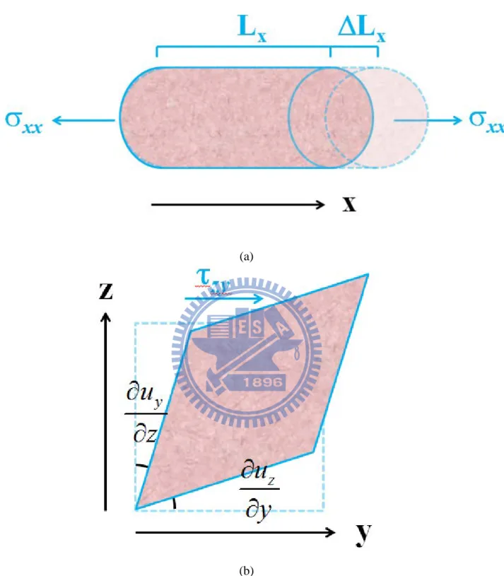
Fig. 3.1 Schematic of an arbitrary force F acting on a surface, along with the resolved components: Fx and Fy, which are the source of shear stress, and Fz, which is
the source of normal stress………..41 Fig. 3.2 (a) Schematic of deformation of a body applied to normal stress along x-axis;
XII
x-axis………42 Fig. 3.3 The schematic energy-band diagram of the n+ polysilicon/SiO2/p-Si MOS
system under uniaxial compressive stress along <110> on (001) substrate. The black-solid lines represent the conduction and valence band edge without the stress. The blue- and green-solid lines represent the stress induced conduction band splits. The electron direct tunneling current (EDT) from the subband levels is also shown………...43 Fig. 3.4 The schematic silicon conduction-band structure in terms of six
constant-energy surfaces in the Brillouin zone. The electron effective masses in the presence of a uniaxial compressive stress are also labeled………44 Fig. 3.5 Comparisons of the measured (symbols) gate current change due to the
external uniaxially compressive stress [3.6] with the calculated (lines) ones obtained using the nominal values in Table 3.2 for the electron effective masses. The process parameters used are Nsub = 1017 cm-3, tox = 1.3 nm, and
Nploy = 1020 cm-3. Poor fitting is encountered if the piezo-effective-mass
coefficients are not included……….45 Fig. 3.6 Comparison of the data (symbols) [3.6] with the calculated results (lines) for (a) πm,z∆4 = 0.03 m0/GPa (dash lines); and πm,z∆4 = 0.03 m0/GPa and πm,d∆2 =
-0.03 m0/GPa (solid lines); (b) πm,z∆4 = 0.05 m0/GPa (dash lines); and πm,d∆4 =
0.05 m0/GPa and πm,d∆2 = -0.02 m0/GPa (solid lines); and (c) πm,z∆4 = 0.07
m0/GPa (dash lines); and πm,d∆4 = 0.07 m0/GPa and πm,d∆2 = -0.017 m0/GPa
(solid lines). πm,z∆2 and πm,d∆4 both are zero………46
Fig. 3.7 The calculated gate current change ratio and its decoupling into different components: the impact frequency f∆2/4, the transmission probability Pt,∆2/4,
and the electron density N∆2/4. One can see that the repopulation of the valley is the main factor responsible for the gate current change…………48
XIII
Fig. 3.8 Comparisons of the measured (symbols) [3.7] and calculated (lines) gate current change due to the process induced compressive stress in the <110> direction. Except the piezo-effective-mass coefficients used correspond to Fig. 3.6(c): πm,z∆4 = 0.07 m0/GPa, πm,d∆2 = -0.017 m0/GPa, πm,z∆2 = 0, and
πm,d∆4 = 0………..49
Fig. 3.9 Comparisons of the measured (symbols) [3.7] and calculated (lines) gate current change due to the process induced compressive stress in the <110> direction. Except the piezo-effective-mass coefficients used correspond to Fig. 3.6(c): πm,z∆4 = 0.07 m0/GPa, πm,d∆2 = -0.017 m0/GPa, πm,z∆2 = 0, and
πm,d∆4 = 0. πtox = 0.012 nm/GPa is used here………50
Chapter 4
Fig. 4.1 The energy band diagram in a poly gate/SiO2/p-substrate system…………..68
Fig. 4.2 The flow chart of the calculation process in NEP………...69 Fig. 4.3 Subband levels calculated by the NEP (solid dots) and by Schred (lines) for two cases as Fig. 2.3………...70 Fig. 4.4 Comparison between Eq. (4.13a) and (4.13b) which are calculated by NEP (Solid line). The dashed line is the line with a slope of 1 and through the origin………71 Fig. 4.5 All the phonon scattering mechanisms. Intravalley scattering involves
acoustic phonon; and long range intervalley scattering and short range intervalley scattering involve g-type optical phonon and f-type one, respectively………...72 Fig. 4.6 Comparison of the mobility calculated by this work (lines) and the
XIV
impurity scattering, phonon scattering, and surface roughness scattering………..73 Fig. 4.7 The total mobility (lines) obtained by Matthiessen’s rule, and the simulated total mobility, phonon and surface roughness limited mobilities (lines with symbols) versus Eeff for (a) Nsub = 5×1017 cm-3,and (b) Nsub = 1017 cm-3 at
300K. The arrow indicates the critical Eeff where phonon and surface
roughness limited mobilities have the same value. The inset shows corresponding population of two lowest subbands……….74
Chapter 5
Fig. 5.1 Schematic diagram of one ∆2 valley and two ∆4 valleys in kx-ky plane. The
channel length direction is along <110> uniaxial tensile stress direction on (001) substrate. Dashed line around the ∆2 valley in terms of the
longitudinal and transverse piezo-effective-mass coefficients, as well as the ∆4 out-of-plane piezo-effective-mass coefficient, shows the effect of stress.
The two insets are added: one for the listed values of the piezo-effective-mass coefficients used for simulation in Figs. 5.3 and 5.4; and the other for the effect of ∆4 out-of-plane piezo-effective-mass
coefficient……….82 Fig 5.2 Comparison of simulated mobility enhancement (cross symbols) due to <110> 170MPa with all πm=0 [5.2] and those (lines) obtained in this work under
different conditions (substrate doping concentration Nsub of 1015 and 1017 cm-3;
and Nsub of 1017 cm-3 without surface roughness scattering). The simulated
mobility enhancement values (lines) are comparable of each other, indicating that phonon scattering dominates. Other simulation lines are produced to
XV
highlight the impact of the ∆4 out-of-plane piezo-effective-mass coefficient
alone. Experimental data (squares and circles) [5.2] are together plotted for comparison………...83 Fig. 5.3 Comparison of mobility enhancement data (symbols) [5.2] under <110> and
<-110> 170 MPa tensile stress with the simulated ones (lines) for four different conditions in Fig. 1, plotted versus vertical effective field. The substrate doping concentration of 1017 cm-3 is used in this work. The inset shows the comparison of simulated mobility enhancement versus tensile strain with the published simulation values [5.2]………...84 Fig. 5.4 Comparison of gate current change data (symbols) [5.12], [5.14] at Vg = 1 V
with those (lines) simulated under four different conditions in Fig. 5.1, plotted versus <110> tensile stress magnitude. The gate oxide thickness and substrate doping concentration used in simulation are 1.3 nm and 5×10¹⁷
cm-3, as in [5.12]………85
Chapter 6
Fig. 6.1 The schematic of the triple-gate FinFET with the different crystal orientations……….98 Fig. 6.2 Subband levels calculated by the Schred [6.4] (lines) and by NEP (dots) for two cases: (a) (110) nMOSFET; and (b) (111) nMOSFET. Both of them are with the same process parameters………..99 Fig. 6.3 Repeating the same work as in Fig. 4.5 on (110) and (111) nMOSFET. The
parameters we used are listed in Table 4.1 except ∆ = 0.2nm is used in (111) case………...100 Fig. 6.4 The NEP simulated mobility ratio (dots) due to stress. Three orientations
XVI
nMOSFET are involved: (a) (001)/<110>, (b) (110)/<1-10>, and (c) (111)/<1-10>. Longitudinal, transverse, vertical, and biaxial stresses are considered for each orientation. All are simulated with Nsub = 1017cm-3 and
Eeff = 1MV/cm. In (a) and (b), the simulated work by [6.7] is together
shown for comparison………101 Fig. 6.5 The energy band diagram in a double-gate nMOSFET………103 Fig. 6.6 (a) Subband energy versus gate voltage and (b) the respective wave-function
of double-gate MOSFET with Nsub=1x1016cm-3, tsi=30nm, and
tox=5nm……….104
Fig. 6.7 (a) Subband energy versus gate voltage and (b) the respective wave-function of double-gate MOSFET with Nsub=1x1016cm-3, tsi=1.5nm, and
tox=5nm……….105
Fig. 6.8 The comparison of potentials and electron density distributions structure at
5
5 10 V/cm
eff
E = × in (a) tSi=30nm and (b) tSi=5nm with Shoji's data
[6.11]………106 Fig. 6.9 Subband energies as function of Si thickness tSi at
5
1 10 /
eff
E = × V cm and the comparison with Shoji's data [6.11]………...107 Fig. 6.10 Subband occupancy versus inversion charge for different Si strain. Symbols: Brain's results [6.12]; Lines: this work. The effective mass m* =0.5m0is used in SiO2 regions, and biaxial tensile strain 1%=1.8GPa [6.6]……….108
Fig. 6.11 The 0.2nm perturbation of surface roughness assumed in 5nm-film double-gate structure. The Hamiltonians of the perturbation is calculated using (6.3) and (6.4). significant difference between these two models can be observed………...109
XVII
Fig. 6.12 The DG-NEP simulated mobility ratio (dots) due to stress. Three orientations nMOSFET are involved: (a) (001)/<110>, (b) (110)/<1-10>, and (c) (111)/<1-10>. Longitudinal, transverse, vertical, and biaxial stresses are considered for each orientation. All are simulated in Nsub
=1017cm-3 and Eeff =1MV/cm………...110
Fig. 6.13 Comparison of calculated electric field (solid line) between Eq. (4.13b) and (6.5) using DG-NEP. The dashed line is the line with a slope of 1 and through the origin………...112
1
Chapter 1
Introduction
1.1 Motivation
During the period of increasing device density in silicon integrated circuits, many problems are encountered and needed to be solved, such as the degradation of mobility, increasing of the leakage current, enhancement of the DIBL effect, and the existence of process-induced mechanical stress. Many researchers tried replacement materials of silicon while other researchers pointed out that the applied stress as well as non-planar structures can be utilized to improve the electrical properties.
The planar MOSFET with its single gate is the general structure of device. The control ability of its single gate is designed with the scaling down. Other novel structures, such as double-gate MOSFET, FinFET, and nanowire, could help increase the control of the gate and decrease the parasitic capacitance. Those could improve the annoying short channel effect. As the particle is confined strongly, some physical effects emerge. The particle penetration into the gate barrier is getting easier. Thus, we should take more care about the resulting tunneling current across the gate dielectrics. Furthermore, the particle is easily confined by space barrier instead of interior electric field, the case of “volume inversion”.
Strain has one main effect in term of the energy band shift and warp is (especially for hole), which in turn affects the electrical performance such as mobility [1.1]-[1.3], threshold voltage [1.4], and gate direct tunneling current [1.5]-[1.7]. These are due to the strain-induced band distortion that changes the energy level, population,
2
effective mass and scattering time in each valley. To take the merits of the strain effect, many of the processes used in silicon IC fabrication individually and cooperatively contribute to the development of favorable stress as in the silicon active region.
Some researches also mentioned that the process induced stress has influence on the gate oxide, such as integrity and growth rate. This can induce more leakage current across the gate. In the IC industry nowadays, tunneling is a terrible phenomenon such as standby power consumption, leakage current in C-V measurement, etc. [1.8]-[1.9]. Thus, a computationally efficient and reasonable physical model for characterizing the gate direct tunneling current of strained silicon device is essential. Besides, the more efficient and faster device is needed in each generation, especially for high mobility. Applied stress is one of the methods that can boost mobility. Thus, physical model that can estimate mobility under stress is needed.
From the gate direct tunneling current and mobility of the strained nMOSFETs, two important physical phenomena are brought out and provided. One is the growth rate of silicon dioxide effects by process stress; another is that effective mass varies with stress as that can be quantified by piezo-effective-mass coefficients. By fitting to the experimental data, both of them can be extracted.
To understand the physics of these situations, we have built a sophisticated calculation tool to simulate the electrical properties of nMOSFET. Although the existing programs are popular in the field, the code is not available and difficult to modify. On the other hand, our simulator built on MATLAB is a good tool to provide enough information for our research. In this thesis, we show the applicability and validity of our simulator in deal with the gate direct tunneling current and mobility.
3
1.2 Dissertation Organization
In Chapter 2, a simulator based on a triangular potential approximation, named “TRP”, is introduced. However, a huge error is accompanied with this method. New algorithm with a corrected coefficient “ηi” embedded in original TRP, is proposed to
eliminate this error.
In Chapter 3, the strain and stress are introduced. The band shift caused by strain is considered in TRP. From the fitting of experimental gate direct tunneling current data by TRP, the importance and values of the piezo-effective-mass coefficients are brought out. We also compare those extracted piezo-effective-mass coefficients with those published in the literature.
In Chapter 4, a powerful simulator of fully Schrődinger and Poisson self-consistent solver for n-channel MOSFETs, named “NEP”, is presented. With the outputs such as subband energy level, inversion charge density, wave-function, etc., we can estimate mobility with key scattering mechanisms included. Gate direct tunneling can be gotten form NEP. Once again, stress effect is considered inside NEP. In Chapter 5, from the fitting of experimental gate direct tunneling current and mobility at the same time, we provide another evidence for the existence and importance of the piezo-effective-mass coefficients.
In Chapter 6, each of (001), (110), and (111) nMOSFETs are discussed under longitudinal, transverse, vertical, and biaxial stress conditions. The double-gate version of the simulator is introduced.
4
5
References
[1.1] J. Welser, J. L. Hoyt, and J. F. Gibbons, “NMOS and PMOS transistors fabricated in strained silicon/relaxed silicon-germanium structures,” in IEDM
Tech. Dig., 1992, pp. 1000-1002.
[1.2] C. H. Ge, C. C. Lin, C. H. Ko, C.C. Huang, Y. C. Huang, B. W. Chan, B. C. Perng, C. C. Sheu, P. Y. Tsai, L. G. Yao, C. L. Wu, T. L. Lee, C. J. Chen, C. T. Wnag, S. C. Lin, Y. C. Yeo, and C. Hu, “Process-strained Si (PSS) CMOS technology featuring 3D strain engineering,” in IEDM Tech. Dig., 2003, pp. 73-76.
[1.3] S. E. Thompson, M. Armstrong, C. Auth, M. Alavi, M. Buehler, R. Chau, S. Cea, T. Ghani, G. Glass, T. Hoffman, C. H. Jan, C. Kenyon, J. Klaus, K. Kuhn, Z. Ma, B. Mcintyre, K. Mistry, A. Murthy, B. Obradovic, R. Nagisetty, P. Nguyen, S. Sivakumar, R. Shaheed, L. Shifren, B. Tufts, S. Tyagi, M. Bohr, and Y. El-Mansy, “A 90-nm logic technology featuring strained-silicon,” IEEE Trans. Electron
Devices, vol. 51, no. 11, pp. 1790-1797, Nov. 2004.
[1.4] J. S. Lim, S. E. Thompson, and J. G. Fossum, “Comparison of threshold-voltage shifts for uniaxial and biaxial tensile-stressed n-MOSFETs,” IEEE Electron
Device Lett., vol. 25, no. 11, pp. 731-733, Nov. 2004.
[1.5] A. Hamada, T. Furusawa, N. Saito, and E. Takeda, “A new aspect of mechanical stress effects in scaled MOS devices,” IEEE Trans. Electron Devices, vol. 38, no. 4, pp. 895-900, Apr. 1991.
[1.6] W. Zhao, A. Seabaugh, V. Adams, D. Jovanovic, and B. Winstead, “Opposing dependence of the electron and hole gate currents in SOI MOSFETs under uniaxial strain,” IEEE Electron Device Lett., vol. 26, no. 6, pp. 410-412, Jun. 2005.
6
[1.7] X. Yang, J. Lim, G. Sun, K. Wu, T. Nishida, and S. E. Thompson, “Strain-induced changes in the gate tunneling currents in p-channel metal-oxide-semiconductor field-effect transistors,” Appl. Phys. Lett., vol. 88, no. 5, pp. 052108-1-052108-3, Jan. 2006
[1.8] S. H. Lo, D. A. Buchanan, Y. Taur, and W. Wang, “Quantum-mechanical modeling of electron tunneling current from the inversion layer of ultra-thin-oxide nMOSFETs,” IEEE Electron Device Lett., vol. 18, no. 5, pp. 209-211, May 1997.
[1.9] K. N. Yang, H. T. Huang, M. C. Chang, C. M. Chu, Y. S. Chen, M. J. Chen, Y. M. Lin M. C. Yu, M. Jang, C. H. Yu, and M. S. Liang, “A physical model for hole direct tunneling current in p+ poly-gate pMOSFETs with ultrathin gate oxides,”
IEEE Trans. Electron Devices, vol. 47, no. 11, pp. 2161-2166, Nov. 2000.
[1.10] Y. T. Hou, M. F. Li, Y. Jin, and W. H. Lai, “Direct tunneling hole currents through ultrathin gate oxides in metal-oxide-semiconductor devices,” J. Appl.
7
Chapter 2
Triangular Potential based Simulator
2.1 Introduction
A simulator based on a triangular potential approximation, named TRP, is presented in this chapter. Some electrical properties of nMOSFET are calculated by
TRP. However, when comparing with the self-consistent Schrődinger and Poisson’s
equations solver, Schred [2.1], unacceptable error appears. Thus, a new algorithm is proposed and incorporated to correct the error.
2.2 Triangular Potential Approximation
2.2.1 Physical Model
The description below is dedicated to the case of (100) nMOSFET. The energy band diagram of poly-gate MOSFET is given in Fig. 2.1, where Vs, Vox, and Vpoly are
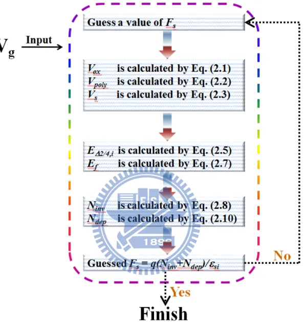
the potential drop in the Si substrate, silicon dioxide, and poly gate region, respectively, Ef is the electron Fermi level, and Fs is the surface electric field. This
band diagram is characterized by Fs. As we give a value of Fs, the Vox is calculated via
continuous electric displacement (i.e., no charge) at the interface:
si ox s ox ox
V
F
ε
t
ε
=
(2.1)8
in the poly depletion region can be calculated:
2
2
si s poly polyF
V
qN
ε
=
(2.2)where q is the elementary charge of an electron and Npoly is the doping concentration
of poly gate. Vs can be expressed as a function of the gate bias Vg:
V
s=
V
g−
V
ox−
V
poly+
V
fb (2.3) where the flat band voltage Vfb is calculated as:
ln(
2)
poly sub fb B iN
N
V
k T
n
= −
(2.4)where Nsub is the doping concentration of substrate, ni is the intrinsic carrier density in
substrate, kB is the Boltzmann’s constant, and T is the absolute temperature. The
solving of the Schrődinger equation in the quantum-confined direction normal to the
SiO2/Si surface yields the ∆2 subband level i in the absence of the stress [2.2]:
3 2 3 1 2 , 2 , 2
))
4
1
(
2
3
(
)
2
(
−
=
∆ ∆qF
i
m
E
s z iπ
(2.5)The average depth of the 2DEG is:
2,i
2
2,i/ 3
sZ
∆=
E
∆qF
(2.6)where mz,∆2 is the ∆2 quantization effective mass, is the Planck’s constant divided
by 2π. Eq. (2.5) can apply to 4-fold case by replacing ∆2 with ∆4. From Fig. 2.1, the
9 ln( sub) f s g B v N E V E k T N = − − (2.7)
where Eg is the energy gap of silicon, Nv is the effective density of states in valence
band. With Eq. (2.5) and (2.7), we can get the charge density for each subband [2.3]:
2/4, 2/4( d, 2/42 B ) ln(1 exp( f 2/4,i)) i B E E m k T N g k T π ∆ ∆ ∆ ∆ − = + (2.8) where g∆2/4 is the ∆2 /∆4 valley degeneracy; and md,∆2/4 is the 2-D density-of-states
(DOS) effective mass of the ∆2 /∆4 valley.
The surface drop due to bulk depletion Vdep and 2D depletion charge density Ndep are
[2.2]: inv qm B dep s si
qN Z
k T
V
V
q
ε
=
−
−
(2.9) 2 si dep sub dep V N N qε
= (2.10)where Ninv is 2D inversion charge density which is equal to the summation of N∆2/4,i,
and Zqm is the average penetration of the inversion-layer charge from the surface. As
we give a gate voltage Vg as input, initial Fs is guessed until it is consistently equal to
( inv dep) / si
q N +N
ε
according to Gauss law. The flow chart is presented in Fig. 2.2. On the other hand, if the device is manufactured by metal gate, the potential drop of metal gate is equal to zero and the flat band voltage relates to work function.10
2.2.2 Outcome of TRP
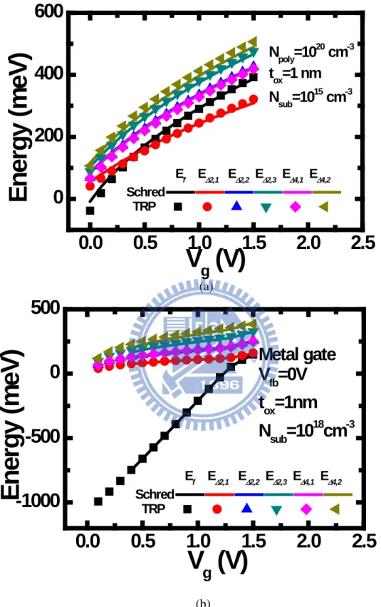
In Fig. 2.3, the resulting conduction potential profile is shown, along with five lowest subband levels for (100) nMOSFETs in terms of three of ∆2 subband and two
of ∆4 subbnad. We show both cases of poly silicon and metal gate. To examine the
validity of the triangular potential approximation, a self-consistent Poisson-Schrödinger equations solver, Schred [2.1], was used and the resulting subband levels are shown in Fig. 2.3. In the figure, the drawback of the conventional triangular potential approximation is clear, especially in the higher energy levels where the corresponding electric field deviates from the surface field Fs, as shown in
Fig. 2.1.
2.3 Correction Coefficient Generator
To address this issue, different methods have been proposed previously: (i) the variation approach dedicated to the correction of the lowest subband [2.2], [2.4]; and (ii) the effective field Feff to replace Fs in Eq. (2.5) [2.5]-[2.10]:
(
inv dep)
eff siq
N
N
F
η
ε
+
=
(2.11)The correction coefficient η in Eq. (2.11) is constant with a spanned range from 0.5 to 1.0: η = 0.75 for ∆2 and 1.0 for ∆4 [2.5], [2.6]; η = 0.5 for all subbands [2.7]; and
η = 0.75 for all subbands [2.8]-[2.10]. However, the previous improvements that led to Eq. (2.11) are not enough from the aspect of the direct tunneling: each of the subbands involved in the tunneling should have its own correction coefficient such as
11
to ensure the proper direct tunneling calculation. Obviously, due to different electric fields encountered from level to level as revealed in Fig. 2.1, different correction coefficient values should correspond to different subbands. To take this into account, we suggest the individual correction coefficient η∆2,i for the ∆2 level i and the
corresponding effective electric field can be written as:
2, 2, ( i inv dep) i si q N N F
η
ε
∆ ∆ + = (2.12)The same procedure can apply to ∆4 case: F∆4,i corresponds to η∆4,i. Again, to quantify
the correction coefficient values, the solver Schred [2.1] was conducted in a MOS system on (001) silicon surface. A wide range of the key process parameters was included: the substrate doping concentration Nsub= 1015, 1016, 1017, and 1018 cm-3; the
gate oxide thickness tox = 1, 3, and 6 nm; and the different gate stacks in terms of a
polysilicon and a metal electrode. By matching the subband levels produced by
Schred with those from Eq. (2.5) (with Fs replaced by F∆2,i for 2-fold valley and F∆4,i
for 4-fold valley), the values of the η∆2,i and η∆4,i result. A scatter plot between the correction coefficient values and the corresponding subband levels is given in Fig. 2.4, which is made with the surface field Fs as a parameter. Strikingly, the figure points to
two relevant relationships. First, under fixed Fs, all data points fall on or around a
straight line, indicating that the correction coefficient depends linearly on the subband level. Second, the straight line appears to shift with Fs. This specific behavior can be
modeled by the intercept, designated as ηo, of the extrapolated line at zero subband
level. In the inset of the figure, ηo is plotted against Fs, clearly showing another linear
relationship, regardless of the Nsub, tox, or gate stack material. This is expected from
12
relationships therefore leads to a subband-level correction-coefficient generating expression suitable for both ∆2 and ∆4 [2.11]:
2 / 4,i
0.003
E
2 / 4,i(1.01 0.308
F
s)
η
∆= −
∆+
+
(2.13)The units of E∆2/4i and Fs in Eq. (2.13) are meV and MV/cm, respectively. Eq. (2.13)
can provide a transparent understanding of the effect of the subband level and surface field on the calculated correction coefficient. Interestingly, Eq. (2.13) is also self-consistent: for those of the subband levels close to the reference point (that is, the classical conduction band edge at the surface), the correction coefficients lie in close proximity of unity and hence the effective electric field approaches the surface one. To testify to the validity of Eq. (2.13) in the subband level calculation, the results are compared with those from Schred [2.1], as given in Fig. 2.5 for two different gate stacks. Excellent agreements are evident, obtained without adjusting any parameters. Note that the expression Eq. (2.13) is valid only for (001) substrate. Further study is needed concerning the underlying physical origins as well as its applicability to other substrate orientations. We think that the two linear relationships in Fig. 2.4 may be helpful in this direction.
13
References
[2.1] Schred. [Online]. Available: http://nanohub.org/resources/schred.
[2.2] F. Stern, “Self-consistent results for n-type Si inversion layers,” Phys. Rev. B, vol. 5, no.12, pp.4891-4899, Jun. 1972.
[2.3] F. Stern and W. E. Howard, “Properties of semiconductor surface inversion layers in the electric quantum limit,” Phys. Rev., vol. 163, no. 3, pp. 816–835, Oct. 1967.
[2.4] N. Yang, W. K. Henson, J. R. Hauser, and J. J. Wortman, “Modeling study of ultrathin gate oxides using direct tunneling current and capacitance-voltage measurements in MOS devices,” IEEE Trans. Electron Devices, vol. 46, no. 7, pp. 1464–1471, Jul. 1999.
[2.5] J. S. Lim, X. Yang, T. Nishida, and S. E. Thompson, “Measurement of conduction band deformation potential constants using gate direct tunneling current in n-type metal oxide semiconductor field effect transistors under mechanical stress,” Appl. Phys. Lett., vol. 89, no. 7, pp. 073509-1-073509-3, Aug. 2006.
[2.6] C. Y. Hsieh and M. J. Chen, “Measurement of channel stress using gate direct tunneling current in uniaxially stressed nMOSFETs,” IEEE Electron Device
Lett., vol. 28, no. 9, pp. 818-820, Sept. 2007.
[2.7] C. K. Park, C. Y. Lee, B. J. Moon, Y. H. Byun, and M. Shur, “A unified current-voltage model for long-channel nMOSFET’s,” IEEE Trans. Electron
Devices, vol. 38, no. 2, pp. 399-406, Feb. 1991.
[2.8] Y. Ma, L. Liu, Z. Yu, and Z. Li, “Validity and applicability of triangular potential well approximation in modeling of MOS structure inversion and accumulation layer,” IEEE Trans. Electron Devices, vol. 47, no. 9, pp. 1764-1767, Sept. 2000. [2.9] Y. T. Hou, M. F. Li, Y. Jin, and W. H. Lai, “Direct tunneling hole currents
14
through ultrathin gate oxides in metal-oxide-semiconductor devices,” J. Appl.
Phys., vol. 91, no. 1, pp. 258–264, Jan. 2002.
[2.10] H. Abebe, E. Cumberbatch, H. Morris, and V. Tyree, “Compact models of the quantized sub-band energy levels for MOSFET device application,” in IEEE
UGIM Proceedings, 2008, pp. 58-60.
[2.11] W. H. Lee and M. J. Chen, “Gate direct tunneling current in uniaxially compressive strained nMOSFETs: a sensitive measure of electron piezo effective mass,” IEEE Trans. Electron Devices, vol. 58, no. 1, pp. 39-45, Jan.
15
Fig. 2.1 Silicon energy-band diagram produced by Schred [2.1] (black lines), two calculated subband energy level (pink lines), and the Fermi level (blue line), as well as the red line for the triangular potential approximation under the same surface field.
16
17
0.0
0.5
1.0
1.5
2.0
2.5
0
200
400
600
Ef E∆2,1 E∆2,2 E∆2,3 E∆4,1 E∆4,2 Schred TRPE
n
er
g
y (
m
eV
)
V
g
(V)
N
poly=10
20cm
-3t
ox=1 nm
N
sub=10
15cm
-30.0
0.5
1.0
1.5
2.0
2.5
-1000
-500
0
500
Metal gate
V
fb=0V
t
ox=1nm
N
sub=10
18cm
-3E
n
er
g
y (
m
eV
)
V
g
(V)
Ef E∆2,1 E∆2,2 E∆2,3 E∆4,1 E∆4,2 Schred TRP (a) (b)Fig. 2.3 Subband levels calculated by the triangular potential approximation (solid dots) and by Schred (lines) for two cases: (a) n+ poly silicon doping Npoly = 1020 cm-3,
tox = 1 nm, and Nsub = 1015 cm-3; and (b) metal gate with zero flat-band voltage, tox =
18
Fig. 2.4 The extracted correction coefficient versus the corresponding subband level with the surface field as a parameter. The fitting lines are drawn. The intercept, ηo, of
the extrapolated line at the zero subband level is inserted and plotted versus the surface field. A fitting line is also shown in the inset.
200
400
600
800
0.4
0.6
0.8
0.8
1.2
1.6
2.0
1.2
1.3
1.4
1.5
1.6
η
0 = 1.01 + 0.308 FsFs (MV/cm)
η
0η
∆2
/4
,i
η
∆2,
1
η
∆2
,2
η
∆2,
3
η
∆4,
1
Subband Level (meV)
Fs = 2.0 MV/cm
Fs = 1.5 MV/cm
Fs = 1.0 MV/cm
F
s
= 0.8 MV/cm
19
0.0
0.5
1.0
1.5
2.0
2.5
0
200
400
600
Ef E∆2,1 E∆2,2 E∆2,3 E∆4,1 E∆4,2 Schred TRPE
n
er
g
y (
m
eV
)
V
g
(V)
N
poly=10
20cm
-3t
ox=1 nm
N
sub=10
15cm
-30.0
0.5
1.0
1.5
2.0
2.5
-1000
-500
0
500
Metal gate
V
fb=0V
t
ox=1nm
N
sub=10
18cm
-3E
n
er
g
y (
m
eV
)
V
g
(V)
Ef E∆2,1 E∆2,2 E∆2,3 E∆4,1 E∆4,2 Schred TRP (a) (b)Fig. 2.5 Repeating the calculation work by the triangular potential approximation based on the new η correction generator.
20
Chapter 3
Strain Altered Electron Gate Direct Tunneling
Current
3.1 Introduction
In this chapter, we discuss about the model of conduction band electron direct tunneling (EDT) current. For the silicon nMOSFETs formed on (001) substrate, the quantum confinement effect [3.1] around the inversion layer makes the bulk conduction band split into two distinctive components: 2-fold (∆2) and 4-fold (∆4)
valleys. The longitudinal effective mass (ml) and transverse effective mass (mt)
associated with those subband valleys essentially remain intact [3.1]. The energetic difference between ∆2 and ∆4 levels can be further changed via the applied mechanical
stress as in the state-of-the-art strain engineering. The stress induced subband shift has been thoroughly studied theoretically [3.2] in terms of the deformation potential constants [3.3]-[3.5]. Thus, the change ratio of EDT current under strain can be estimated.
Comparing with the experimental data of EDT current [3.6], [3.7], one important physical phenomenon can be brought out: the effective mass of electron varies with applied stress. Recently, the sophisticated band-structure calculation [3.8]-[3.10] on (001) silicon surface has pointed out that only with the strain dependence of ml and mt
taken into account can the strain induced mobility change be elucidated. The significance of the strain dependent electron effective masses in (110) case has also been mentioned [3.11]. Thus, in addition to the deformation potential counterparts, the
21
strain dependence of ml and mt or equivalently the electron piezo-effective-mass
coefficient, πm, should not be absent in the strain altered conduction-band structure.
The mobility measurement method has been constructed to experimentally determine the πm of electrons [3.12]. On the other hand, the effect of the mechanical
stress on the electron gate direct tunneling current has been experimentally observed [3.6], [3.7], [3.13]-[3.17]. In the citations [3.6], [3.7], [3.13]-[3.17], however, the impact of the πm on the strained electron gate direct tunneling current has not been
noticed. According to the quantum confinement picture [3.1], a change in the electron quantization effective mass due to the stress will produce a change in the subband level and therefore change the transmission probability dramatically. Thus, through the inverse modeling technique, the electron gate direct tunneling current in strained device may serve as a sensitive detector of πm. However, few studies on this subject
were done to date..
3.2 Strain-Altered Band Structures
In this section, we make a connection between the strain and the stress. Notice that the temperature-induced strain does not be considered here. Stress is the average force over the area on which the force acts. Thus, the intensity of stress is expressed as function of applied force per area. The force applied on an area can be separated into two directions: out-of-plane direction (normal force) and in-plane direction (shear force). The stress caused by normal/shear force is called normal/shear stress.
For a force F applied on an infinitesimal area A which is normal to the z direction, as show as in Fig. 3.1, the projected quantity of the force along x, y, and z are Fx, Fy,
22
and Fz, respectively. Then the normal stress σzz and shear stress τzx and τzy are
defined: 0
lim
z zz AF
A
σ
→=
(3.1a) 0lim
x zx AF
A
τ
→=
(3.1b) 0lim
y zy AF
A
τ
→=
(3.1c)The notation σii refers to the normal stress acting on the plane perpendicular to
i-direction, and τij refers to the shear stress component along j-direction acting on the
plane perpendicular to i-direction.
Furthermore, we consider the case of an infinitesimal cube whose six surfaces face to ±x, ±y, and ±z. There should be 18 stress components by Eq. (3.1). However, two conditions are observed: (1) Fx and F-x are reaction force of each other;
(2) τxy= τyx, τyz= τzy, and τzx= τxz can be derived because of the total applied force
and torque on the cube are zero. Thus, stress tensor is simplified to the only 6 terms [3.18]: xx yy zz yz zx xy
σ
σ
σ
σ
τ
τ
τ
=
(3.2)23
It is notable that the tensile stress is shown as positive value. On the other hand, the compressive stress is the negative value. With external stress, a deformable body changes its size and shape. In Fig. 3.2(a), a normal tensile force along x-direction σxx
is applied on deformable body and the length along x-direction is increased. The normal strain is defined:
𝜀
𝑥𝑥=
∆𝐿𝐿𝑥𝑥 (3.3)Again, positive ε means the length elongates, a situation called tensile strain. Negative ε means that the length is contracted, the case compressive strain.
In Fig. 3.2(b), a shear stress τzy is applied on a planar body that causes the change
of its shape. The angle varies from π/2 to q. Besides, the lengths of four side lines are unchanged. The shear strain γzy is defined as the change in the angle between two
neighbor sidelines of the square on y-z surface [3.18]:
2
z y zy zyu
u
y
z
γ
=
ε
=
∂
+
∂
∂
∂
(3.4)where uz and uy mean the displacements along z- and y-direction respectively. γzy
presents the shear strain, and εzy is the average shear strain equal to the half of γzy
[3.18]-[3.20].
Similar to stress tensor, the strain tensor is also composed of six independent components:
24 xx yy zz yz zx xy
ε
ε
ε
ε
γ
γ
γ
=
(3.5)When a stress is applied to a homogeneous and isotropic material, the normal strain has a linear relationship with normal stress, which is the well-known Hooke’s Law [3.18]-[3.20]:
E
σ
=
ε
(3.6) where the constant of proportionality E is the Young’s modulus. Furthermore, while the normal stress is applied on elastic material, the strain transversal to stress usually accompanies. The relationship between normal strain and transverse strain is [3.18]-[3.20]:
ε
tran= −
v
ε
long (3.7) where the constant of proportionality v is the Poisson’s ratio. Finally, the Hooke’s law still holds for shear strain [3.18]-[3.20]:
τ
=
G
γ
(3.8) where the constant of proportionality G is the shear modulus.With Eq. (3.6)-(3.8), the relation between strain and stress is: xx
1
[
xxv
(
yy zz)]
E
25
1
[
(
)]
yy yyv
xx zzE
ε
=
σ
−
σ
+
σ
(3.9b)1
[
(
)]
zz zzv
xx yyE
ε
=
σ
−
σ
+
σ
(3.9c)1
xy xyG
γ
=
τ
(3.9d)1
yz yzG
γ
=
τ
(3.9e)1
xz xzG
γ
=
τ
(3.9f)For simplicity, we usually transfer the strain and stress relationships to the matrix form. With Eq. (3.2), (3.5), and (3.9), the elastic relationship between strain and stress is established [3.18]-[3.22]: 11 12 12 12 11 12 12 12 11 44 44 44
0
0
0
0
0
0
0
0
0
2
0
0
0
0
0
2
0
0
0
0
0
2
0
0
0
0
0
xx xx yy yy zz zz yz yz zx zx xy xyS
S
S
S
S
S
S
S
S
S
S
S
ε
σ
ε
σ
ε
σ
ε
τ
ε
τ
ε
τ
=
(3.10)where S is the compliance coefficient. S11 is equal to 1/E, S12 is equal to -v/E, and S44
is equal to 1/G. For the silicon case, the experimental values are: S11 = 7.68x10⁻¹²
m2/N, S12 = -2.14x10⁻¹² m2/N, and S44 = 12.6x10⁻¹² m2/N [3.23]-[3.26].
In deformation potential theory, the total Hamiltonian for each energy valleys of silicon conduction band is [3.27]:
2 2 2 2 0
(
)
(
)
(
(
)
)
2
2
l t c d ij u l l lk
k
k
H
E
Tr
m
m
ε
ε
−
=
+
+
+ Ξ
+ Ξ
(3.11)26
where kl and kt are the wavevectors parallel and perpendicular to the axis where the
valleys are located, respectively, Ξd and Ξu are the hydrostatic and shear deformation
potential constants, respectively, Tr(εij) is the trace of the strain tensor. And Ξd = 1.13
eV and Ξu = 9.16 eV are given in silicon case [3.26], εl is the longitudinal strain
component. Appling Eq. (3.11), the band edge shift for the minima of the six conduction band valleys along the <100> direction is:
∆
E
c x,= Ξ
d(
ε
xx+
ε
yy+
ε
zz)
+ Ξ
uε
xx (3.12a)
∆
E
c y,= Ξ
d(
ε
xx+
ε
yy+
ε
zz)
+ Ξ
uε
yy (3.12b)
∆
E
c z,= Ξ
d(
ε
xx+
ε
yy+
ε
zz)
+ Ξ
uε
zz (3.12c)Actually, the applied stress is not always along [100], it may be in the direction of [110], [111], and [112], etc. Fortunately, the stress is easily transformed between different coordinates [3.18]. The stress tensors in some cases are listed in Table 3.1.
3.3 Gate Direct Tunneling Current Model
Using both quantum mechanical simulator TRP and a modified WKB [3.28]-[3.30] approximation for transmission probability, the model for calculating the gate direct tunneling currents across ultra-thin gate oxides of MOS structures is discuss here.
The correction coefficient generator via Eq. (2.5) and (2.12) were incorporated into existing strain quantum simulator in our previous works [3.29]-[3.31]. The resulting subband level in the presence of the uniaxial channel stress σ in the <110> direction can be written with respect to the non-stress conduction-band edge at the
27 Si/SiO2 interface [3.3]-[3.6]
σ
σ
)( ) 3 ( ) 2 )( 3 ( 11 12 12 11 , 2 ' , 2 E S S S S E∆ i = ∆ i + Ξd +Ξu + + Ξu − (3.13a)σ
σ
)( ) 6 ( ) 2 )( 3 ( 11 12 12 11 , 4 ' , 4 E S S S S E∆ i = ∆ i + Ξd +Ξu + − Ξu − (3.13b)The carrier repopulation under stress can be calculated accordingly:
' , 2 / 4 2 / 4, 2 / 4, 2 / 4( 2 ) ln(1 exp( )) d B F i i B m k T E E N g k T π ∆ ∆ ∆ ∆ − = + (3.14) Finally, the triangular potential based electron gate direct tunneling current density can be computed:
∑
∑
∆ ∆ ∆ + ∆ ∆ ∆ = i i t i i i t i i i e qf N P E qf N P E J 2, 2, ( ' 2, ) 4, 4, ( '4, ) (3.15)where f represents the electron impact frequency on the Si/SiO2 interface and is equal
to (qF∆2/4,i/2)(2mz,∆2/4E∆2/4,i)-1/2; and Pt(E’∆2/4,i) is the electron transmission probability
across the SiO2 film. In Fig. 3.3, the energy band diagram of the MOS system under
study is schematically shown, where the electron direct tunneling process from the subband level is highlighted. Throughout the work, only five lowest subbands (3 of ∆2
and 2 of ∆4) will be adopted to calculate the gate current.
Here, the electron effective mass in the oxide for the parabolic type dispersion relationship was used with mox = 0.50 mo, which is equivalent to mox = 0.61 mo for the
tunneling electrons in the oxide using the Franz type dispersion relationship [3.32]. The SiO2/Si interface barrier height in the absence of stress is 3.15 eV. Given the
situations that the deformation potential constants are known and the channel stress can be determined by other means, there are four variables in using (3.15) to quantify
28
the gate direct tunneling current: (i) the 2-fold quantization effective mass mz,∆2; (ii)
the 2-fold 2-D DOS effective mass md,∆2; (iii) the 4-fold quantization effective mass
mz,∆4; and (iv) the 4-fold 2-D DOS effective mass md,∆4. The DOS effective mass can
relate to the mentioned ml and mt of the valley: md,∆2 = (mt,∆2|| mt,∆2⊥)1/2 and md,∆4 =
(ml,∆4 mt,∆4)1/2, where mt,∆2|| and mt,∆2⊥ are the in-plane transverse effective mass of ∆2
in the direction parallel and perpendicular to the stress direction, respectively; and
ml,∆4 and mt,∆4 are the in-plane longitudinal and transverse effective mass of ∆4,
respectively. All the effective masses involved in this work are depicted in Fig. 3.4 in terms of the conduction-band structure in the Brillouin zone. The corresponding nominal values (i.e., in the absence of the stress) are listed in Table 3.2.
3.4 Data Fitting
In Fig. 3.5, the gate current density calculated by TRP and that from experiment [3.6] for different gate voltages are shown. Unlike the results from original TRP, our modified TRP provides deviating with the experimental one. Even if we tried other different nominal values for the effective masses in silicon, the deformation potential constants, the effective mass in the oxide, the doping concentration, the gate oxide thickness, etc., a poor fitting like that in Fig. 3.5 still remained.
Obviously, for a general effective mass m, the piezo-effective-mass coefficient πm must be added:
σ
π
σ
z mz zm
m
(
)
=
(
0
)
+
, (3.16a)σ
π
σ
d md dm
m
(
)
=
(
0
)
+
, (3.16b)29
Here, a small stress is imposed to make possible the linear approximation that ensures the validity of (3.16). To assess the underlying πm (πm,z∆2, πm,d∆2, πm,z∆4, and πm,d∆4), the
sensitivity analysis was performed during the data fitting. First of all, one of these four πm factors were alternately selected in applying (3.16), with the remaining three
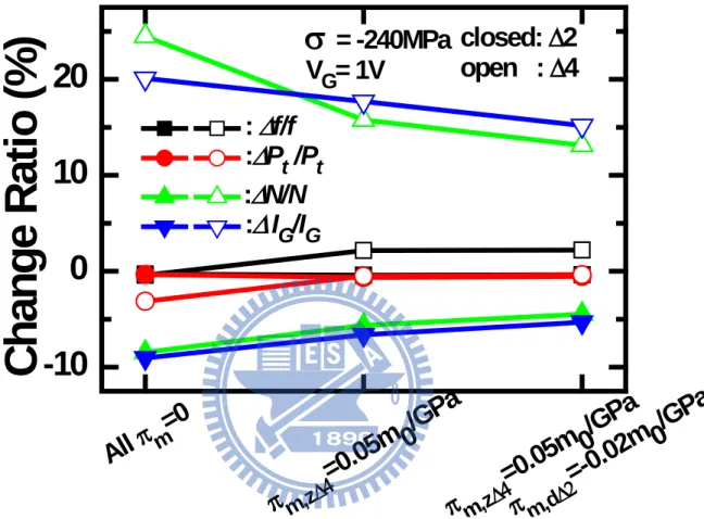
kept at zero. Strikingly, we found that the πm,z∆4 is the primary factor because it can
have a strongest effect on the calculated gate current change, as illustrated in Fig. 3.6 for πm,z∆4 of 0.03, 0.05, and 0.07 mo/GPa. It can be seen from the figure that the fitting
can be somewhat improved by simply increasing πm,z∆4. Next, we also found that the
πm,d∆2 can serve as the secondary factor in refining the calculated gate current change.
This means that both πm,z∆4 and πm,d∆2 are enough in producing the reasonable fitting.
Thus, in the subsequent work, we set πm,z∆2 and πm,d∆4 to zero. A set of the πm,z∆4 and
πm,d∆2 values was hence extracted from the best fitting, as displayed in Fig. 3.6: (i)
πm,z∆4 = 0.03 mo/GPa and πm,d∆2= -0.03 mo/GPa; (ii) πm,z∆4 = 0.05 mo/GPa and πm,d∆2 =
-0.02 mo/GPa; and (iii) πm,z∆4 = 0.07 mo/GPa and πm,d∆2 = -0.017 mo/GPa. Obviously,
the increasing πm,z∆4 is accompanied with the less negative πm,d∆2. The
piezo-effective-mass coefficient values obtained in the data fitting are listed in Table 3.3.
Here, we give plausible explanations for the assessed πm,z∆4 and πm,d∆2 and
particularly the difference in the polarity between the two. Firstly, a positively increased πm,z∆4 will decrease the ∆4 quantization effective mass (see Eq. (3.16a))
under uniaxial compressive stress, which will in turn increase the ∆4 level. As a result,
due to the repopulation of the valley, more electrons are transferred down to the ∆2
subband and hence the direct tunneling is reduced. Secondly, a less negative πm,d∆2
will increase the effective DOS in ∆2 (see Eq. (3.16b)) under uniaxial compressive

![Table 3.1 The stress tensor for uniaxial stress along [110], [1-10], [001], [111], and [11-2] direction](https://thumb-ap.123doks.com/thumbv2/9libinfo/7702142.144946/57.892.126.753.173.798/table-stress-tensor-uniaxial-stress-direction.webp)
![Table 3.2 The nominal values of the electron effective masses in the absence of the mechanical stress in [3.8]-[3.10], [3.12]](https://thumb-ap.123doks.com/thumbv2/9libinfo/7702142.144946/58.892.123.804.185.738/table-nominal-values-electron-effective-masses-absence-mechanical.webp)
![Table 3.3 Comparison of the electron piezo-effective-mass coefficients from the band-structure calculation and mobility measurement [3.8]-[3.10], [3.12] with those obtained in this work](https://thumb-ap.123doks.com/thumbv2/9libinfo/7702142.144946/59.892.128.810.280.749/comparison-electron-effective-coefficients-structure-calculation-mobility-measurement.webp)