低超取樣率多級和差類比數位轉換器在寬頻通訊系統上之研究
133
0
0
全文
(2) The Dissertation Committee for Teng-Hung Chang certifies that this is the approved version of the following dissertation:. Study on Low Oversampling Ratio Cascaded Σ∆ ADC with 1- or 1.5-bit Feedback DAC for Broadband Telecommunication Applications. Committee:. Lan-Rong Dung, Supervisor Professor Chung-Yu Wu, Committee Chair Professor Jen-Shiun Chiang Professor Wei-Zen Chen Professor Hao-Chiao Hong Professor Jhen-Yu Lin.
(3) Study on Low Oversampling Ratio Cascaded Σ∆ ADC with 1- or 1.5-bit Feedback DAC for Broadband Telecommunication Applications. by. Teng-Hung Chang. A Dissertation Submitted to Department of Electrical and Control Engineering College of Electrical Engineering and Computer Science National Chiao-Tung University in Partial Fulfillment of the Requirements for the Degree of Doctor of Philosophy in Electrical and Control Engineering September 2007 Hsinchu, Taiwan, Republic of China.
(4) To my parents.
(5) Acknowledgments A long journey has come to an end. I would like to take this opportunity to thank my advisor, Professor Lan-Rong Dung, for his constant support, guidance and encouragement throughout my research without which this thesis would not have been possible. I am also grateful to the members of my dissertation review committee, Professor Chung-Yu Wu, Professor Jen-Shiun Chiang, Professor Wei-Zen Chen, Professor Hao-Chiao Hong, and Dr. Jhen-Yu Lin for their valuable comments and suggestions. I would like to thank Trendchip Technologies Corporation for providing me the internship to design the ADC in an ADSL2+ analog front end chip and for fabrication of the prototype chip of the ADC. Also, I wish to thank Dr. Jwin-Yen Guo and Dr. Hsin-Hsien Li for their valuable discussion during layout and design phases, as well as C.-Y. Hsu and H.-C. Tseng for testing support. I would like to thank members of the System on Chip laboratory both past and present, for their invaluable support, assistance, friendship, and feedback which kept me on track of my research. Also, I am grateful to my classmates, Dr. Hsu-Cheng Hsu and Dr. Chen-Ta Ho for their constant encouragement and sharing in this five-year trip of Ph.D. degree. Finally, I would like thank my parents and rest of my family, for their loving support and encouragement in my pursuit of my academic goals.. Teng-Hung Chang National Chiao-Tung University September 2007. v.
(6) Study on Low Oversampling Ratio Cascaded Σ∆ ADC with 1- or 1.5-bit Feedback DAC for Broadband Telecommunication Applications. Teng-Hung Chang, Ph.D. National Chiao-Tung University, 2007 Supervisor: Lan-Rong Dung. Abstract. The speed and resolution of analog-to-digital converter (ADC) must advance before the signal bandwidth and the modulation depth of digital telecommunications receivers can improve. Hence, the data rate achievable by a communications standard is inevitably linked to the performance of the ADC. Sigma-Delta (Σ∆) ADCs have demonstrated the possibility of achieving very high resolutions (>13 bit) without the need for expensive post-processing techniques, such as laser trimming or calibration. Nevertheless, Σ∆ ADCs have generally a limited signal bandwidth due to their oversampling nature. The basic requirement for a broadband Σ∆ ADC is, therefore, low oversampling ratio and high sampling frequency. Among many existing architectures, continuous-time single-loop architecture, discrete-time single-loop architecture, and discrete-time cascaded architecture are three possible and popular candidates. Considering the advantages and disadvantages of each architecture, this thesis is dedicated to addresses the design of two discrete-time cascaded Σ∆ ADCs with low oversampling ratio (OSR) for broadband telecommunication applications. The first one is a low-power Σ∆ ADC for the extended bandwidth asymmetric digital subscriber line (ADSL2+); it performs 14 bit of resolution at a conversion rate of 4.4 MS/s. The core modulator employs a cascaded 2-1-1 fourth-order loopfilter with three 1.5-bit quanvi.
(7) tizer. A three-stage digital decimation filter following the modulator output is designed to accomplish the complete analog-to-digital conversion. The sampling frequency is 70.4 MHz and the signal bandwidth is 2.2 MHz, which results in an OSR of 16. The circuit is implemented in TSMC 1P5M 0.25-µm CMOS technology and occupies an area of 2.8 mm2 . The measured dynamic range, peak signal-to-noise ratio and peak signal-to-noise-and-distortion ratio are 86 dB, 84 dB, and 77 dB, respectively. The total power consumption is 180 mW from a 2.5-V power supply including decimation filter and reference voltage buffers. The second one is a resonator-based cascaded Σ∆ modulator (RAMSH) for low OSR applications. Based on two resonator topologies, the architecture can be immune to leakage quantization noise caused by circuit nonidealities over a large portion of the input range when OSR is low, and hence the dynamic range can be improved. The key of improving dynamic range is to use a cascade-of-resonator-with-feedforward (HQCRFF) 1-bit modulator in the first stage and makes the modulator from normal modulation mode into a novel oscillation mode. The theoretic analysis of operational condition for oscillation mode is presented and the transient behavior between two modes is also discussed. Finally, the design methodology and simulation results of RMASH are addressed. Without using additional calibration techniques, the dynamic range of the two RMASH architectures, RMASH 2-0 and RMASH 2-2 with the op-amp dc gain of 60 dB, the capacitor mismatch of 0.2%, and the OSR of 8 can be as high as 87 dB and 84 dB respectively.. vii.
(8) Contents Acknowledgments. v. Abstract. vi. List of Tables. xi. List of Figures. xii. Chapter 1 Introduction 1.1. Analog to Digital Conversion. 1 . . . . . . . . . . . . . . . . . . . . . . . . . .. 3. 1.1.1. Quantization . . . . . . . . . . . . . . . . . . . . . . . . . . . . . . .. 4. 1.1.2. Oversampling . . . . . . . . . . . . . . . . . . . . . . . . . . . . . . .. 5. 1.1.3. Performance Metrics . . . . . . . . . . . . . . . . . . . . . . . . . . .. 5. 1.2. Sigma-Delta ADC . . . . . . . . . . . . . . . . . . . . . . . . . . . . . . . . .. 6. 1.3. Motivation and Contribution . . . . . . . . . . . . . . . . . . . . . . . . . . .. 8. 1.4. Thesis Organization . . . . . . . . . . . . . . . . . . . . . . . . . . . . . . . .. 10. Chapter 2 Architecture Survey 2.1. 2.2. 2.3. 2.4. 12. Continuous-Time Σ∆ Modulator . . . . . . . . . . . . . . . . . . . . . . . .. 12. 2.1.1. Excess Loop Delay . . . . . . . . . . . . . . . . . . . . . . . . . . . .. 13. 2.1.2. Clock Jitter . . . . . . . . . . . . . . . . . . . . . . . . . . . . . . . .. 14. Single-Loop Σ∆ Modulator. . . . . . . . . . . . . . . . . . . . . . . . . . . .. 18. 2.2.1. Feedforward Structure . . . . . . . . . . . . . . . . . . . . . . . . . .. 19. 2.2.2. Dynamic Element Matching . . . . . . . . . . . . . . . . . . . . . . .. 24. Cascaded Σ∆ Modulator . . . . . . . . . . . . . . . . . . . . . . . . . . . . .. 26. 2.3.1. Leakage Quantization Noise . . . . . . . . . . . . . . . . . . . . . . .. 27. Summary . . . . . . . . . . . . . . . . . . . . . . . . . . . . . . . . . . . . .. 30. viii.
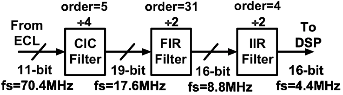
(9) Chapter 3 A Fourth-Order Cascaded Σ∆ ADC for ADSL2+ Application 3.1. 3.2. 3.3. 3.4. 3.5. 32. Architecture . . . . . . . . . . . . . . . . . . . . . . . . . . . . . . . . . . . .. 34. 3.1.1. Design of Analog Modulator . . . . . . . . . . . . . . . . . . . . . . .. 36. 3.1.2. Analysis of 1.5-bit quantization . . . . . . . . . . . . . . . . . . . . .. 40. 3.1.3. Two Pairs of Reference Voltages . . . . . . . . . . . . . . . . . . . . .. 43. 3.1.4. Scaling of Loopfilter Coefficients . . . . . . . . . . . . . . . . . . . . .. 45. 3.1.5. Design of Decimation Filter . . . . . . . . . . . . . . . . . . . . . . .. 47. Circuit Specifications . . . . . . . . . . . . . . . . . . . . . . . . . . . . . . .. 48. 3.2.1. Switch Thermal Noise . . . . . . . . . . . . . . . . . . . . . . . . . .. 50. 3.2.2. Integrator Nonidealities. . . . . . . . . . . . . . . . . . . . . . . . . .. 51. 3.2.3. Tri-Level DAC Nonidealities . . . . . . . . . . . . . . . . . . . . . . .. 54. 3.2.4. Clock Jitter . . . . . . . . . . . . . . . . . . . . . . . . . . . . . . . .. 55. 3.2.5. Summary . . . . . . . . . . . . . . . . . . . . . . . . . . . . . . . . .. 58. Circuit Implementation . . . . . . . . . . . . . . . . . . . . . . . . . . . . . .. 59. 3.3.1. SC Circuit Design . . . . . . . . . . . . . . . . . . . . . . . . . . . . .. 59. 3.3.2. OTA Circuit . . . . . . . . . . . . . . . . . . . . . . . . . . . . . . . .. 61. 3.3.3. First Stage Design . . . . . . . . . . . . . . . . . . . . . . . . . . . .. 62. 3.3.4. Tri-Level Quantizer Circuit . . . . . . . . . . . . . . . . . . . . . . .. 64. 3.3.5. Reference Buffer . . . . . . . . . . . . . . . . . . . . . . . . . . . . .. 65. 3.3.6. Cancellation Filter and Decimation Filter Circuit . . . . . . . . . . .. 66. Experimental Results . . . . . . . . . . . . . . . . . . . . . . . . . . . . . . .. 68. 3.4.1. Modulator Performance . . . . . . . . . . . . . . . . . . . . . . . . .. 69. 3.4.2. ADC Performance . . . . . . . . . . . . . . . . . . . . . . . . . . . .. 70. Summary . . . . . . . . . . . . . . . . . . . . . . . . . . . . . . . . . . . . .. 73. Chapter 4 Resonator-Based Cascaded Σ∆ Modulator for Low-OSR Applications. 76. 4.1. Leakage Quantization Noise . . . . . . . . . . . . . . . . . . . . . . . . . . .. 77. 4.2. The Proposed Resonator-Based Modulator . . . . . . . . . . . . . . . . . . .. 79. 4.2.1. The Conceptual Architecture . . . . . . . . . . . . . . . . . . . . . .. 79. 4.2.2. The Single-Bit HQCRFF Modulator . . . . . . . . . . . . . . . . . .. 80. 4.2.3. Condition of Oscillation Mode . . . . . . . . . . . . . . . . . . . . . .. 81. 4.2.4. Transient and Transition Behavior of Oscillation Mode . . . . . . . .. 85. Proposed HQCRFF-based MASH Modulator . . . . . . . . . . . . . . . . . .. 87. 4.3. ix.
(10) 4.4. 4.5. 4.6. 4.3.1. RMASH 2-0 Σ∆ Modulator . . . . . . . . . . . . . . . . . . . . . . .. 87. 4.3.2. RMASH 2-2 Σ∆ Modulator . . . . . . . . . . . . . . . . . . . . . . .. 88. System-Level Simulations. . . . . . . . . . . . . . . . . . . . . . . . . . . . .. 92. 4.4.1. RMASH 2-0 . . . . . . . . . . . . . . . . . . . . . . . . . . . . . . . .. 92. 4.4.2. RMASH 2-2 . . . . . . . . . . . . . . . . . . . . . . . . . . . . . . . .. 94. Circuit Implementation of RMASH 2-2 . . . . . . . . . . . . . . . . . . . . .. 97. 4.5.1. HQCRFF 1-bit Modulator . . . . . . . . . . . . . . . . . . . . . . . .. 97. 4.5.2. LQCIFF 4-bit Modulator . . . . . . . . . . . . . . . . . . . . . . . . . 100. 4.5.3. Simulation Results . . . . . . . . . . . . . . . . . . . . . . . . . . . . 103. Summary . . . . . . . . . . . . . . . . . . . . . . . . . . . . . . . . . . . . . 105. Chapter 5 Conclusion. 106. 5.1. Thesis Contributions . . . . . . . . . . . . . . . . . . . . . . . . . . . . . . . 106. 5.2. Future Work . . . . . . . . . . . . . . . . . . . . . . . . . . . . . . . . . . . . 108. Bibliography. 110. Vita. 116. x.
(11) List of Tables 2.1. Coefficients of fourth-order 4-bit CIFF modulator with an OSR of 16. . . . .. 23. 3.1. Coefficients of RMASH 2-1-11.5b for OSR=16 . . . . . . . . . . . . . . . . . .. 46. 3.2. Circuit specifications for 14-bit 4.4Ms/s RMASH 2-1-11.5b . . . . . . . . . . .. 58. 3.3. Performance summary of the the RMASH 2-1-11.5b and the other published broadband SC modulators. . . . . . . . . . . . . . . . . . . . . . . . . . . . .. 74. 4.1. Coefficients of RMASH 2-2 for OSR=8 . . . . . . . . . . . . . . . . . . . . .. 95. 4.2. Performance summary of RMASH 2-2. . . . . . . . . . . . . . . . . . . . . . 104. xi.
(12) List of Figures 1.1. Block diagram of a generic ADC. . . . . . . . . . . . . . . . . . . . . . . . .. 3. 1.2. Spectral sampling operation. . . . . . . . . . . . . . . . . . . . . . . . . . . .. 3. 1.3. Sigma-Delta modulator architecture:(a) Basic block diagram, (b) Corresponding linear model. . . . . . . . . . . . . . . . . . . . . . . . . . . . . . . . . .. 7. 1.4. Frequency responses of NTFs with different orders of L . . . . . . . . . . . .. 8. 1.5. DR versus OSR of a theoretical Sigma-Delta modulator for for different Lthorder (with all zeros at DC). . . . . . . . . . . . . . . . . . . . . . . . . . . .. 9. 2.1. Excess loop delay: (a) ideal DAC pulse, (b) delayed DAC pulse. . . . . . . .. 14. 2.2. The simulink model of a fifth-order 1-bit CT modulator with excess loop delay 15. 2.3. The output spectra of the fifth-order 1-bit CT modulator with and without excess loop delay . . . . . . . . . . . . . . . . . . . . . . . . . . . . . . . . .. 16. 2.4. (a) Clock jitter in DT modulator. (b) Clock jitter in CT modulator. . . . . .. 17. 2.5. The block diagram of FF fourth-order single-loop modulator. . . . . . . . . .. 19. 2.6. The locations of NTF poles and zeros for FF fourth-order 1-bit modulator. .. 20. 2.7. The frequency response of NTF for FF fourth-order 1-bit modulator. . . . .. 21. 2.8. The simulated and expected power spectrum density (PSD) of fourth-order 1-bit modulator. . . . . . . . . . . . . . . . . . . . . . . . . . . . . . . . . . .. 2.9. 22. The predicted and simulated SNDR versus input level of FF fourth-order 1-bit modulator. . . . . . . . . . . . . . . . . . . . . . . . . . . . . . . . . . . . . .. 22. 2.10 The simulated and expected power spectrum density (PSD) of fourth-order 4-bit modulator. . . . . . . . . . . . . . . . . . . . . . . . . . . . . . . . . . .. 23. 2.11 The simulated SNDR versus input level of FF fourth-order 4-bit modulator.. 24. 2.12 DAC with dynamic element matching linearization. . . . . . . . . . . . . . .. 25. 2.13 The output spectrum of a third-order 3-bit CIFF modulator with and without DEM. . . . . . . . . . . . . . . . . . . . . . . . . . . . . . . . . . . . . . . . xii. 26.
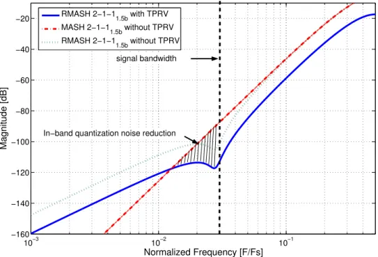
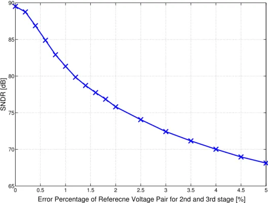
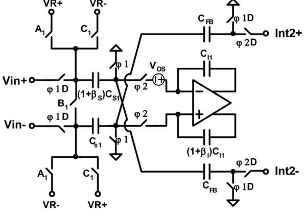
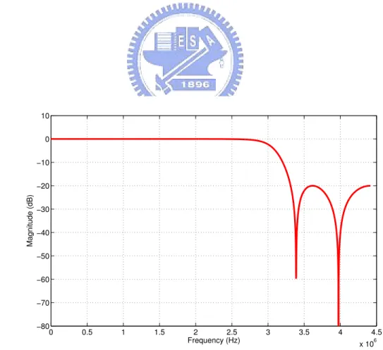
(13) 2.14 Cascaded Σ∆ modulator. . . . . . . . . . . . . . . . . . . . . . . . . . . . . .. 27. 2.15 The output spectrum of MASH 2-2 with finite OTA dc gain and capacitor mismatch. . . . . . . . . . . . . . . . . . . . . . . . . . . . . . . . . . . . . .. 30. 3.1. Signal bandwidth of ADSL2 and ADSL2+. . . . . . . . . . . . . . . . . . . .. 33. 3.2. Maximum date rate of ADSL2 and ADSL2+. . . . . . . . . . . . . . . . . .. 33. 3.3. Dynamic range of a conventional 1.5-bit Σ∆ modulator with L=3, 4, and 5, as a function of OSR. . . . . . . . . . . . . . . . . . . . . . . . . . . . . . . .. 36. 3.4. Resonator-based second-order 1.5-bit modulator. . . . . . . . . . . . . . . . .. 37. 3.5. The block diagrams of (a) RMASH 2-1-11.5b (b) RMASH 2-21.5b . . . . . . . .. 39. 3.6. The nonlinear gain of 1.5-bit and 1-bit quantizer. . . . . . . . . . . . . . . .. 41. 3.7. (a) transfer characteristic and (b) error function of tri-level DAC. . . . . . .. 42. 3.8. The simulated 3rd harmonic distortion of resonator-based modulator with trilevel and single-bit quantizers. (Vth =0.45V, fin=500KHz, OSR=16, fs=70.4MHz) 43. 3.9. The TQN plots of RMASH 2-1-11.5b with TPRVs, MASH 2-1-11.5b without TPRVs, and RMASH 2-1-11.5b without TPRVs. . . . . . . . . . . . . . . . .. 44. 3.10 The peak SNDR versus OSR plots for four different modulators. . . . . . . .. 45. 3.11 The simulated peak SNDR of RMASH 2-1-11.5b with settling error of the low reference voltages, ±0.45V. . . . . . . . . . . . . . . . . . . . . . . . . . . . .. 46. 3.12 The circuit implementation of the first integrator in the first stage of RMASH 2-1-11.5b . . . . . . . . . . . . . . . . . . . . . . . . . . . . . . . . . . . . . . .. 47. 3.13 The block diagram of the three-stage decimation filter. . . . . . . . . . . . .. 48. 3.14 The frequency response of the five-order CIC filter. . . . . . . . . . . . . . .. 48. 3.15 The frequency response of the 31-tap FIR filter. . . . . . . . . . . . . . . . .. 49. 3.16 The frequency response of the fourth-order IIR filter. . . . . . . . . . . . . .. 49. 3.17 Plots of simulated SNDR versus OTA dc gain. (OSR=16) . . . . . . . . . .. 52. 3.18 Plots of simulated SNDR versus 70-dB OTA dc gain and 0.5% capacitor mismatch. (OSR=16). . . . . . . . . . . . . . . . . . . . . . . . . . . . . . . . .. 52. 3.19 OTA-based SC integrator. . . . . . . . . . . . . . . . . . . . . . . . . . . . .. 53. 3.20 Plots of simulated SNDR versus OTA transconductance and output current for RMASH 2-1-11.5b . . . . . . . . . . . . . . . . . . . . . . . . . . . . . . .. 53. 3.21 Plots of simulated dynamic range versus OTA offset voltage. (OSR=16) . . .. 56. 3.22 The plot of the SNDR versus clock jitter for three different structures of the modulator . . . . . . . . . . . . . . . . . . . . . . . . . . . . . . . . . . . . . xiii. 57.
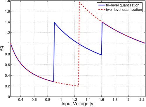
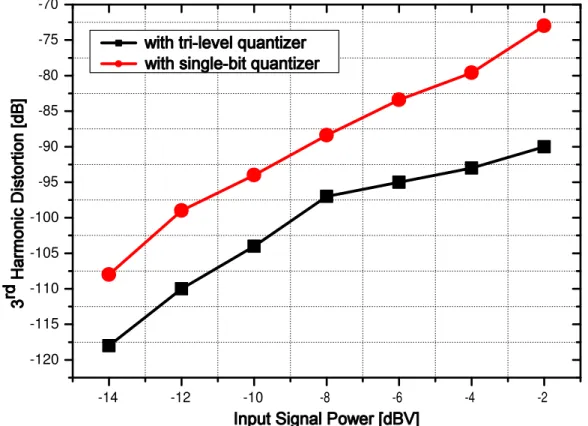
(14) 3.23 The plot of the SNDR versus input sinusoidal frequency for the proposed RMASH 2-1-11.5b (OSR=16) . . . . . . . . . . . . . . . . . . . . . . . . . . .. 57. 3.24 Plots of simulated SNDR versus input level with 30 Monte Carlo analysis runs. 59 3.25 The SC diagram of RMASH 2-1-11.5b . . . . . . . . . . . . . . . . . . . . . . .. 60. 3.26 Non overlapping two-phase clock generator. . . . . . . . . . . . . . . . . . .. 61. 3.27 Circuit schematic of the OTA. . . . . . . . . . . . . . . . . . . . . . . . . . .. 62. 3.28 Circuit implementation of the first-stage modulator. . . . . . . . . . . . . . .. 63. 3.29 Circuit implementation of tri-level quantizer. . . . . . . . . . . . . . . . . . .. 64. 3.30 The schematic of reference voltage buffer amplifier. . . . . . . . . . . . . . .. 65. 3.31 (a) H1 (z) and (b) H2 (z) of Circuit implementation of the cancellation filters. 67. 3.32 Chip micro-photograph. . . . . . . . . . . . . . . . . . . . . . . . . . . . . .. 68. 3.33 The EVM board of test chip measurement. . . . . . . . . . . . . . . . . . . .. 69. 3.34 Plots of measured SNDR and SNR versus input signal level. . . . . . . . . .. 70. 3.35 Measured output PSD of RMASH 2-1-11.5b with DC input. . . . . . . . . . .. 71. 3.36 Measured output PSD of RMASH 2-1-11.5b operating at 80 MHz sampling rate. 71 3.37 Measured output PSD of RMASH 2-1-11.5b operating at 100 MHz sampling rate. . . . . . . . . . . . . . . . . . . . . . . . . . . . . . . . . . . . . . . . .. 72. 3.38 Plots of measured SNDR and SNR versus input signal level. . . . . . . . . .. 72. 3.39 Measured output PSD of proposed RMASH 2-1-11.5b ADC. . . . . . . . . . .. 73. 3.40 (a) FOM distribution of broadband SC Σ∆ modulators with respect to conversion rate, and (b) FOM distribution of wideband SC Σ∆ modulators with respect to area. . . . . . . . . . . . . . . . . . . . . . . . . . . . . . . . . . .. 75. 4.1. The traditional MASH Σ∆ modulators. . . . . . . . . . . . . . . . . . . . . .. 78. 4.2. The conceptual block diagram of the leakage noise removal. . . . . . . . . . .. 80. 4.3. The architecture of proposed single-bit HQCRFF modulator. . . . . . . . . .. 81. 4.4. The simulated Kq of HQCRFF with single-tone input in oscillation mode. . .. 83. 4.5. The simulated Kq of HQCRFF with single-tone input in oscillation mode. . .. 83. 4.6. The frequency responses of NTF, STF, and resonator of HQCRFF. . . . . .. 84. 4.7. The theoretic values and simulated results of input threshold voltage using Equation (4.12) and SIMULINK. . . . . . . . . . . . . . . . . . . . . . . . .. xiv. 85.
(15) 4.8. (a), (b) X[k] and S[k] of HQCRFF with two dynamic amplitudes, -15dB and -30dB of the input sinusoid; (c), (d) X[k] and S[k] with dynamic amplitudes, -15dB, -25dB, -15dB, and -8dB of the input band-limited signal; (e)-(h) The transient behavior of HQCRFF with input sinusoid: The short-time FFTs of HQCRFF outputs for four data intervals, 1∼1024, 513∼1536, 769∼1792, and 1025∼2048 points, respectively; (i)-(l) The transition behaviors of HQCRFF with input band-limited signal: The short-time FFTs of HQCRFF outputs for four data intervals, 1∼256, 257∼512, 513∼768, and 769∼1024 points, respectively. . . . . . . . . . . . . . . . . . . . . . . . . . . . . . . . . . . . . .. 86. The proposed HQCRFF-based MASH 2-0 with RSR technique . . . . . . . .. 88. 4.10 The Block diagram of the proposed RMASH 2-2 architecture . . . . . . . . .. 89. 4.9. 4.11 (a)and (b) are spectra of I(z) and Y (z) of Figure 4.2, respectively. (c) and (d) are spectra of I2 (z) and YRM ASH (z) of Figure 4.10, respectively. The input amplitude is equal to -40dBV. . . . . . . . . . . . . . . . . . . . . . . . . . .. 90. 4.12 (a)and (b) are spectra of I(z) and Y (z) of Figure 4.2(a), respectively. (c) and (d) are spectra of I2 (z) and YRM ASH (z) of Figure 4.2(b), respectively. The input amplitude is equal to -10dBV. . . . . . . . . . . . . . . . . . . . . . . .. 91. 4.13 The output spectra of the MASH 2-0 architectures using: (a) traditional RSR technique [60] and (b) improved RSR technique [61]. . . . . . . . . . . . . .. 93. 4.14 The SNDR as a function of input level for both traditional and proposed MASH 2-0 with RSR technique. . . . . . . . . . . . . . . . . . . . . . . . . .. 94. 4.15 The output spectra of the proposed MASH 2-2 (a) with ideal case, (b) with circuit nonidealities in modulation mode, (c) with ideal case, and (d) with circuit nonidealities in oscillation mode. . . . . . . . . . . . . . . . . . . . . .. 95. 4.16 The two-tone input signal and output of the RMASH 2-2 following a decimation filter. . . . . . . . . . . . . . . . . . . . . . . . . . . . . . . . . . . . . .. 96. 4.17 The SNDR against input level in the proposed MASH 2-2 with Monte Carlo analysis. . . . . . . . . . . . . . . . . . . . . . . . . . . . . . . . . . . . . . .. 96. 4.18 Circuit implementation of HQCRFF 1-bit modulator. . . . . . . . . . . . . .. 98. 4.19 The -35 dBV input signal, integrator output voltages, and 1-bit quantizer output of HQCRFF 1-bit modulator in oscillation mode. . . . . . . . . . . .. 99. 4.20 The -3 dBV input signal, integrator output voltages, and 1-bit quantizer output of HQCRFF 1-bit modulator in modulation mode. . . . . . . . . . . . .. xv. 99.
(16) 4.21 (a) and (b) The SPICE output spectrum of second integrator and 1-bit quantizer of HQCRFF 1-bit modulator with -3dBV input level; (c) and (d) The SPICE output spectrum of second integrator and 1-bit quantizer of HQCRFF 1-bit modulator with -35dBV input level. . . . . . . . . . . . . . . . . . . . . 100 4.22 Circuit implementation of 4-bit LQCIFF modulator. . . . . . . . . . . . . . . 101 4.23 The circuit schematic of 4-bit quantizer. . . . . . . . . . . . . . . . . . . . . 102 4.24 The circuit schematic of comparator. . . . . . . . . . . . . . . . . . . . . . . 102 4.25 The output spectrum of RMASH 2-2 with 290kHz@-3dBV input signal. . . . 103 4.26 The output spectrum of RMASH 2-2 with 290kHz@-35dBV input signal. . . 104 4.27 Plots of SPICE simulated SNDR versus input signal level of RMSAH 2-2. . . 105. xvi.
(17) Chapter 1 Introduction The high performance signal processing in applications such as digital audio, digital subscriber line system, and wireless communication systems has efforts toward improving the performance of data acquisition interfaces. Although the performance increases in the speed and density of integrated circuits due to the advances in VLSI technology, the interfaces between analog and digital systems still limit the speed and resolution. Therefore, it is very important to design a powerful analog-digital converter (ADC) in above applications. As we know, ADCs can be classified into two categories: Nyquist-rate converters and oversampling converters. The principle of Nyquist-rate converters is that they sample analog signals at a rate approximately twice of the maximum frequency of the input signal and they are usually used to digitize wide-bandwidth signals with low to medium resolution such as pipelined ADCs. The other is oversampling converters which sample the analog signal at a rate much higher than the maximum frequency of the input and employ the increase of oversampling ratio (OSR) to produce a high-resolution digital output. Although the Nyquist-rate converters can get the maximum signal bandwidth, the main disadvantage of them is the high sensitivity to component matching and thus they usually can not obtain high resolution. Sigma-Delta (Σ∆) ADCs, which provide a robust and economical solution for highresolution analog-to-digital conversion, have being developed since the 60s of last century [1]. A Σ∆ ADC realizes that the input signals and the corresponding quantization errors pass through the low-pass loop filter and the high-pass filter, respectively. Therefore, the output signals comprise of the delayed input signals and the quantization errors are shaped by the high-order high-pass filter. Theoretically, quantization error can be infinitely shifted out the interesting bandwidth and the conversion resolution can be arbitrarily increased until 1.
(18) the device thermal noise floor physically limits the resolution. Furthermore, Σ∆ ADCs do not require accurate analog component matching to achieve the superior resolution, which makes it suitable for standard CMOS processes. In comparison with the Nyquist-rate ADCs, however, Σ∆ ADCs have to operate at an oversampling frequency, which results in the main drawback: the narrow conversion bandwidth. Recently, more and more research has been focus on development and implementation of Σ∆ ADCs with broad conversion bandwidth [8-10,28-39]. Considering the circuit realization, Σ∆ ADCs can be categorized into discrete-time (DT) structure and continuous-time (CT) structure [2]. Using switched-capacitor (SC) circuits, the DT Σ∆ ADC offers a good degree of accuracy. But the circuit speed is limited by the defective settling of SC integrator. CT Σ∆ ADCs are more adaptive to low supply voltage. The low power dissipation makes the realization of CT ADCs more attractive in future advanced CMOS processes. Input-signal sampling errors, like settling error, charge injection and some other DT problems do not exist in CT circuits. The circuits can operate at a higher speed for a given technology than their DT counterpart. Furthermore, CT Σ∆ ADCs provide implicit anti-alias filtering, thus reducing the need for explicit anti-alias filtering prior to the modulator [3]. But the drawbacks of CT Σ∆ ADCs are serious. A CT Σ∆ ADC requires a highly linear resistor or transconductor, which is not well-suited for implementation in modern sub-micro CMOS processes. Additionally, the pole locations of these integrations are set by the RC (or C/Gm) time constants of these devices. The variation of pole locations determined by products of two different device parameters can be as large as about ±30%. The large mismatch greatly limits the efficacy of CT Σ∆ ADCs without adding elaborate tuning mechanisms. It is also more sensitive to clock jitter [4] and quantizer metastability [5], which cause random pulse width modulation in the feedback DAC. Therefore, they, in turn, cause high-frequency quantization noise to fold into the signal bandwidth, which lowers the conversion resolution [6]. Since the requirement on ADC resolution in high-integration low-cost broadband telecommunication application is normally higher than other applications, this drawback prevents CT Σ∆ ADCs from being a good choice for broadband telecommunication application. Before going into detail in describing the contributions of this work, a short introduction to the analog-to-digital conversion, and to the Σ∆ modulation is given.. 2.
(19) u(t). u(t). u(n). S/H. y(n). fs/2 Figure 1.1: Block diagram of a generic ADC.. Su(f). f S. B. B. S. Figure 1.2: Spectral sampling operation.. 1.1. Analog to Digital Conversion. The conversion of a continuous-time analog signal into a digital one is done in two operations as shown in Figure 1.1. First there is a sampling of the analog signal (usually with a constant sample period Ts ), then a quantization of the signal amplitude is done. If the signal band of a sampled signal is less than half the sampling frequency, the sampling in time is a completely invertible process. Looking at the frequency spectrum of a sampled signal in Figure 1.1 this could be understood. When a signal is sampled at uniform time intervals, this results in a periodicity of the signal spectrum at multiples of the sampling frequency, f S , in the frequency domain as seen in the Figure 1.2. With simple low-pass filtering it is clear that the original baseband spectrum can be reconstructed as long as the spectrums does not overlap. This is achieved when fs ≥ 2fb = fN. (1.1). 3.
(20) where fb is the bandwidth of the input signal. This equation is known as the Nyquist theorem, and fN is called the Nyquist frequency. An analog filter preceding the sampling operation is required to assure that the input signal bandwidth is limited to f b . This filter is known as the anti-aliasing filter (AAF). A basic ADC structure is shown in Figure 1.1. An ADC working at a sampling frequency that equals to fN is called a Nyquist-Rate converter. These converters are hard to design in practice because of the zero transition band required for the AAF. To overcome this problem, this type of converters often use a slight amount of oversampling. The oversampling ratio (OSR) is defined as OSR =. fs fs = . fN 2fb. (1.2). Nyquist rate converters operates in most cases with an OSR = 1.5∼10 [7]. Increasing the OSR greatly relaxes the demands to the AAF, thus simplifies the design and reduces the power and chip area of the filter.. 1.1.1. Quantization. The quantizer encodes a continuous range of analog values into a set of predefined discrete levels. Quantization is usually uniform and the space between two adjacent output levels of the quantizer is defined as the quantizer step size: ∆=. FS −1. (1.3). 2N. where F S is the full-scale input range and 2N is the number of different output levels. Since an infinite number of input values of the sampled input signal is mapped to an finite number of values in the quantizer, the quantization is an noninvertible process. A very useful and important assumption for quantization noise is white. If the input signal x(n) has a rapidly and random variying behavior, the quantization noise e(n) can be approximated as a random number uniformly distributed between ± ∆2 and uncorrelated with its previous values. It is also assumed that e(n) has statistical properties independent of x(n). By these properties, e(n) is classified as white noise with a mean square value of e2rms =. 4. ∆2 12. [2]..
(21) 1.1.2. Oversampling. When using a one-sided representation of the frequency domain, the power spectral density (PSD) of the quanization noise is: Se (f ) =. e2rms. µ. 2 fs. ¶. .. (1.4). Equation (1.4) implies that the quantization noise is uniformly distributed in the frequency range 0 < f < fs /2 . The signal band, however, might have a range from 0 < f < f0 . The total in-band noise power is then calculated by using Equations (1.2) and (1.4): 2 qrms. =. Z. f0. Se (f )df = 0. e2 2f0 e2rms = rms fs OSR. (1.5). Equation (1.5) shows for each doubling of OSR, the in-band noise power decreases by 3dB or 0.5 bits. Data converters employing oversampling to benefit from this property are called oversampled converters. By increasing the OSR they can achieve higher accuracy than Nyquist converters which use the same quantizer.. 1.1.3. Performance Metrics. This subsection reviews the key metrics, such as signal-to-noise ratio, dynamic range, and Nyquist rate, which are needed by the evaluation of the Σ∆ modulator quality. Total harmonic distortion (THD): THD is the ratio between the sum of the power of the higher harmonics, and the power of the fundamental harmonic. Signal-to-noise ratio (SNR): SNR is the ratio in power between the input sine wave fin and the noise of the converter from DC to Nyquist rate. SNR includes all noise sources in the modulator, both thermal and quantization. It is typically expressed in decibels. SN R = 10 log. µ. Psignal Pnoise. ¶. .. (1.6). Signal-to-noise-distortion ratio (SNDR):. 5.
(22) SNDR is similar to SNR, except that it includes the harmonic content. SN R = 10 log. µ. Psignal Pnoise + Pdistortion. ¶. .. (1.7). For small signal levels, distortion is not important. As the signal level increases, distortion degrades the modulator performance, and the SNDR will be less than the SNR. Dynamic range (DR): DR is the ratio in power between the maximum input signal level that the modulator can handle and the minimum detectable input signal. Practically, the maximum input signal level is the input level where the SNDR drops 3 dB beyond the peak. For an ADC, if the signal is too large, it will over-range the ADC input. If it is too small, the signal will get lost in the quantization noise of the converter. Spurious-free dynamic range (SFDR): SFDR is the ratio of the power value of the input sine wave with a frequency fin for an ADC, to the power value of the peak spur observed in the frequency domain. A large spur in the frequency domain may not significantly affect the SNR, but will significantly affect the SFDR. SFDR is a useful metric in communication applications, where the distortion component can be much larger than the signal of interest due to the intermodulation of unwanted interferential signals. Consequently, the small input signals are masked into the spurs; the dynamic range of the ADC is attenuated. Nyquist rate: Nyquist rate fN is the lowest sampling frequency that can be used for analog-to-digital conversion of a signal without resulting in significant aliasing. This frequency is twice the rate of the highest input frequency fb . Therefore, Nyquist rate specifies the minimum sampling frequency required to avoid aliasing.. 1.2. Sigma-Delta ADC. The basic idea of Sigma-Delta (Σ∆) ADC is that it exchanges resolution in amplitude to resolution in time. In such ADC, the analog signal is modulated into a low resolution code at a frequency much higher than the Nyquist rates, and then the excess quantization noise is removed by the following digital filters [2]. Thus, if OSR is high, the oversampling ADCs are very suitable for CMOS VLSI digital technology because it does not require high performance analog buildings. 6.
(23) Loopfilter Lth-Order Loopfilter. X. Y. X(z). E(z) Y(z). H(z) N-bit Quantizer. N-bit Quantizer. D(z). N-bit DAC N-bit DAC. (a). (b). Figure 1.3: Sigma-Delta modulator architecture:(a) Basic block diagram, (b) Corresponding linear model. Figure 1.3 shows the basic block diagram of a Σ∆ modulator and its corresponding linear model. The Σ∆ modulator consists of a feedforward path formed by a Lth-order loopfilter and a N -bit quantizer, and a negative feedback path around them, using a N -bit digitalto-analog converter (DAC). In the linear model as illustrated in Figure 1.3(b), the DAC is assumed to be ideal, D(z)=0, and the injected quantization error, E(z), of the quantizer is assumed as an additive white noise approximation. In this way, the modulator can be considered as a two-input, one-output linear system. Therefore, a signal transfer function (STF) and a noise transfer function (NTF) can be derived: ST F (z) =. H(z) Y (z) = . X(z) 1 + H(z). (1.8). N T F (z) =. 1 Y (z) = . E(z) 1 + H(z). (1.9). In the frequency domain, the output signal is obtained as the combination of the input signal and the noise signal, with each being filtered by the corresponding transfer function: Y (z) = ST F (z)X(z) + N T F (z)E(z).. (1.10). By properly selecting the loop filter, the STF and the NTF of a theoretical Lth-order modulator yield in the z-domain: ST F (z) =. Y (z) H(z) = = z −L X(z) 1 + H(z). (1.11). N T F (z) =. 1 Y (z) = = (1 − z −1 )L E(z) 1 + H(z). (1.12). where H(z) = 1/(1 − z −1 ). Figure 1.4 plots the frequency responses of NTFs with different orders of L. When the loop order is higher than one, the frequency response of NTF. 7.
(24) Figure 1.4: Frequency responses of NTFs with different orders of L presents the characteristic of highpass filters. The higher the order L is, the more quantization error energy is suppressed at low frequencies. For Lth-order loopfilters, a function for approximation of the theoretical in-band noise power is [2]: 2 qrms =. π 2L e2rms (2L + 1)(OSR)2L+1. (1.13). This function is plotted in Figure 1.5. Stability considerations will reduce the practical achievable resolution of higher-order modulators. For higher-order single-bit modulators the difference is substantial (say, more than 60 dB for a 5th-order modulator) [2]. These stability issues arise when the modulator order is higher than second order.. 1.3. Motivation and Contribution. In general, the oversampling converter is used in lower signal bandwidth and highresolution applications such as digital audio. However, due to the requirements of high resolution for modern telecommunication systems (ADSL, VDSL), the increasing resolution and bandwidth of Σ∆ modulators are necessary. Two ways can be used to increase the resolution of Σ∆ modulators. The first one is the increase of the loopfilter order to get better noise shaping. When the high-order Σ∆ modulators are designed, the most important topic is to choose the NTF. In Σ∆ modulator, the more noise is shaping into the out-band. 8.
(25) Figure 1.5: DR versus OSR of a theoretical Sigma-Delta modulator for for different Lth-order (with all zeros at DC). frequency, and the better resolution is obtained. For single-stage Σ∆modulators, additional integrators are placed in the forward path to increase the order of the noise shaping. However, the single-stage Σ∆ modulators are prone to instability if the order is greater than two [2]. Therefore, to design a high-order Σ∆ modulator with stable loopfilter is a very important issue for broadband applications. The second method is the increase of the bit number of internal quantizer to get lower noise floor. The Σ∆ modulators employing multi-bit quantizer can have several advantages over those using the single-bit quantizer [2]. However, the major problem in designing the multi-bit sigma-delta modulators is that much better component matching for the internal DAC linearity is required. Therefore, the performance of the multi-bit Σ∆ modulators is directly related to the linearity of the internal multi-bit DAC in the feedback path. Although, there are various innovative multi-bit DAC architectures employing dynamic element matching (DEM) to improve the linearity of the internal DAC, most of them will increase the analog circuit complexity. To be compatible with the telecommunication applications, this thesis describes two cascaded high-order Σ∆ modulators to achieve high DR at low OSR. The first one is a cascaded 2-1-1 modulator with an OSR of 16 and a signal bandwidth of 2.2 MHz suited for ADSL2+. The key features of this cascaded modulator are the use of 1.5-bit quantizer/DAC in each stage and the use of two pairs of reference voltages. The second one is a resonatorbased cascaded modulator with an intrinsic oscillation mode which can be used to improve DR. 9.
(26) 1.4. Thesis Organization. This thesis consists of five chapters, of which that is the first. Chapter 2 provides a architecture survey of Σ∆ modulators that are suited for broadband applications. The broad bandwidth (>1 MHz) usually implies some trends and limitations of architecture design. Firstly, the OSR must be reduced to avoid the high sampling frequency. Secondly, the orders of loopfilter should be increased to maintain desired DR by using aggressive noise shaping. Finally, the multi-bit internal quantizers and multi-bit feedback DACs may be used to increase DR and to provide good stability of the loopfilters. Among existed architectures, three architectures are most possible candidates for broadband applications. They are continuous-time Σ∆ modulator, single-loop Σ∆ modulator, and cascaded Σ∆ modulator. The basic characteristic of each architecture are addressed as well as some major design limitations and challenges are discussed. Chapter 3 describes the proposed fourth-order cascaded modulator for ADSL2+ application. Three architectural features are involved in the proposed modulator. They are the use of 1.5-bit quantization, the use of bandpass noise shaping, and the use of two different pairs of reference voltages. The detailed architectural analysis and circuit implementation are addressed. The modulator is fabricated in a 0.25-µm CMOS technology, in a 2.8-mm 2 active area including decimation filter and reference voltage buffers, and dissipates 180 mW from a 2.5-V power supply. As shown in the experimental result, for a 2.2 MHz signal bandwidth, the ADC achieves a dynamic range of 86 dB and a peak signal-to-noise and distortion ratio (SNDR) of 77 dB with an oversampling ratio of 16. Chapter 4 presents a new resonator-based cascaded architecture, called RMASH, for lowOSR Σ∆ modulators. Based on two resonator topologies, the architecture can be immune to leakage quantization noise caused by circuit nonidealities over a large portion of the input range when OSR is low, and hence the DR can be improved. The key of improving DR is to use a cascade-of-resonator-with-feedforward modulator in the first stage and a low-Q cascade-of-integrator-with-feedforward in the following stage. The first stage can operates in the modulation mode or the oscillation mode depending on the input amplitude. When the first stage oscillates, the leakage quantization noise problem can be alleviated. The theoretic analysis of operating condition for oscillation mode is presented and the transient behavior between two modes is also discussed. Finally, the design methodology and simulation result of RMASH are addressed. As can be seen from the simulation results, without using additional calibration techniques, the DR of the proposed RMASH 2-2 architecture with the op-amp 10.
(27) dc gain of 60 dB, the capacitor mismatch of 0.2%, and the OSR of 8 can be as high as 84 dB. Chapter 5 begins with a summary which concludes the results achieved in this thesis. Also some issues are brief discussed for future work.. 11.
(28) Chapter 2 Architecture Survey Σ∆ modulators have been notably employed to implement high-resolution analog-todigital conversions (ADCs) or digital-to-analog conversions (DACs) for narrow bandwidth applications such as voice-band telecommunications and audio signal acquisitions in the last decade. One of the most important reasons is that they make the realization of highresolution data converters possible while requiring only moderate-quality analog components. The performance of a Σ∆ modulator is mainly determined by the performance of the analog building blocks whose specifications are dictated by the selected architecture. Therefore it is important to select the best suitable architecture that relaxes the circuit specifications while keeps the desired performance. With the increasing demand of Σ∆ modulator with broader bandwidth and higher dynamic range (DR), the architectures with low oversampling ratio (OSR) becomes more and more attractive. For this reason this chapter surveys possible architectures which are suited for low OSR applications. There are many architectures to implement a Σ∆ modulator and three architectures are most popular choices for high-DR and low-OSR applications among them. They are continuous-time, discrete-time single-loop, and discrete-time cascaded modulators. In the following subsections, the architectural characteristic and design challenge of these architectures are addressed.. 2.1. Continuous-Time Σ∆ Modulator. The exist and implementation of continuous-time (CT) Σ∆ modulator have been a long time. Due to the coming of switched-capacitor (SC) circuits in the 1980s, the majority of Σ∆ modulator have been implemented by SC loopfilters referred as discrete-time (DT) modula-. 12.
(29) tors. This development comes from the fact that SC filters exhibit both good accuracy and good linearity. Furthermore the transfer function of a SC filter is independent of clock rate. In contrast, CT filters usually have poor linearity and accuracy. The time-constants of the CT filter suffer from large variation and typically require calibration. Recently, Σ∆ modulators utilizing CT loopfilters become more and more attractive because of three important reasons [2]: 1). CT modulators have inherent anti-aliasing property. The use of CT loopfilter postpones the unavoidable sampling of the signal to the output of the loopfilter. Thus, imperfections of the sampling process and the folding of the wideband noise have the same degree of suppression to that of quantization noise suppression. This inherent anti-aliasing relaxes the requirement of anti-aliasing filters, which typically must precede the SC modulators. 2). CT modulators potentially can operate in high sampling frequency. The theoretical limit on the sampling frequency of a CT modulator is determined by the regeneration time of the quantizer and the update rate of the feedback DAC, whereas in an SC modulator the sampling frequency is limited by the opamp settling performance dominated by the unitygain frequency of the amplifiers within it. As a result, the CT modulator can operate with a clock frequency which is 2-4 times faster than that which can be achieved with SC loopfilters. This increases the achievable signal bandwidth of CT modulators in spite of lower linearity and accuracy. 3). CT modulators have the advantage of low power dissipation. In contrast to an SC design, in a CT loopfilter there is no need for fast settling integrators. Hence, in a CT loopfilter, the bandwidth requirements of the sub-blocks (opamps, or Gm-C cells) are more than three times lower compared to an SC loopfilter. The above three advantages make the development of CT modulators benefit from the broadband applications [8, 9, 10]. However, the feedback loop delay and timing jitter usually limits the achievable performance.. 2.1.1. Excess Loop Delay. Ideally DAC currents respond immediately to the quantizers clock edge, but the nonzero transistor switching time of the latched comparator and the DAC result in a finite delay between the comparator and the DAC [11]. This delay is called ”Excess Loop Delay”. Excess loop delay can be modeled as td = ρd · T as depicted in Figure 2.1 for an non return to zero (NRZ) DAC pulse. ρd is dependent on the switching speed of the transistors ft , the quantizer 13.
(30) V. V. T. t. td. (a). T+td t. (b). Figure 2.1: Excess loop delay: (a) ideal DAC pulse, (b) delayed DAC pulse. clock fs , the number of transistors in the feedback path nt , as well as the loading on each transistor, and a rough approximation is ρd ≈. n t fs ft. [11]. This excess loop delay increases the. noise floor for a given Σ∆ modulator [11] since this noise adds to the quantization noise of the Σ∆ modulator and is shaped by the noise transfer function. The excess loop delay also potentially increases the instability of the Σ∆ modulator by adding another order to the loop filter [12]. The detailed analysis of excess loop delay for a CT modulator can be found in [11, 12]. Here a fifth-order 1-bit CT modulator with OSR of 32 is used to evaluate the effect of excess loop delay as shown in Figure 2.2. Assuming that the excess loop delay is 0.1% of the sampling period 10ns, the output spectrum of the modulator is shown in Figure 2.3. According to Figure 2.3, the excess loop delay increases not only the noise floor but also the instability of the modulator loopfilter.. 2.1.2. Clock Jitter. Clock jitter is statistical variations of clock edges [13]. Two clocks are present in a CT Σ∆ modulator and both can be affected by clock jitter. One of the clocks controls the decision instant of the quantizer while the other clock controls the DAC output. Since the output of the quantizer is shaped by the NTF, the impact of this error will be relatively small. Conversely, the output of the DAC is shaped by the STF since this signal adds to the input signal, and thus the impact of this error will affect the baseband noise in the Σ∆ modulator [14]. There are two varieties of clock jitter, delay clock jitter and pulse-width clock jitter. Paper [15] demonstrates that in a second-order Σ∆ modulator, the delay clock jitter is shaped by the NTF while the pulse-width clock jitter manifests itself as white noise. This jitter noise degrades the SNR of the Σ∆ modulator more severely since the white noise spreads evenly across the frequency spectrum. Therefore the clock jitter discussed will be. 14.
(31) 15. Figure 2.2: The simulink model of a fifth-order 1-bit CT modulator with excess loop delay. a1 Gain1 a2 Gain2. a3 Gain3 a4 Gain8 a5 Gain7. yc Saturation2Sign. 0.5 Signal Generator. (1/fs)s Transfer Fcn. 0.5 1−z−1 Saturation. 0.5 1−z−1. Discrete FilterSaturation1. 0.5 1−z−1. Discrete Filter1Saturation3. 0.25 a6 1−z−1 Saturation4 Discrete Filter2 Discrete Filter3Saturation5 Gain5 Gain6 g2. g1. b. Gain Transport Delay. Gain4. Unit Delay 1 z. Zero−Order Hold. To Workspace.
(32) 0. Output spectrum of 5th 1−bit CT Σ ∆ modulator with an OSR of 32 without excess loop delay@SNDR=80dB with 0.1% excess loop delay@SNDR=39dB. −20. PSD [dB]. −40. −60. −80. −100. −120. −140 −4 10. −3. 10. −2. 10. Normalized Frequency [F/Fs]. −1. 10. Figure 2.3: The output spectra of the fifth-order 1-bit CT modulator with and without excess loop delay the pulse-width clock jitter incurred in the DAC. DT Σ∆ modulators are relatively insensitive to pulse-width clock jitter because they are utilized by SC circuits. The insensitivity is due to the sloping pulse form of the feedback [13]. Since most of the charge transfer in a SC circuit occurs at the beginning of the clock period, clock jitter introduces a minimal amount of error in the charge lost ∆Q D as shown in Figure 2.4(a). The capacitor is discharged over a switch with very low on-resistance, thus reducing the value of τ = RC and causing a fairly steep slope as the DAC discharges [5]. In contrast, CT Σ∆ modulators transfer charge at a constant rate over the clock period, and thus the charge loss ∆QC due to a timing error is proportionally much greater than that of the DT Σ∆ modulator as shown in Figure 2.4(b). Assuming white clock jitter, the sampling times of the output bits (for a sampling period T) are given by tn = nT + ∆t 2 where ∆t is an independent and identically distributed random variable with variance σ ∆t .. The resulting noise power of the clock jitter for a 1-bit quantizer with a step size of ∆ and a typical return-to-zero (RZ) DAC pulse is given by [13] Pj =. 2 ∆2 σ∆t OSR · T 2. (2.1). 16.
(33) Figure 2.4: (a) Clock jitter in DT modulator. (b) Clock jitter in CT modulator.. 17.
(34) The quantization noise power of a general Lth order Σ∆ modulator is given by [2] Pq =. ∆2 π 2L (24L + 12) · OSR(2L+1). (2.2). An figure of merit for the noise can be defined as the point at which the noise power of the clock jitter is equal to the noise power of the quantization noise, thus reducing the SNR by 3dB [13]. Equating (2.1) and (2.2), this critical value is found to be πL σ∆t p = T (24L + 12) · OSRL. (2.3). This value decreases with increasing OSR, meaning that as the OSR increases the clock jitter becomes more detrimental. Also, as the order of the modulator is increased,. σ∆t T. decreases,. indicating that proportionally the clock jitter becomes more significant in higher order CT Σ∆ modulators.. 2.2. Single-Loop Σ∆ Modulator. The single-loop architecture means the modulator has only one conversion stage and one quantizer. In [2], it has been shown that OSR, loopfilter order, quantizer bit are related to the DR of the Σ∆ modulator by 3 DR = 2. µ. 2L + 1 π 2L. ¶. (2N − 1)2 OSR2L+1 .. (2.4). where L is the order of loopfilter and n is the bit number of quantizer. This equation is valid only for the case of pure-differentiation NTF, e.g. N T F = (1 − z −1 )L . For the case of L ≤ 2, its prediction is exact. However, the stability considerations usually present the such NTF being implemented when L ≥ 2. As a result, the achievable DR in the case of L ≥ 2 is usually lower than that predicted by Equation (2.4). The higher the order, the worse the degradation becomes especially when 1-bit quantizer is used. As a result, the highorder multi-bit structures are usually the best choice for single-loop low-OSR modulators. There are two general structures to implement the high-order single-loop modulators called feedforward (FF) and feedback (FB). The main difference between FF and FB structures is that in the FB structure, the quantizer output is fed back to the input of each integrator. In the contrast to FB, the quantizer output of FF structure is fed back only to the input. 18.
(35) b1. b2. X(z) g1H(z). g2H(z). g3H(z). a1. g4H(z). a2. a3. a4. quantizer Y(z). DAC. Figure 2.5: The block diagram of FF fourth-order single-loop modulator. stage. According to analysis of [16], the single-loop modulator with FF structure is preferred for broadband applications. Thus, the FF structure is selected to be the design example of high-order single-loop modulators. The readers who interest in FB structure can refer the articles [2].. 2.2.1. Feedforward Structure. When a high-order sigma-delta modulator is designed, the NTF is the main considered condition because it decides the performances of the modulator. Generally, the NTF of an even-order FF sigma-delta modulator can be expressed as. N T F (z) = Q m. i=1. m Q. i=1. [(1 − z −1 )2 + bi ] +. m P. i=1. [(1 − z −1 )2 + bi ]. ([a2i−1 (1 − z −1 ) + a2i ]. m Q. j=i+1. (2.5) [(1 − z −1 )2 + bj ]). The NTF determines what extent the quantization noise is reduced in a given bandwidth and hence determines the overall signal-to-noise ratio (SNR) of the converter. The feedback coefficients may decide the zeros and the feedforward coefficients decide the poles. There are several design tools for automatic coefficients synthesis of high-order loopfilter [16, 2]. One of them is called ”DELTA-SIGMA TOOLBOX”, which is made by Richard Schreier [2]. This toolbox is programmed by MATLAB and the reader can obtain your free copy of it from the MathWorks web site [17]. In order to get more sight, two sample design 19.
(36) NTF poles and zeros of four−order 1−bit modulator. 1 0.8 0.6 0.4 0.2 0 −0.2 −0.4 −0.6 −0.8 −1. −1. −0.5. 0. 0.5. 1. Figure 2.6: The locations of NTF poles and zeros for FF fourth-order 1-bit modulator. examples of fourth-order 1-bit and 4-bit modulators synthesized by this tools are provided. The block diagram of FF fourth-order single-loop modulator is shown in Figure 2.5. Given the OSR of 32 for the fourth-order 1-bit modulator, the NTF can be synthesized by using the ”synthesizeNTF ” function and the results is given as N T F1−bit =. (1 − 1.999z −1 + z −2 ) · (1 − 1.993z −1 + z −2 ) (1 − 1.49z −1 + 0.563z −2 ) · (1 − 1.7z −1 + 0.7861z −2 ). (2.6). Note that the maximum out-of-band gain of the NTF of 1-bit modulator is set to be 1.5 according to the Lee’s rule (say, L < 2). Figure 2.6 shows the locations of NTF poles and zeros. By adding the small negative-feedback terms, b1 and b2 , around pairs of integrators in the loopfilter as shown in Figure 2.5, the zeros are distributed through the signal band in order to lower the in-band noise [18]. The poles are chosen to flat the frequency response at high frequency in order to reduce the high-frequency noise. It is possible to move the open-loop zeros away from dc along the unit circle by using a feedback loop around pairs of integrators in the loopfilter. This approach is especially useful for broadband or lowOSR applications because the in-band quantization noise can be suppressed. The frequency response of NTF is shown in Figure 2.7. Obviously, the in-band NTF zeros result in the notch filtering, thus causing a flat shape in the signal band. The rms gain of NTF in the signal. 20.
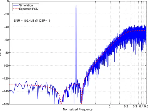
(37) NTF Frequency Response. 10 0 −10 −20. Magnitude [dB]. −30 −40 −50 −60 −70 −80 −90 −100 0. 0.05. 0.1. 0.15. 0.2 0.25 0.3 Normalized frequency [F/Fs]. 0.35. 0.4. 0.45. 0.5. Figure 2.7: The frequency response of NTF for FF fourth-order 1-bit modulator. band is approximatly -59dB. The simulated and expected power spectrum density (PSD) of fourth-order 1-bit modulator by using the ”simulateDSM ” function is shown in Figure 2.8. The predicted and simulated SNDR versus input level is shown Figure 2.9. According to Figure 2.9, the peak SNDR of fourth-order 1-bit modulator with OSR of 32 is 79.2dB which is less than 14-bit resolution. To further increase the peak SNR, the higher order or OSR is required at the expense of increasing the silicon cost and power dissipation. The fourth-order 4-bit modulator with OSR of 16 has the similar design flow to 1-bit one, but benefits from the more stable gain of the quantizer, because the better the gain of the quantizer is known, the more stable is the loop and more aggressive can be the noise shaping. As a result the maximum out-of-band gain of the NTF is increased to be 5, which greatly enhances the resolution of the modulator. The synthesized NTF of fourth-order 4-bit modulator is given as N T F4−bit =. (1 − 1.996z −1 + z −2 ) · (1 − 1.971z −1 + z −2 ) (1 − 0.6214z −1 + 0.1142z −2 ) · (1 − 0.49z −1 + 0.3385z −2 ). (2.7). The simulated and expected PSD of fourth-order 4-bit modulator is shown in Figure 2.10. while the simulated SNDR versus input level is shown Figure 2.11. According to Figures 2.10 and 2.11, the modulator achieves peak SNR of 107.7dB which is larger than 17-bit. 21.
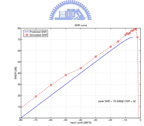
(38) Output Spectrum. 0 Simulation Expected PSD −20 SNR = 77.5dB @ OSR = 32 −40. dBFS. −60. −80. −100. −120. −140 −3 10. −2. 10. −1. Normalized Frequency. 10. Figure 2.8: The simulated and expected power spectrum density (PSD) of fourth-order 1-bit modulator.. SNR curve. 80 Predicted SNR Simulated SNR 70. 60. SNDR [dB]. 50. 40. 30. 20 peak SNR = 79.2dB@ OSR = 32 10. 0 −80. −70. −60. −50. −40 −30 Input Level [dBFS]. −20. −10. 0. Figure 2.9: The predicted and simulated SNDR versus input level of FF fourth-order 1-bit modulator.. 22.
(39) Output Spectrum. 0 Simulation Expected PSD −20 SNR = 102.4dB @ OSR=16 −40. dBFS. −60. −80. −100. −120. −140. −160 Normalized Frequency. 0.1. 0.2. 0.3 0.4 0.5. Figure 2.10: The simulated and expected power spectrum density (PSD) of fourth-order 4-bit modulator. Table 2.1: Coefficients of fourth-order 4-bit CIFF modulator with an OSR of 16. Coefficient a1 a2 a3. Value Coefficient 2.8886 a4 3.3902 b1 1.8321 b2. Value 0.3220 0.0044 0.0283. resolution. In order to convert the NTF into a set of coefficients for a particular topology, the ”realizeNTF ” function is used. Considering the cascade-of-integrators, feedforward form (CIFF) as shown in Figure 2.5, the resulting set of coefficients is listed in Table 2.1. Although the fourth-order 4-bit modulator has higher peak SNR and lower OSR compared with 1-bit one, a notable limitation of this modulator is that the linearity of the feedback DAC is not perfect. We can model the nonlinearities in an ADC system as additive noise sources as shown in Figure 2.1. The quantizer is replaced by two additive noise sources. The one labeled E(z) represents the quantization errors of an ideal converter and D(z) represents the errors due to the deviation of the internal DAC outputs from their ideal values. For noise shaping, the gain of must be large at low frequencies. Therefore, both quantization errors E(z) is reduced by this large gain when they are referred back to the input X(n). However, the nonlinearity of the internal DAC, D(n), resides in the feedback path where its nonlinearities due to mismatches in levels are not reduced by the negative feedback. The 23.
(40) SNR curve. 110 Simulated SNR 100 Peak SNR = 107.7dB@ OSR = 16 90 80. SNR [dB]. 70 60 50 40 30 20 10 0 −110. −100. −90. −80. −70. −60 −50 Input Level [dBFS]. −40. −30. −20. −10. 0. Figure 2.11: The simulated SNDR versus input level of FF fourth-order 4-bit modulator. mismatch of the N-bit internal DAC will thus become an important factor of nonlinearity to whose ADC system.. 2.2.2. Dynamic Element Matching. Element mismatches in the multi-bit feedback DAC introduce an output error, which consists of the harmonics of the input signal as well as an increased noise floor due to the folding of high-frequency quantization noise into the signal band. In some cases, the increased noise floor is acceptable, but the harmonic distortion is not. Thus, the dynamic Element matching (DEM) is a circuit technique for the randomization of the static nonlinearity of the DAC by converting the energy of the harmonic spurs into pseudo-random noise [19]. The concept of DEM for a parallel-unit-element DAC is shown in Figure 2.12 where the N th output level is generated by connecting N unit elements to the output summing node. Since the error term ∆Ei of unit element Ei is only approximate but not exactly equal, two different output levels can be obtained by closing switches S1 , S2 and S1 , S3 namely, 2E + ∆E1 + ∆E2 and 2E + ∆E1 + ∆E3 . In a multi-bit DAC without DEM, always the same set of switches are closed to implement the same output level while the DAC with DEM the sets of switches are changed dynamically controlling a given DEM algorithm. Then the DAC error will not be correlated with the value of is input, and hence the signal distortion 24.
(41) Figure 2.12: DAC with dynamic element matching linearization. is replaced by random noise in the DAC output. To illustrate the effect of DEM, Figure 2.13 compares the output spectrum of a third-order CIFF modulator with a 3-bit quantizer and a fixed OSR of 32, without and with DEM. A ±1% linear-gradient mismatch is applied to the unit elements of the 3-bit feedback DAC. Accordingly, the DEM eliminates the large harmonic spurs caused by the DAC mismatch. However, as shown in Figure 2.12, DEM techniques requires some digital signal processing between the output of the quantizer and the input of the DAC. This causes an additional delay in the feedback path, thus limiting the maximum sampling frequency. Since DEM techniques improve DAC linearity by the use of noise shaping, this improvement strongly depends on the capability of noise shaping namely OSR and loopfilter order. Broadband Σ∆ modulators require low OSR therefore the shaping capability have to maintain by increasing the loopfilter orders. The higher the order of the loopfilter, the higher complexity and delay of the DEM algorithms is. As a result, it turns out that in the case of low OSR and broadband applications, the modulator performance and DEM complexity becomes a trade-off. There are serval improved versions of DEM techniques were proposed for broadband Σ∆ modulators, such as data-weighted average (DWA) [20, 21, 22], Bi-DWA [34], individual level averaging (ILA) [23], digital correction or calibration [24, 25]. All of 25.
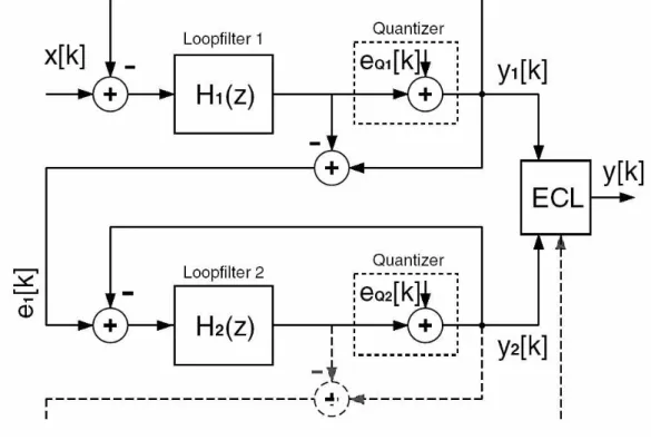
(42) 0. Output spectrum of 3rd CIFF Σ ∆ modulator with a 3−bit quantizer with DEM@SNDR=88dB without DEM@SNDR=60dB. −20. PSD [dB]. −40. −60. −80. −100. −120. −140 −3 10. −2. −1. 10. Normalized Frequency [F/Fs]. 10. Figure 2.13: The output spectrum of a third-order 3-bit CIFF modulator with and without DEM. these techniques require additional circuities and power dissipation.. 2.3. Cascaded Σ∆ Modulator. The main difference between the cascaded and the single-loop Σ∆ modulator is the number of conversion stages. The single-loop modulator has only one conversion stage, while the cascaded modulator has more conversion stages. Figure 2.14 shows a block diagram of a possible implementation; several single-loop modulators can be seen, where each stage takes the error of the previous quantizer and digitizes it. The output streams are then combined in the error correction logic (ECL) in such a way that each quantization error e Qi [k], but the one generated in the last stage, is cancelled. The result of this exercise is that, if every operation is exact, the remaining noise is shaped with an order equal to the sum of the orders of the employed loopfilters. Compared with single-loop high-order modulator, cascaded one, instead, do not need loops with L > 2 to achieve higher-order noise shaping. Hence, they have better stability and they usually reach higher DR at similar OSR, n, and L conditions. In addition, the architectures with cascaded loops also take advantage of the fact that the quantization noise is reduced when the residual error of an internal quantizer is amplified, before being converted by the following stage. The final DR is actually increased by the gain. 26.
(43) Figure 2.14: Cascaded Σ∆ modulator. itself and may even exceed the value given by Equation (2.4).. 2.3.1. Leakage Quantization Noise. Unfortunately the cascaded modulator requires a very accurate NTF of the first stage putting high specifications on the analog building blocks. The biggest problem of cascaded modulators is their sensitivity to mismatch between analog and digital circuities. In singleloop modulator a mismatch between the realized transfer function and the ideal designed filter degrades the stability of the loop. Nevertheless, it has been observed that coefficients variations of up to 20% and large integrator leakage, caused by amplifier finite gain can still be tolerated without a noticeable loss in performance. In contrast,the finite opamp dc gain and capacitor mismatch reshape the STF and NTF of a cascaded modulator and hence degrade the modulator performance. In order to explain the sensitivity of the cascaded modulator to the NTF accuracy, the operation of a cascaded 2-2 modulator (MASH2-2) is described. The block digram of MASH 2-2 can be referred as Figure 2.14 where H1 (z) and H2 (z) are second-order loopfilters. Assuming that the perfect match between the N T F 1 (z) (the first-stage NTF) and error correction logic ECL(z) the output of the MASH 2-2 can be. 27.
(44) given by: YM ASH2−2 (z) = z −2 X(z) + d1 ECL(z)N T F2 (z)Emb (z). (2.8). where X(z), Esb (z), and Emb (z) represent the input signal, 1-bit quantization noise, and multi-bit quantization noise, respectively. In the ideal analysis, the dc gain of the op-amp is assumed to be infinite. However, this assumption is impossible to be achieved due to circuit limitations. In the presence of a finite-gain op-amp, the transfer function of a leaky integrator can be expressed as follows: [2] I(z) =. az −1 1 − (1 − µ)z −1. (2.9). where where µ denotes the inverse open-loop gain A0 of the op-amp, and a is the integrator scaling factor. Based on Equation (2.9), the numerator of the NTFs can be approximately given by N T F2nd (z) ≈ (1 + 2µ)(1 − z −1 )2 + µ(˜ a1 + a ˜2 )(1 − z −1 ). (2.10). where the coefficients a ˜1 and a ˜2 are two cumulative scaling factors of integrators. Thus, the resulting output noise powers of a second-order 1-bit modulator can be written as: P2nd. · 4 ¸ 2 π ∆2sb 1 −5 2 2π −3 OSR + µ (˜ a1 + a ˜2 ) OSR . ≈ 12 (a1 a2 )2 5 3. (2.11). Assuming a typical MASH 2-2 uses the multi-bit quantizer in the second stage, the output quantization noise power can be approximately given by: PM ASH2−2 ≈ +. ∆2sb 1 12 (a1 a2 )2. ∆2mb 1 12 (a3 a4 )2. h. π4 OSR−5 5. 2. + µ2 (˜ a1 + a ˜2 )2 π3 OSR−3 h 8 i π −9 2 2 π6 −7 OSR + µ (˜ a3 + a ˜4 ) 7 OSR . 9. i. (2.12). where ∆sb and ∆mb represent the separation of the 1-bit and multi-bit quantizers for the first and second stages, respectively. According to Equation (2.12), the finite opamp gain arises the quantization noise power and thus degrades the achievable peak SNR. Generally, the integrator gain can be achieved by the capacitor ratio in an SC modulator and thus capacitor mismatch affects the modulator performance due to the change of the. 28.
(45) NTF. In the cascaded multi-bit modulator, however, the capacitor mismatch not only changes the NTF, but also leaks the single-bit quantization noise to the final modulator output. We first define the gain error of the integrator gain as: a01 = a1 (1 − εa1 ). (2.13). The epsilon represents the relative error of the analog coefficients, and can be calculated as: εa1. ∆a01 = a1. (2.14). Substituting Equation (2.14) in Equation (2.8) yields the following modulator output: YM ASH2−2 (z) ≈ z −2 X(z) + d1 H2 (z)N T F2 (z)Emb (z). (2.15). +(1 − z −1 )2 (1 − εg )Esb (z). where 1 − εg = (1 − εa1 )(1 − εa2 ). It is observed that the 1-bit quantization noise appears at the modulator output and dominates the total in-band noise power due to the lower order noise shaping. Taking the finite op-amp dc gain, capacitor mismatch and DAC error into account, combining Equations (2.12) and (2.15), the in-band power for the MASH2-2 can be approximated as: PM ASH2−2 ≈ +. ∆2sb 1 12 (a1 a2 )2. ∆2mb. 1 12 (a3 a4 )2. h. h. π4 OSR−5 5. π8 9. + (1 −. 4 εg )2 π5 OSR−5. OSR−9 + µ2 (˜ a3 + a ˜ 4 )2. π6 7. 2. + µ (˜ a1 +. OSR−7 + σD2. π4 5. 2 a ˜2 )2 π3 OSR−3. OSR−5. i. i. +. (2.16). where σD represents the power of the DAC error in the feedback path. The presence of leakage quantization noise from the 1-bit quantizer, the last term in Equation (2.16), limits the achievable resolution of the MASH 2-2 modulator. Figure 2.15 shows the output spectra of a MASH 2-2 modulator with 1-bit and 4-bit quantizers in the first and second stages respectively where the 60dB OTA dc gain and 0.1% capacitor mismatch are assumed. Obviously, the leakage noise seriously degrades the performance of cascaded modulator for low-OSR application.. 29.
(46) 0. PSD [dB]. −50. −100. −150. −200 Ideal case@SNR=89dB Nonideal case@SNR=68dB −250 −3 10. −2. −1. 10. Normalized Frequency [F/Fs]. 10. Figure 2.15: The output spectrum of MASH 2-2 with finite OTA dc gain and capacitor mismatch.. 2.4. Summary. In Section 2.1 the CT modulator have been introduced and its architectural characteristics are also reviewed. The CT modulator has good potentiality for broadband applications since their sampling clock rate are usually three times faster compared to a DT solution. However, the variation of RC time constant, clock jitter, and excess loop delay of the CT modulator seriouly degrades the performance, thus limiting the achievable DR. The DT modulator can be divided into two parts based on their loopfilter types, singleloop architecture and cascaded architecture. The single-loop high-order modulators with have been widely applied to broadband applications because of having lower sensitivity to the finite dc gain of opamps and capacitor mismatch. However, the instability of singleloop high-order modulators with 1-bit quantizer limits their capability of noise shaping, thus resulting in a poor SNR for broadband applications. The single-loop high-order modulators with multi-bit quantizer not only relax the instability of loopfilter but also increase the achievable DR. However, the distortion caused by multi-bit feedback DAC degrades the SNDR. It is unacceptable for broadband telecommunication applications. Several circuit techniques have been proposed to reduce the distortion caused by multi-bit feedback DAC at the expense of increasing circuit complexity and power dissipation. The cascaded modulators combine serval low-order stages in the ECL to generate the desired high-order NTF. Since no high-order loopfilter is used, they have better stability 30.
(47) and they usually reach higher DRs compared with single-loop ones. However, cascaded modulators are sensitive to the finite dc gain of opamps and capacitor mismatch due to the leakage quantization noise in the ECL output. Thus, the performance degradation strongly depends on the specifications of analog building blocks, which increases the circuit design challenges. This degradation becomes worse when the OSR is low and the multi-bit quantizer is used in last stage. Although some digital calibration techniques can reduce leakage quantization noise, they usually require complex digital processing. The next two chapters will describe two new cascaded modulators for broadband telecommunication applications. The first one is a cascaded 2-1-1 modulator with 1.5-bit quantizer to achieve high DR and low OSR for the newly asymmetric digital subscriber line (ADSL2+) standard. The architectural analysis, circuit implementation, and experiment result will be given. The second one is a resonator-based cascaded modulator in which a new operating principle is present to improve the DR loss caused by leakage quantization noise. The theory analysis, architecture design, and simulation results will be addressed.. 31.
(48) Chapter 3 A Fourth-Order Cascaded Σ∆ ADC for ADSL2+ Application Asymmetric digital subscriber line (ADSL) technology can use the plain old telephone service (POTS) consisting of the existing telephone lines, on-site transceivers and shared exchange multiplexers to deliver high-rate digital data [26]. Since the POTS has different degree’s of quality and different lengths, a new modulation technology called Discrete Multitone (DMT) is used to allow the transmission of high speed data. Such transmission is paid with an increased accuracy in the detection of the modulated signals, which requires analog-to-digital converters (ADCs) with a resolution in the range of 13-15 bits. Today, the newly released ADSL standard called ADSL2+ is a double frequency band version of ADSL2 [27]. The ADSL2+ system increases the frequency ranges on the transmission line from 1.1 MHz to 2.2 MHz as shown in Figure 3.1. This has the potential to increase the short-loop data transmission rate up to 26 Mbps (downstream) as shown in Figure 3.2 [27]. Although ADSL2+ provides higher data rates, it increases the design challenge of the ADCs in the analog front-ends (AFEs). High resolution and broad bandwidth are not only requirements for an ADSL2+ ADC. The power dissipation is also an issue since the limited available energy in mobile device or in the powered modems. Thus, how to choose the ADC architecture for optimizing the trade-off among power, resolution and bandwidth becomes a key issue. Pipelined and Σ∆ converters, among the existing ADC architectures, are most suitable candidates to meet the requirements of ADSL2+ standard. Generally speaking, pipelined ADCs can achieve broad bandwidth, but have limited dynamic range (DR), high power dissipation, and large silicon area. On the other hand, the state-of-the-art Σ∆ ADCs can achieve high DR and wide bandwidth with noise shaping and oversampling techniques. Pa32.
(49) Figure 3.1: Signal bandwidth of ADSL2 and ADSL2+.. Figure 3.2: Maximum date rate of ADSL2 and ADSL2+.. 33.
數據
+7
相關文件
• helps teachers collect learning evidence to provide timely feedback & refine teaching strategies.. AaL • engages students in reflecting on & monitoring their progress
Robinson Crusoe is an Englishman from the 1) t_______ of York in the seventeenth century, the youngest son of a merchant of German origin. This trip is financially successful,
fostering independent application of reading strategies Strategy 7: Provide opportunities for students to track, reflect on, and share their learning progress (destination). •
Strategy 3: Offer descriptive feedback during the learning process (enabling strategy). Where the
How does drama help to develop English language skills.. In Forms 2-6, students develop their self-expression by participating in a wide range of activities
Now, nearly all of the current flows through wire S since it has a much lower resistance than the light bulb. The light bulb does not glow because the current flowing through it
Hope theory: A member of the positive psychology family. Lopez (Eds.), Handbook of positive
volume suppressed mass: (TeV) 2 /M P ∼ 10 −4 eV → mm range can be experimentally tested for any number of extra dimensions - Light U(1) gauge bosons: no derivative couplings. =>
