A Unified Behavior Model of Low Noise Amplifier for System-Level
Simulation
Chih-De Hung
1, Wen-Shen Wuen
2, Mei-Fen Chou
2, and Kuei-Ann Wen
11
Department of Electronics Engineering,
2Microelectronics & Information Systems Research Center
National Chiao Tung University, 1001 Ta Hsueh Road, Hsinchu 300, Taiwan. E-mail: [email protected]
Abstract— This paper presents a unified RF behavior model
that simultaneously predicts the effects of noise, nonlinearity, impedance matching and frequency response and that enables efficient and accurate system simulation. The proposed modeling approach allows characterizing the RF effects incrementally to reduce iteration. A Verilog-A behavior model for an ultra-wideband CMOS low noise amplifier is developed for fast and accurate system simulation. The system simulation results show that the behavior model agrees well with the transistor-level circuit with RMS error less than 0.79%. Ultimately, 87% reduction of simulation time is achieved.
Index Terms— RF behavior model, low noise amplifier.
I. INTRODUCTION
Performance verification of wireless SOCs integrating dig-ital and analog/RF circuitry prior to chip implementation is crucial and urgent in tight time-to-market schedule. Behav-ior models based on standard description language empower coverification of both digital and analog/RF subsystems. To improve verification efficiency, RF behavior models with ac-curate prediction are indispensable. Several behavior models were introduced to describe the RF effects: linear transfer functions represent frequency dependence [1], s-parameter data in Touchstone format characterize impedance mismatch and frequency response for linear small-signal amplifiers, and black box models in Volterra series can model nonlinear distor-tion [2]. Nevertheless, these models describe RF characteristics individually without considering the impact of each other and are insufficient for system simulation. Besides, the top-down design methodology is preferred to refine the specifications of the RF module circuits at the beginning stage for developing sophisticated wireless systems. The table-based or polynomial models can not support top-down design methodology due to the lack of circuit insights in these models.
This paper proposes a Verilog-A RF behavior model that simultaneously predicts the effects of noise, nonlinearity, impedance mismatch and frequency response and that enables efficient and accurate system simulation. Our unified model and modeling approach also allow top-down design. A model for a CMOS LNA was developed and agrees well with the transistor-level circuits in both RF and system performance simulation. By means of the proposed model, the system performance can be evaluated efficiently prior to full chip implementation.
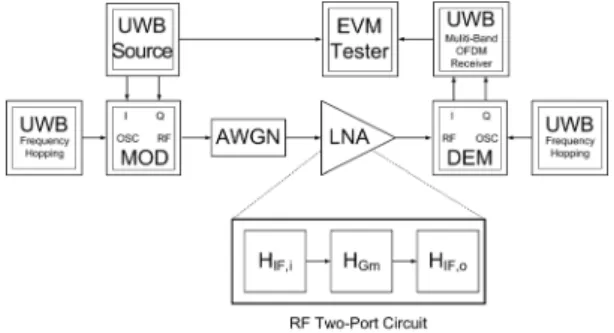
Fig. 1. UWB system simulation block diagram
II. UNIFIEDBEHAVIORALMODEL FORRF CIRCUITS
Here, we focus on the RF building blocks of two-port network, such as amplifiers and filters. Mixers and switches are, on the other hand, beyond the scope of this paper. As shown in Fig. 1, the proposed behavior model consists of three modules: input interface module (HIF,i) for the input impedance network, core module (HGm) for the gain stage, and output interface module (HIF,o) for the output load impedance. In a LTI system, the transfer function of the two-port network is represented by HIF,i · HGm · HIF,o in the system simulation platform. Detailed modeling approach for each module is described in the following sections.
A. Modeling of Input and Output Interfaces
The input/output impedance networks of a two-port circuit shape its frequency response and bandwidth. Though Laplace transfer function can be used to model the frequency re-sponse [3], it only defines the voltage/current transfer relation and requires additional impedance networks for the loading effect. The additional impedance networks nevertheless also shape the overall frequency response and introduce iterations in modeling. Instead of using Laplace transfer function, the proposed model employs equivalent impedance networks to portray the frequency response and the impedance matching properties of input/output interfaces at the same time.
An equivalent circuit consisting of resistors, inductors, and capacitors is established to model the input matching network and the input impedance of the active device. The capacitors and inductors are used to define the reactance ofHIF,i, while the resistors to define the loss including the resistor loss as well as the inductor loss and the capacitor loss. Physically,
139
Proceedings of the 9th European Conference on Wireless Technology
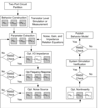
Fig. 2. Unified behavioral modeling flow
regular resistors contribute not only loss but also thermal noise. However, the equivalent resistors in HIF,i are not the actual thermal noise sources, and are intended to model the loss only. Similarly, the load impedance and the output impedance of the active device are modeled as a network of noiseless resistors, inductors, and capacitors.
B. Modeling of Gain Stage
The gain stage can be simply modeled by a controlled signal source, depending on the input and output signal types of the active devices. For example, voltage-controlled current sources (VCCS) and current-controlled current sources (CCCS) are used for common-source and common-emitter amplifiers, respectively. Since the impedance of the controlled signal sources have been considered in the interface modules, the controlled signal source in HGm is ideal and defines the input and output voltage/current relation either linear or nonlinear.
C. Modeling of Noise
The noise effects are lumped into an equivalent noise source instead of a noisy resistor as [3]. Hence the RF effects are modeled incrementally with iteration reduced. The noise effects of a two-port network are modeled by three equivalent noise sourcesin,IF,i,in,Gm andin,IF,ofor the input interface, core and output interface modules, respectively. For easy extraction of noise and model consistency,in,IF,i,in,Gm and
in,IF,o are all placed at the output node of each module. The
explicit input noise source of the active device, for example, is absorbed toin,IF,i in the preceding module.
Fig. 3. The target UWB LNA circuit
D. Modeling Flow
A modeling flow is developed for the proposed unified RF behavior model as depicted in Fig. 2. The two-port circuit is mapped into three behavior modules as mentioned above with RF characteristics relation equations in each module derived. This is a process of abstracting the physical circuit topology into a simplified equivalent circuit and grouping the equivalent circuit elements into each module accord-ingly, which has a great influence on the iterations in later optimization processes. From the results of the transistor-level simulation or measurement, the initial values for the model parameters in HIF,i, HGm and HIF,o are extracted. The parameter extraction is followed by four optimization processes to fit the model parameters for RF characteristics of input and output impedance, frequency response, noise and nonlinear effects in sequence. The optimization is a complex task due to the correlation among the RF characteristics, and therefore proceeded incrementally by considering the noise and nonlinear effects. That is, for small input signal condition, the two-port circuit is regarded as a noiseless linear circuit in the first two optimization procedures and then a noisy linear circuit in the noise optimization. On the other hand, the circuit is considered as a noisy weak-nonlinear network in the final optimization procedure. For reverse isolation concern, more iteration is required in the non-unilateral cases. The optimal model parameters are obtained if the root mean square error (RMSE) is smaller than a threshold value. Ultimately, a system simulation should be performed to verify the fidelity and feasibility of the RF behavior model.
III. MODELINGEXAMPLE OF ANUWB LNA In this section, a behavior modeling example of a CMOS LNA for ultra-wideband wireless applications is presented according to the above modeling procedure.
A. Construction of Equivalent Behavior Model
The targeting UWB LNA was fabricated in 0.18-μm CMOS technology and the circuit schematic is illustrated in Fig. 3. The LNA employs stagger tuning technique, which consists of two stacked common-source stages with different resonance frequencies [4]. The output buffer in Fig. 3 is for measurement
Fig. 4. The UWB LNA Model
Fig. 5. Comparison of input impedance.
purpose only and omitted in the behavior model. The behavior model of the UWB LNA contains three interface modules,
HIF,i,HIF,c andHIF,o, and two Gm-core modules,HGm,1 and HGm,2, mapping the two amplification stages as shown in Fig. 4.
B. I/O Interface
A simple RLC parallel network can be used to model the interface modules for narrow band circuits. To model the input band-pass matching network and the input impedance of transistor M1 of the UWB LNA, ideal lump elements
L1, L2, L3, C1, C2, C3 andR1 are used in HIF,i. HIF,c and HIF,o add RC4, RL4, RC5, and RL5 in the RLC parallel
network due to the low-Q loads of the wide-band amplifier. It should be noted again that all resistors framed in Fig. 4 are noiseless.
C. GmCore
In an N-stage amplifier, N numbers of Gm-core modules are exploited regardless its topology. The partition of the RF behavior model is determined by the critical impedance com-ponents which contribute the poles or zeros in the frequency response of the RF circuits. Two Gm coresGm,1 andGm,2, as a consequence, exist in the behavior model and their initial values are extracted from the small-signal transconductance values of transistors M1 and M2. Combining HGm,1 and
HGm,2withHIF,i,HIF,c, andHIF,o, the frequency response is optimized to portray the noiseless linear characteristic of the UWB LNA.
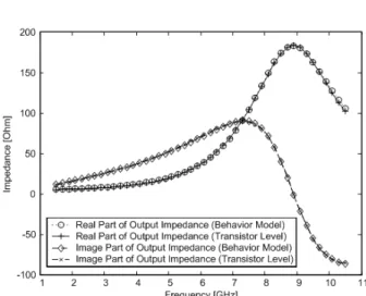
Fig. 6. Comparison of output impedance.
D. Noise Sources
The noise sources considered in the RF behavior model are only thermal noise contributed by the resistors and transistors of the RF amplifier while the flicker noise of MOSFET devices is not critical. The thermal noise of a MOSFET device includes gate noise and drain current noise [5]. For calculation simplicity, the drain current noise source stays in theGm-core module and the gate noise source is, on the contrary, placed in the preceding interface module. The noise of HIF,c and
HIF,o is also merged into the preceding Gm-core modules.
Consequently, three noise sourcesin1,in2andin3are adopted to describe the noise performance.
E. Nonlinearity
The UWB LNA is assumed weakly nonlinear and then modeled with Taylor series for its transfer function [6]. In addition, the nonlinear effect is dominated in the second stage of the UWB LNA. Therefore, the nonlinearity is simply related to the third order coefficient (α3) of Taylor series in HGm,2 and its initial value is set to be α3= 43 Av
A2
IIP 3.
IV. COMPARISON OFTRANSISTOR-LEVELCIRCUIT AND
BEHAVIORMODEL
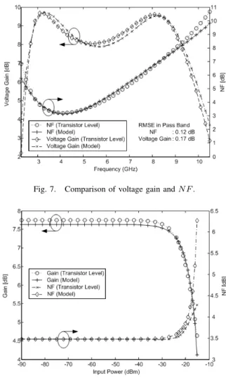
The simulation results of input/output impedance, noise figure, voltage gain, input 1-dB compression point and IP3 of the RF behavior model agree well with those of the transistor-level UWB LNA as shown in Fig. 5–9.
Fig. 7. Comparison of voltage gain andNF .
Fig. 8. Comparison of NF and power gain with sweeping RF power.
Error vector magnitude (EVM) simulation based on multi-band OFDM UWB design library in Agilent ADS platform is performed to validate the unified RF behavior model. With the circuit envelope simulator, the platform allows co-simulating of baseband algorithms and RF Verilog-A models. The input signal is 480-Mbps OFDM modulated at 5.016 GHz with power level sweeping from −72.8 to −27.8 dBm. The simulation results shown in Fig. 10 agree well with those of the transistor-level LNA with EVM RMS error less than 0.79% and the simulation time for all power sweeps is reduced 87%. The simulation results verifies the accuracy of the unified RF behavior model and demonstrates great efficiency.
V. CONCLUSION
An RF behavior model has been presented to predict RF effects of noise, impedance mismatch, frequency response, and nonlinear distortion of two-port RF circuits for system simu-lation. The proposed modeling approach allows modeling the RF effects incrementally with iteration reduced. The accuracy of the model is verified with both RF simulations and system EVM simulation. The model provides convincing prediction capability and great efficiency in system simulation compared with transistor-level circuit.
Fig. 9. Comparison of input IP3 and 1-dB compression point in the frequency band of interest.
Fig. 10. Comparison of UWB system EVM simulation results.
ACKNOWLEDGEMENT
This work was supported jointly by the National Science Council and Ministry of Economic Affairs of Taiwan, under the contract NSC94-2220-E-009-013 and 94-EC-17-A-01-S1-048, respectively. The authors would like to thank Agilent Technologies for the support of system simulation platform.
REFERENCES
[1] M. Jeruchim, P. Balaban, K. Shanmugan, “Simulation of Communication Systems,” Plenum Press, New York, 1992.
[2] F. Verbeyst and M.V. Bossche. “VIOMAP, the S-Parameter Equivalent for Weakly Nonlinear RF and Microwave Devices,” International Microwave Symposium Digest 94.3, pp. 1369–1372, 1994.
[3] W. Yang, H. Cater and J. Yan, “A high-level VHDL-AMS model design methodology for analog RF LNA and mixer,” Proc. Behavioral Modeling and Simulation Conference, pp. 125–129, October 2004.
[4] Mei-Fen Chou, Wen-Shen Wuen, Chang-Ching Wu, Kuei-Ann Wen, and Chun-Yen Chang, “A CMOS Low-Noise Amplifier for Ultra Wideband Wireless Applications,” in IEICE Trans. Fundamentals, vol. E88-A, No. 11, pp. 3110–3117, November 2005.
[5] A. van der Ziel, “Thermal Noise in Field Effect Transistors,” in Proc.
IEEE, August 1962, pp. 1801–1812.
[6] Willy Sansen, “Distortion in elementary transistor circuits,” in Proc.
IEEE, vol. 46, No. 3, pp. 315–325, March 1999.