www.pss-rapid.com
pss
Improved high-temperature switching
characteristics of Y
2O
3/TiO
xresistive
memory through carrier depletion effect
Zhi-Wei Zheng1
, Hsiao-Hsuan Hsu2
, Chun-Hu Cheng*, 3
, and Po-Chun Chen4 1 Institute of Microelectronics, Chinese Academy of Sciences, Beijing 100029, P.R. China 2 Department of Electronics Engineering, National Chiao Tung University, Hsinchu 30010, Taiwan 3 Department of Mechatronic Technology, National Taiwan Normal University, Taipei 10610, Taiwan 4 Department of Engineering and System Science, National Tsing Hua University, Hsinchu 30013, Taiwan
Received 22 January 2014, revised 20 March 2014, accepted 9 April 2014 Published online 22 April 2014
Keywords resistive random access memories, Y2O3, TiOy, carrier depletion, resisitive switching
* Corresponding author: e-mail [email protected], Phone: +886 2 7734 3526, Fax: +886 2 2358 3074
© 2014 WILEY-VCH Verlag GmbH & Co. KGaA, Weinheim
1 Introduction Since the technology node scales down with the continuous trend of nonvolatile memory (NVM) toward high density, fast speed and low power consumption, the conventional flash memory [1–3] has approached technical and physical limitations. Recently, non-charge based resistive random access memory (RRAM) [4–21] has attracted much attention as one of the most promising candidates in the next-generation NVM application, due to its simple structure, low cost, high switching speed, low power consumption and high com-patibility with the complementary metal–oxide–semi-conductor (CMOS) processes. However, due to the barrier height lowering at high temperature, the apparent degrada-tion on sneak current and current distribudegrada-tion are major challenges, especially for the scaled one-diode–one-resistor (1D1R) RRAM crossbar arrays. Therefore, the RRAM devices with excellent high-temperature switching characteristics are of great importance for production. Here, from our experimental results, we found that the
conven-tional filament conduction mechanism might suffer from high-temperature leakage issues including large switching current, wide current distribution and high sneak current. The sneak current in resistive crossbar memory is an inher-ent disadvantage and urginher-ently needs to be solved.
There-fore, we proposed a Y2O3/TiOx RRAM device, showing
good high-temperature switching characteristics of the self-compliance function, an extremely low reset power of ~1 μW at 150 °C, good current distribution at 85 °C and large rectification ratio of ~300 at 150 °C. The improve-ment in high-temperature performance is mainly ascribed
to the adoption of stacked Y2O3/TiOx and the unique
car-rier depletion effect in TiOx during switching. The present
results show high potential for future high-performance memory application.
2 Experimental procedure The proposed Ni/Y2O3/
TiOx/TaN RRAM devices with metal–insulator–metal
(MIM) structure were fabricated as follows. First, 100 nm We report a stacked Y2O3/TiOx resistive random access
mem-ory (RRAM) device, showing good high-temperature switch-ing characteristics of extremely low reset current of 1 μA at 150 °C, large off/on resistance window (>200) at 150 °C, large rectification ratio of ~300 at 150 °C and good current distribution at 85 °C. The good rectifying property, lower high-temperature sneak current and tighter high-temperature current distribution can be attributed to the combined results of the oxygen vacancies in TiOx and the related carrier deple-tion effect.
thick TaN was prepared by sputtering as the bottom gate
on the SiO2/Si substrate. After that, 15 nm thick TiOx and
8 nm thick Y2O3 films were deposited using e-gun
evapo-ration. Finally, 50 nm thick Ni was formed and patterned as the top electrodes, which provides high work function (5.1 eV) and works as a low-cost solution for high-κ DRAM capacitors [22]. The fabricated devices were char-acterized by current–voltage (I–V), capacitance–voltage (C–V), cycled endurance and X-ray photoelectron spec-troscopy (XPS) measurements. To precisely analyze film bonding, the film samples were pretreated by using in-situ Ar bombardment for 10 s at a low vacuum base pressure of
8 × 10⁻⁸ torr to remove the native oxide on the sample
sur-face.
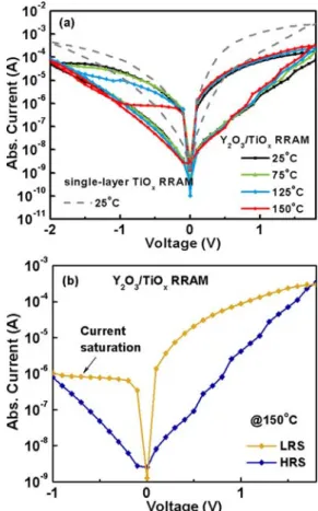
3 Results and discussion Figure 1(a) shows the swept I–V characteristic of the RRAM devices with a
sin-gle-layer TiOx and Y2O3/TiOx, respectively, which both
show counterclockwise bipolar switching behaviors. The asymmetric I–V curves are attributed to the different work-functions between top Ni and bottom TaN electrodes. It is clearly to observe that the set and reset currents are large
for single-layer TiOx RRAM device. However, the
switch-ing currents can be further improved after large bandgap
Y2O3 capping. The large bandgap Y2O3 dielectric owns
large conduction band offset that can form a large barrier
Figure 1 (a) Temperature-dependent I–V characteristics and (b) swept I–V curve at 150 °C of Y2O3/TiOx RRAM device.
height with TiOx to lower high-resistance state (HRS) and
low-resistance state (LRS) currents. In addition, the form-ing-free and self-compliance functions for set/reset cur-rents are also observed, which can simplify the array op-erations. No electroforming process is required for the
Y2O3/TiOx RRAM device. This forming-free property
could be attributed to the abundant oxygen vacancies
pre-existing in the TiOx, which forms a low-voltage conductive
path during the first switching from HRS to LRS. Thus, in
comparison with single-layer TiOx RRAM, the stacked
Y2O3/TiOx RRAM exhibits a larger resistance memory
window of ~50 at a reading voltage of 0.5 V and lower set and reset powers. The temperature dependence of the I–V characteristics was also measured as shown in Fig. 1(a). In the reset process, a decreasing current trend (positive tem-perature coefficient; TC) is apparently observed from 25 °C to 150 °C in LRS. The positive TC indicates that the current transport in LRS is mainly governed by filament
conduction. The filamentary switching in the TiOx via Ti
interstitial ions has been proposed in metal-oxide RRAM [16]. Furthermore, it is worthy to note that the reset current can reach a saturated current of 1 μA (current saturation), as shown in Fig. 1(b), which is unique and different to conventional filamentary RRAM. From the right I–V plot measured at 150 °C, we observe that the high-temperature I–V curve in HRS is similar to that of DRAM capacitor with MIM structure, which is dominated by asymmetric electrodes and less affected by bulk vacancies. However, the I–V curve in LRS shows the rectified properties of MIS (metal–insulator–semiconductor) or MS (metal–semicon-ductor) structures, suggesting that the LRS current at high temperature of 150 °C is not only determined by metal filament, but also related to interface junction leakage in this dielectric stack.
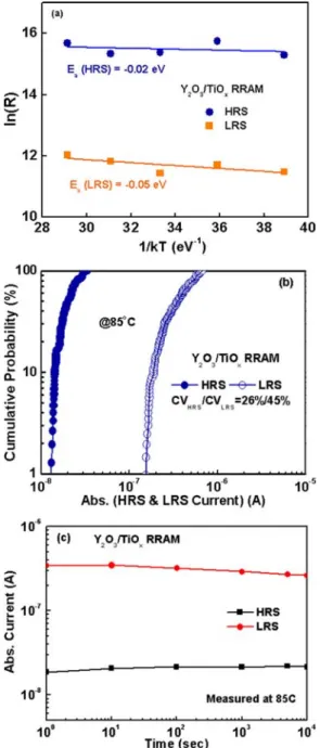
To explain the operation mechanism at high
tempera-ture, Fig. 2(a) displays the calculated active energy (Ea)
for Y2O3/TiOx RRAM device according to the HRS and
LRS resistances at different temperatures (from 25 °C to 125 °C), which are obtained at 0.5 V read under 1.8 V set/ –2 V reset operations. The extracted results reveal negative
Ea values for the device (Ea(HRS) = –0.02 eV, Ea(LRS) =
–0.05 eV), which implies that the conduction behaviors
are metallic (positive TC) in TiOx [23, 24]. Although the
Ni/Y2O3/TaN device has no RRAM memory property, this
metallic behaviour has been confirmed in Ni/TiOx/TaN
de-vice. The amorphous TiOx with incomplete bonding is
ex-pressed by the following equation: Ti–Ox* → VTi O2 x
+
- + 2e–
+ Ti–Ox, where VTi O2 x
+
- indicates the oxygen vacancies in
TiOx that dominate the resistive switching characteristics.
To further test the feasibility of the Y2O3/TiOx RRAM
at high temperature, we measured the HRS/LRS current distributions at 85 °C, as shown in Fig. 2(b). The current distribution measurements were performed under 60 μs pulses at 1.8 V set/–2 V reset voltages for 100 cycles. Here, the CV is an index of probability distribution, defined as the ratio of the standard deviation and mean value. Good current distribution for HRS (26%) and LRS (45%) was
Figure 2 (a) Extracted Ea at HRS and LRS conditions under
dif-ferent temperatures (from 25 °C to 125 °C), (b) current distribu-tions at 85 °C, and (c) 85 °C retention property for Y2O3/TiOx
RRAM device.
measured for the devices, indicating that the number of filament paths affects the switching distribution of RRAM. As shown in Fig. 2(c), the small current decays in HRS and
LRS were measured for 104 s retention at 85 °C. Thus, the
stable high-temperature performances are related to the low LRS current switching for less stress via defective films.
Figure 3(a) depicts the forward-to-reverse (FR) current ratio under 1.8 V set/–2 V reset operations, which is essen-tial for achieving a high memory density in crossbar arrays. A FR ratio of ~300 for the devices is measured at 150 °C.
Figure 3 (a) Forward-to-reverse ratios for Y2O3/TiOx RRAM de-vice; inset: formation of the depletion layer. (b) Temperature-dependent C–V characteristics for Y2O3/TiOx device; inset: sche-matic plot of the reset process.
The well rectified characteristic in LRS can effectively alleviate the sneak current in crossbar memory arrays, es-pecially at high-temperature operation. The rectified be-havior is believed to be related to depletion effect in n-type
TiOx with narrow bandgap. This is because a large number
of thermally excited electrons are generated in n-type TiOx
with increasing the measured temperature from 25 °C to 150 °C. The resulting excess electrons would lower the
intrinsic resistance of n-type TiOx and localize interface
electric field to form a depletion layer in TiOx, as shown in
the inset of Fig. 3(a). The carrier depletion phenomenon can be confirmed by C–V measurements, as reported in Refs. [25, 26]. Figure 3(b) shows the
temperature-dependent C–V characteristics for our Y2O3/TiOx device,
with the schematic band diagram under reset process in the inset. It is observed that the capacitance decreases with increasing temperature under the reset process using negative bias. The reduction in capacitance with tempera-ture up to 150 °C can be regarded as a capacitance-series effect. The temperature-dependent C–V characteristics in-dicate that the variation in capacitance with temperature directly corresponds to the change of depletion region in
electron-rich n-type TiOx, which is also supported by
the temperature dependence of the reduced reset current in Fig. 1(a).
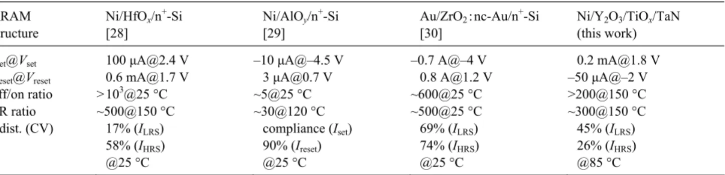
Table 1 Comparison of device integrity data for RRAM devices with rectified characteristic. RRAM structure >Ni/HfOx/n+-Si >[28] >Ni/AlOy/n+-Si >[29]
>Au/ZrO2:nc-Au/n+-Si
>[30]
>Ni/Y2O3/TiOx/TaN >(this work)
Iset@Vset >100 μ[email protected] V –10 μA@–4.5 V –0.7 A@–4 V >0.2 [email protected] V
Ireset@Vreset >0.6 [email protected] V >3 μ[email protected] V >0.8 [email protected] V –50 μA@–2 V
off/on ratio >103@25 °C ~5@25 °C ~600@25 °C >200@150 °C FR ratio ~500@150 °C ~30@120 °C ~500@25 °C ~300@150 °C I dist. (CV) >17% (ILRS) >58% (IHRS) >@25 °C >compliance (Iset) >90% (Ireset) >@25 °C >69% (ILRS) >74% (IHRS) >@25 °C >45% (ILRS) >26% (IHRS) >@85 °C In Fig. 4(a), the in-situ XPS result corresponds to
the oxidation state of Y3+ (156.8 eV and 158.9 eV), which
agrees with stoichiometric Y2O3 [27]. The well-oxidized
Y2O3 as capping layer is helpful to enhance the interface
barrier height between Y2O3 and TiOx that is critical for
lowering the switching power and unwanted sneak current.
Figure 4(b) shows the Ti 2p XPS spectra in the TiOx.
Dif-ferent Ti ion chemical states are measured in the TiOx
di-electrics. The low-valence Ti atoms with lower binding
en-ergy such as Ti3+ and Ti2+ confirm more oxygen vacancies
in the TiOx dielectric, which provide metallic filaments and
high electron carrier density under high-temperature opera-tion.
Figure 4 (a) In-situ XPS spectra of Y 3d core level for Y2O3
di-electric. (b) XPS spectra of Ti 2p core levels for TiOx dielectric.
Table 1 shows the comparison of resistive switching characteristics for various RRAM devices with rectified characteristics. It is well known that the sneak current and low FR ratio at high temperature are a major problem due to temperature-induced barrier height lowering. With the
combination of oxygen vacancies in TiOx and the related
carrier depletion effect, a large off/on resistance window (>200) at 150 °C, large rectification ratio of ~300 at 150 °C and good current distribution at 85 °C are all reached in our device. More importantly, the CV of high-temperature current distribution at 85 °C is even compara-ble to those of others measured at 25 °C.
4 Conclusion We reported a Ni/Y2O3/TiOx/TaN RRAM with good high-temperature characteristics. The
Y2O3/TiOx device can reach a large off/on resistance
win-dow (>200), a large FR ratio of ~300 and a low reset cur-rent of 1 μA (reset power ~1 μW) at a high temperature of 150 °C. Such good high-temperature switching
characteris-tics can be explained by the oxygen vacancies in TiOx and
related carrier depletion effect. This is beneficial to im-prove the high-temperature sneak current in recent 1D1R crossbar arrays and has great promise for future memory application.
Acknowledgements This work was supported by the
Na-tional Science Council (NSC) of Taiwan, Republic of China, un-der contract No. NSC 102-2221-E-003 -019.
References
[1] J. D. Lee, S. H. Hur, and J. D. Choi, IEEE Electron Device Lett. 23, 264 (2002).
[2] C. Y. Tsai, T. H. Lee, A. Chin, H. Wang, C. H. Cheng, and F. S. Yeh, Tech. Dig. – Int. Electron Devices Meet. 2010, 110.
[3] C. Zhu, Z. Xu, Z. Huo, R. Yang, Z. Zheng, Y. Cui, J. Liu, Y. Wang, D. Shi, G. Zhang, F. Li, and M. Liu, Appl. Phys. Lett. 99, 223504 (2011).
[4] Z. Fang, H. Y. Yu, W. J. Liu, Z. R. Wang, X. A. Tran, B. Gao, and J. F. Kang, IEEE Electron Device Lett. 31, 476 (2010).
[5] W. Y. Chang, K. J. Cheng, J. M. Tsai, H. J. Chen, F. Chen, M. J. Tsai, and T. B. Wu, Appl. Phys. Lett. 95, 042104 (2009).
[6] C. Chen, Y. C. Yang, F. Zeng, and F. Pan, Appl. Phys. Lett.
97, 083502 (2010).
[7] Q. Liu, J. Sun, H. Lv, S. Long, K. Yin, N. Wan, Y. Li, L. Sun, and M. Liu, Adv. Mater. 24, 1844 (2012).
[8] M. J. Lee, C. B. Lee, D. Lee, S. R. Lee, M. Chang, J. H. Hur, Y. B. Kim, C. J. Kim, D. H. Seo, S. Seo, U. I. Chung, I. K. Yoo, and K. Kim, Nature Mater. 10, 625 (2011). [9] L. Zhang, R. Huang, M. Zhu, S. Qin, Y. Kuang, D. Gao,
C. Shi, and Y. Wang, IEEE Electron Device Lett. 31, 966 (2010).
[10] A. Sawa, T. Fujii, M. Kawasaki, and Y. Tokura, Appl. Phys. Lett. 88, 232112 (2006).
[11] M. Wang, H. Lv, Q. Liu, Y. Li, Z. Xu, S. Long, H. Xie, K. Zhang, X. Liu, H. Sun, X. Yang, and M. Liu, IEEE Elec-tron Device Lett. 33, 1556 (2012).
[12] X. Sun, B. Sun, L. Liu, N. Xu, X. Liu, R. Han, J. Kang, G. Xiong, and T. P. Ma, IEEE Electron Device Lett. 30, 334 (2009).
[13] B. Gao, B. Sun, H. Zhang, L. Liu, X. Liu, R. Han, J. Kang, and B. Yu, IEEE Electron Device Lett. 30, 1326 (2009). [14] N. Xu, L. Liu, X. Sun, X. Liu, D. Han, Y. Wang, R. Han,
J. Kang, and B. Yu, Appl. Phys. Lett. 92, 232112 (2008). [15] C. Yoshida, K. Tsunoda, H. Noshiro, and Y. Sugiyama,
Appl. Phys. Lett. 91, 223510 (2007).
[16] U. Russo, D. Ielmini, C. Cagli, A. L. Lacaita, S. Spiga, C. Wiemer, M. Perego, and M. Fanciulli, Tech. Dig. – Int. Electron Devices Meet. 2007, 775.
[17] C. H. Cheng, A. Chin, and F. S. Yeh, IEEE Electron Device Lett. 31, 1020 (2010).
[18] C. H. Cheng, K. Y. Chou, A. Chin, and F. S. Yeh, Tech. Dig. – Int. Electron Devices Meet. 2010, 512.
[19] C. H. Cheng, A. Chin, and F. S. Yeh, IEEE Electron Device Lett. 32, 366 (2011).
[20] C. H. Cheng, A. Chin, and F. S. Yeh, Adv. Mater. 23, 902 (2011).
[21] Z. W. Zheng, C. H. Cheng, K. I. Chou, M. Liu, and A. Chin, Appl. Phys. Lett. 101, 243507 (2012).
[22] K. C. Chiang, C. H. Cheng, H. C. Pan, C. N. Hsiao, C. P. Chou, A. Chin, and H. L. Hwang, IEEE Electron Device Lett. 28, 235 (2007).
[23] C. H. Cheng, and A. Chin, Appl. Phys. Express 6, 041203 (2013).
[24] D. H. Kwon, K. M. Kim, J. H. Jang, J. M. Jeon, M. H. Lee, G. H. Kim, X. S. Li, G. S. Park, B. Lee, S. Han, M. Kim, and C. S. Hwang, Nature Nanotechnol. 5, 148 (2010). [25] S. S. Iyer, P. M. Solomon, V. P. Kesan, A. A. Bright, J. L.
Freeouf, T. N. Nguyen, and A. C. Warren, IEEE Electron Device Lett. 12, 246 (1991).
[26] N. Maffei and S. B. Krupanidhi, J. Appl. Phys. 72, 3617 (1992).
[27] Y. Uwamino, Y. Ishizuka, and H. Yamatera, J. Electron Spectrosc. Relat. Phenom. 34, 67 (1984).
[28] X. A. Tran, B. Gao, J. F. Kang, X. Wu, L. Wu, Z. Fang, Z. R. Wang, K. L. Pey, Y. C. Yeo, A. Y. Du, M. Liu, B. Y. Nguyen, M. F. Li, and H. Y. Yu, Tech. Dig. – Int. Electron Devices Meet. 2011, 713.
[29] X. A. Tran, W. Zhu, W. J. Liu, Y. C. Yeo, B. Y. Nguyen, and H. Y. Yu, IEEE Electron Device Lett. 33, 1402 (2012). [30] Q. Zuo, S. Long, Q. Liu, S. Zhang, Q. Wang, Y. Li,