582 IEEE ELECTRON DEVICE LETTERS, VOL. 27, NO. 7, JULY 2006
High-Performance TFTs With Si Nanowire Channels
Enhanced by Metal-Induced Lateral Crystallization
C.-J. Su, H.-C. Lin, Senior Member, IEEE, and T.-Y. Huang, Fellow, IEEE
Abstract—Thin-film transistors with poly-Si nanowire (NW)
channels enhanced by metal-induced lateral crystallization (MILC) are reported. The new device features a side-gate with self-aligned NW channels abutting the sidewalls of the gate struc-ture. By adopting the MILC technique, the crystallinity of the NW channels is greatly enhanced, compared to those formed by solid-phase crystallization. As a result, the electrical performance of the devices could be significantly enhanced in terms of reduced subthreshold swing and threshold voltage as well as improved field-effect mobility.
Index Terms—Metal-induced lateral crystallization (MILC),
nanowires (NWs), thin-film transistors (TFTs).
I. INTRODUCTION
P
OLYCRYSTALLINE silicon (poly-Si) thin-film tran-sistors (TFT) are very attractive for applications to liquid-crystal display (LCD) drivers and three-dimensional electronics [1]. Several techniques, including excimer laser annealing (ELA) [2] and metal-induced lateral crystallization (MILC) [3], have been developed to form high-quality poly-Si layer with high carrier mobility, large grain size, and low de-fect density. Among these techniques, MILC seeded by nickel is particularly attractive for yielding superior poly-Si layers with good electrical characteristics that meet device application requirements.On the other hand, FETs with nanowire (NW) channels have recently drawn a lot of attention for a number of applications, such as NW TFTs [4], memory devices [5], and biosensors [6]. By taking advantage of the high surface-to-volume ratio inher-ent in the structure, NWs can provide high surface sensitivity for sensing device applications [6], [7]. The preparation of NWs could be categorized into two types, namely: 1) top-down [7], [8] and 2) bottom-up [5], [6]. However, there remain certain distressing issues for either approach. For example, the top-down methods usually require costly equipment and cutting edge techniques, whereas the bottom-up methods may suffer from the uncontrollability of structural parameters, such as the length and diameter of NWs. Precise positioning of the NWs represents another major obstacle for reliable device fabrication. These issues may hinder practical applications and manufacturing of NW devices. Recently, Lin et al. [9] have pro-posed a simple and inexpensive approach to implement TFTs
Manuscript received April 12, 2006. This work was supported in part by the National Science Council, Taiwan, R.O.C., under Contract NSC 94-2120-M-009-017. The review of this letter was arranged by Editor J. Sin.
The authors are with the Department of Electronics Engineering, National Chiao-Tung University, Hsinchu 300, Taiwan, R.O.C.
Digital Object Identifier 10.1109/LED.2006.877708
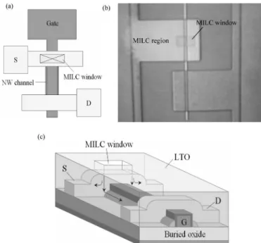
Fig. 1. (a) Top view of the layout, (b) optical microscopy image of MILC at 550◦C for 16 h, and (c) the schematic of poly-Si NW TFTs enhanced by MILC. The arrows indicate the MILC directions.
with poly-Si NW channels. The proposed structure overcomes all the major drawbacks previously mentioned. However, the new device was demonstrated on NWs formed by solid-phase crystallization (SPC) and was therefore susceptible to consid-erable grain boundaries and microstructural defects in the NW, which would unavoidably degrade device performance.
In this letter, we employ the MILC technique to the fab-rication of the novel NW devices to further improve device performance. Because the grains formed by MILC are large and could be deliberately formed parallel to the channel direction, it becomes feasible to form Si NWs with nearly monocrystalline structures [10]. The experimental results indeed reveal much improved performance over SPC devices.
II. DEVICEFABRICATION
Basically, the fabrication flow follows that described in the previous report [10], with the addition of the implementation of the MILC process. The top and side views of the device structure are depicted in Fig. 1(a) and (c), respectively. In addition, Fig. 1(b) shows an optical micrograph of a fabricated device. As shown, a window is opened in the oxide layer overlying the source region. Before the MILC treatment, a 5-nm-thick Ni layer was deposited in the window area to serve
SU et al.: HIGH-PERFORMANCE TFTs WITH Si NANOWIRE CHANNELS ENHANCED BY MILC 583
Fig. 2. Comparison of transfer characteristics between SPC and MILC TFTs with NW channels.
TABLE I
COMPARISONS OFDEVICEPARAMETERSBETWEENSPCANDMILC TFTS
as the seeding layer. Lateral crystallization was carried out at 550◦C for 16 h in an N2ambient, which also served the purpose of dopant activation. The unreacted Ni was then removed by an H2SO4/H2O2solution. As shown, the portion surrounding the window with different colors indicates the region that has been crystallized. For comparison, control samples that were crystallized by SPC at 600◦C for 24 h were also fabricated.
III. RESULTS ANDDISCUSSION
Transfer characteristics of SPC and MILC poly-Si TFTs with NW channels are compared in Fig. 2. The devices have a nominal channel length L of 1 µm and a channel width
W of 45 nm. The gate oxide is 40 nm thick. Detailed
de-vice characteristics are summarized in Table I. The field-effect mobility extracted from maximum transconductance is 201 cm2/V· s for the MILC device, which is much higher
than the 31 cm2/V· s of the SPC counterpart. In addition,
the MILC TFT has better subthreshold swing (SS, about 0.26 V/dec) and higher on/off current ratio (about 107). These results clearly indicate that NW channels formed by MILC are suitable for high-performance device applications. We believe this is because the grain is large, needlelike, and parallel to
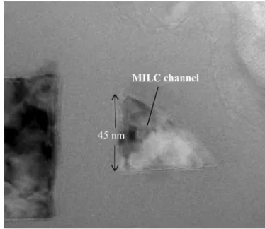
Fig. 3. TEM image of an MILC-crystallized transistor.
Fig. 4. Plot of ln(ID/VG) versus (1/VG) and the extracted effective trap
density of SPC and MILC TFTs. IDwas measured at VD= 0.5 V.
the channel for the MILC device. Fig. 3 shows the cross-sectional transmission electron microscopy (TEM) image of a fabricated device with MILC channels. As compared with the SPC sample characterized in our previous work [9], the film crystallinity is significantly improved, demonstrating the effectiveness of the MILC process in NW structures. When the size of the NW channel is shrunk to a dimension comparable to the grain size, a quasi-single-crystalline Si NW could be obtained [10].
Fig. 4 shows the trap densities (Nt) extracted from the slope
of ln(ID/VG) versus (1/VG) according to the grain-boundary
trap model [11], [12]. It can be found that the Nt of the
MILC TFT is about four times smaller than that of the SPC TFT. This result further confirms that the MILC technique results in much fewer grain boundaries and microstructural
584 IEEE ELECTRON DEVICE LETTERS, VOL. 27, NO. 7, JULY 2006
defects in the NW channel. It should also be noted that the MILC NW devices with high mobility and on/off ratio could provide favorable conductivity and switching characteristics suitable for high-sensitivity chemical and biological sensor applications.
Though the aforementioned enhancement in device perfor-mance is magnificent, the OFF-state leakage of the devices remains high despite the MILC treatment. This is likely to be due to potential Ni contamination. The formation of silicide at the grain boundaries during the MILC process has been reported previously [13], which would aggravate the leakage. This drawback could be alleviated by adoption of a long Ni-offset structure [14] or by proper annealing conditions [13]. Through further posttreatment (e.g., hydrogenation or high-temperature annealing), further improvement in electrical per-formance is expected.
IV. CONCLUSION
In summary, by adopting the MILC process to the newly proposed TFTs with Si NW channels, excellent device per-formance could be obtained. The fabricated devices exhibit large on current, high on/off ratio, low ss, and favorable output characteristics. The extracted effective trap density and mobil-ity further confirm that fewer defects and good crystallinmobil-ity in the NW channels are indeed achieved by MILC. The MILC-enhanced NW devices with good electrical characteristics and low-cost processes could be highly promising for future practi-cal manufacturing and applications.
ACKNOWLEDGMENT
The authors would like to thank H.-H. Tsai, C.-M. Huang, and the National Nano-Device Laboratories for their assis-tance in device fabrication. They would also like to thank Prof. Y.-S. Yang, C.-C. Lee, Dr. M.-C. Cheung, Dr. G.-R. Hu, C.-Y. Hou, and E. Wang for their valuable discussions and suggestions.
REFERENCES
[1] V. Subramanian, M. Toita, N. R. Ibrahim, S. J. Souri, and K. C. Saraswat, “Low-leakage germanium-seeded laterally-crystallized single-grain 100-nm TFT’s for vertical integration applications,” IEEE Electron
Device Lett., vol. 20, no. 7, pp. 341–343, Jul. 1999.
[2] I. H. Song, C. H. Kim, S. H. Kang, W. J. Nam, and M. K. Han, “A new multi-channel dual-gate poly-Si TFT employing excimer laser annealing recrystallization on pre-patterned a-Si thin film,” in IEDM Tech. Dig., Dec. 2002, pp. 561–564.
[3] S. W. Lee, T. H. Ihn, and S. K. Joo, “Fabrication of high-mobility p-channel poly-Si thin film transistors by self-aligned metal-induced lateral crystallization,” IEEE Electron Device Lett., vol. 17, no. 8, pp. 407–409, Aug. 1996.
[4] X. Duan, C. Niu, V. Sahi, J. Chen, J. W. Parce, S. Empedocles, and J. L. Goldma, “High-performance thin-film transistors using semiconduc-tor nanowires and nanoribbons,” Nature, vol. 425, no. 6955, pp. 274–278, Sep. 2003.
[5] X. Duan, Y. Huang, and C. M. Lieber, “Nonvolatile memory and program-mable logic from molecule-gated nanowires,” Nano Lett., vol. 2, no. 5, pp. 487–490, 2002.
[6] Y. Cui, Q. Wei, H. Park, and C. M. Lieber, “Nanowire nanosensors for highly sensitive and selective detection of biological and chemical species,” Science, vol. 293, no. 5533, pp. 1289–1292, Aug. 2001. [7] Z. Li, Y. Chen, X. Li, T. I. Kamins, K. Nauka, and R. S. Williams,
“Sequence-specific label-free DNA sensors based on silicon nanowires,”
Nano Lett., vol. 4, no. 2, pp. 245–247, 2004.
[8] F. L. Yang et al., “5 nm-gate nanowire FinFET,” in VLSI Symp. Tech. Dig., 2004, pp. 196–197.
[9] H. C. Lin, M. H. Lee, C. J. Su, T. Y. Huang, C. C. Lee, and Y. S. Yang, “A simple and low-cost method to fabricate TFTs with poly-Si nanowire channel,” IEEE Electron Device Lett., vol. 26, no. 9, pp. 643–645, Sep. 2005.
[10] J. Gu, S. Y. Chou, N. Yao, H. Zandbergen, and J. K. Farrer, “Single-crystal Si formed on amorphous substrate at low temperature by nanopatterning and nickel-induced lateral crystallization,” Appl. Phys. Lett., vol. 81, no. 6, pp. 1104–1106, Aug. 2002.
[11] J. Levinson, F. R. Shepherd, P. J. Scanlon, W. D. Westwood, G. Este, and M. Rider, “Conductivity behavior in polycrystalline semiconductor thin film transistors,” J. Appl. Phys., vol. 53, no. 2, pp. 1193–1202, Feb. 1982. [12] S. Seki, O. Kogure, and B. Tsujiyama, “A semi-empirical model for the field-effect mobility of hydrogenated polycrystalline-silicon MOSFET’s,”
IEEE Trans. Electron Devices, vol. 35, no. 5, pp. 669–674, May 1988.
[13] C. K. Chan, C. F. Cheng, and M. Chan, “Effects of dopants on the electri-cal behavior of grain boundary in metal-induced crystallized polysilicon film,” IEEE Trans. Electron Devices, vol. 52, no. 8, pp. 1917–1919, Aug. 2005.
[14] G. B. Kim, Y. G. Yoon, M. S. Kim, H. Jung, S. W. Lee, and S. K. Joo, “Electrical characteristics of MILC poly-Si TFTs with long Ni-offset structure,” IEEE Trans. Electron Devices, vol. 50, no. 12, pp. 2344–2347, Dec. 2003.