Investigation of Cu
ÕTaN Metal Gate for Metal-Oxide-Silicon
Devices
Bing-Yue Tsuizand Chih-Feng Huang
Department of Electronics Engineering and Institute of Electronics, National Chiao Tung University, Hsinchu, Taiwan
This work investigates the work function modulation of TaNxfilms and the thermal stability of Cu/TaNxstack as a gate electrode for metal-oxide-silicon devices. The N/Ta ratio was varied in the range of 0.30-0.65 by using reactive-sputter deposition with various Ar/N2 mass flow ratios. The TaNxfilms are almost amorphous and are thermally stable up to 800°C. However, the formation of Ta3N5 phase in a film with a high N/Ta ratio or annealed at high temperature increases the resistivity. The work function of TaNxis about 4.31-4.38 eV and the modulation is less than 70 mV. Such a short range modulation of the work function implies that TaNxis only suitable to be a gate electrode of surface channel n-channel metal oxide semiconductor field effect transistors共NMOSFETs兲. The mean value of the flatband voltage decreases and the deviation of the flatland voltage increases with the increase of the annealing temperature. Although phase change, grain growth, and Cu contamination contribute to the instability at high temperature, thermal stress-induced oxide charges dominate this decrease and deviation of the flatband voltage at tem-perature below 500°C. According to the material and electrical analysis, the Cu/TaNx stack gate electrode can be used for NMOSFETs only, and the maximum process temperature following gate electrode deposition should be lower than 500°C. © 2002 The Electrochemical Society. 关DOI: 10.1149/1.1522723兴 All rights reserved.
Manuscript submitted February 4, 2002; revised manuscript received June 13, 2002. Available electronically November 21, 2002.
As conventional complementary metal oxide semiconductor 共CMOS兲 devices are scaled down to improve performance, gate en-gineering becomes a crucial issue. It was found that the conven-tional gate material, poly-silicon, suffered from gate depletion, high gate resistance, and boron penetration into the channel region in sub-100 nm CMOS technology node.1-5Poly-Si gate depletion in-creases the equivalent gate dielectric thickness by about 3 Å and degrades channel current drive capability.1-3 High gate resistance increases the resistance/capacitance共RC兲 time delay to degrade high frequency performance. Salicide technology can reduce the gate re-sistance but it is difficult to maintain a proper aspect ratio for gate stack in scaled devices.4Boron penetration in p-channel metal oxide semiconductor field effect transistor共PMOSFET兲 reduces the ability of threshold voltage control and gate oxide reliability.1,5 High di-electric constant共high k兲 materials are expected to replace SiO2for scaling gate dielectric thickness below 1.5 nm where direct tunnel-ing current through SiO2may be too high to be acceptable.4 Unfor-tunately, poly-Si is incompatible with most high k materials due to chemical reaction or interface layer formation.6,7It has been dem-onstrated that metal gate devices are free from gate depletion, high resistance, and boron penetration. Therefore, there is an immense interest in metals to be a replacement in gate electrodes.
To select metal gate material properly, several issues must be considered to satisfy the manufacturability and performance. The typical thermal budget of front-end process usually causes thermal instability of metal gate devices. Therefore, low temperature or low thermal budget processes must be developed to prevent the metal gate from experiencing high temperature processes.8-11To simplify the process and to achieve high performance, the metal gate elec-trode should have low resistivity, suitable work function (⌽m), high thermodynamic stability, and good chemical durability under wet chemical processing. From these points of view, refractory metals such as W, Mo, Ta, and Ti are more attractive candidates. Since the work function of some refractory metal nitrides can be modulated with the nitrogen atom content, several investigations have been carried out in this field.12-14However, the nitrogen content also in-creases the resistivity of the metal. According to the ITRS roadmap of 2001, the effective resistivity of the gate electrode must be lower than 32⍀ cm.15This implies that several metal nitrides are not suitable to be used as a single layer gate electrode. Consequently, the gate electrode might be formed with stack structure that consists of a low resistivity metal and refractory metal nitride layers.12,16,17
Wherever it is possible, the low resistivity layer serves as the major conduction material and metal nitride layer serves as the threshold voltage control material.
Recently, the widely accepted barrier metal, TaNx, was reported as the gate electrode of fully depleted silicon-on-insulator devices and showed that its work function is closer to the midgap of silicon than that of-tantalum.17The Cu interconnect has become an alter-native to conventional Al interconnect, because of its low resistivity, low via resistance, and high electron-migration resistance.18 Inves-tigating the feasibility of using Cu/TaNx at the front-end-of-line
共FEOL兲, as the gate electrode, becomes natural.16 The use of Cu/TaNx at both the FEOL and back-end-of-line 共BEOL兲 can sim-plify the management of production line and reduce the cost-of-ownership because the equipment for BEOL can share with FEOL. Therefore, Cu/TaNx gate is one of the desirable gate structures. In
zE-mail: [email protected]
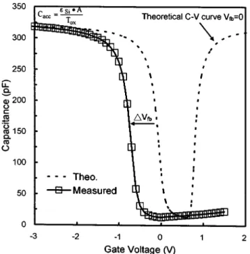
Figure 1. Example of the measured and the well-fitted theoretical capacitance/voltage curves for the extraction of corrected flatband voltage.
this work, the work function modulation of TaNxfilm and the ther-mal stability of Cu/TaNxMOS devices were investigated. The crite-ria and the optimum thermal process conditions for Cu/TaNx gate MOS devices were proposed.
Experimental
Simple metal oxide semiconductor共MOS兲 capacitors were fab-ricated with a single damascene process on p-type共100兲-oriented Si wafers. After cleaning, a 500 nm thick thermal oxide was thermally grown and a 1 m thick oxide was deposited in a high-density-plasma chemical vapor deposition 共HDPCVD兲 system. A conven-tional photo-lithography process was then used to define an active region with an area of 300⫻ 300 m. The oxide in the active re-gion was etched by a two-step共dry by wet兲 process to prevent Si surface from being damaged. Following preoxidation cleaning, a dry oxide, 10 nm thick, was thermally grown at 900°C as the gate di-electric. The purpose of using such a thick gate oxide is to isolate the gate electrode issues from the ultrathin oxide issues. TaNxfilms with various Ta/N ratios were reactively sputtered in a physical va-por deposition共PVD兲 system to a thickness of 50 nm, with various gas-flow ratios of Ar to N2. Before deposition, the process chamber was pumped down to 10⫺7 Torr. During deposition, neither bias nor heating was applied to the wafers, and the chamber pressure was kept at 10⫺4 Torr. It is known that the PVD process may introduce physical bombardment damage and radiation damage to the substrate.19,20 The physical bombardment damage can be reduced with lower deposition power and zero substrate bias. Therefore, the dc power and radio frequency共rf兲 power were set to 15 kW and 350 W, respectively. Radiation-induced oxide charges can be neutralized after a postdeposition annealing at 400°C. The Ar/N2gas flow ratio was set to 60/12, 60/20, and 60/28 for TaN-1, TaN-2, and TaN-3 films, respectively. A 200 nm thick Cu film was continuously depos-ited on TaNx films as a seed layer in another chamber of the same PVD system, without exposing to air. Then a 1 m thick elec-trochemically deposited copper film was deposited. Finally, the chemical mechanical polishing separated MOS capacitors and a 30 nm thick silicon nitride film were deposited to passivate the Cu surface. The completed structure is Si3N4 (30 nm)/Cu (500 nm)/TaNx (50 nm)/SiO2 (10 nm)/Si substrate. The thickness of dielectric layers were measured with the ellipsometry method and the thickness of metal layers were in-spected with cross-sectional scanning electron microscopy共SEM兲.
The element ratios of TaNx films were determined with the Ru-therford backscattering spectroscopy 共RBS兲 analysis. The phase transformation after annealing at different temperatures was identi-fied with Cu K␣ radiation wild angle X-ray diffraction 共XRD兲 spec-trum. A transmission electron microscope共TEM兲 was used to deter-mine grain size as well as phase formation. On the other hand, the sheet resistance (Rs) of blanket TaNx films was measured with a four-point probes system to monitor the thermal stability of various films. Secondary ion mass spectroscopy 共SIMS兲 depth profiling technique was used to elucidate the distribution of Cu atoms in the Cu/TaNx gate MOS capacitor.
In the electrical analysis, high frequency capacitance-voltage 共C-V兲 characteristic was measured at a frequency of 100 kHz. Low frequency共C-V兲 characteristic was measured with a ramp voltage method.21The oxide thickness (Tox) was calculated from the capaci-tance at strong accumulation mode (Cacc⫽ oxA/Tox). The sub-strate concentration can be obtained by fitting the measured C-V curve with the theoretical C-V curve at the depletion mode without concerning the interface state density (Dit). Because of the rela-tively thick gate oxide, classical MOS theory can be applied and the equations used to generate theoretical C-V curve can be found in any general textbook.22
By shifting the measured C-V curve to coincide with the theo-retical curve, the flatband voltage can be determined without the interference from the variation of gate oxide thickness and substrate concentration. Figure 1 shows an example of the measured 400°C annealed Cu/TaN-2 sample and the well-fitted C-V curves. The per-fect coincidence between the measured and theoretical C-V curves confirms that no PVD damages induced charges remain after 400°C annealing. After subtracting the work function of Si substrate, we obtain the corrected flatband voltage (VFB,c) which is equal to Figure 2. Wide angle XRD spectrums of共a兲 TaN-1, 共b兲 TaN-2, and 共c兲
⌽m⫺Qeff/Cox, where⌽mis the work function of gate electrode and Qeffis the effective oxide charges. In the case of thin oxide or low oxide charge, the VFB,cbecomes very close to⌽m.
The corrected flatband voltage of TaNxafter annealing at 400 and 500°C was extracted according to the above procedure. However, as the Dit can not be ignored, the fitting error becomes large. In this case, the flatband voltage was estimated from the flatband capacitance.22Finally, the interface state density (Dit) at the midgap was measured with the high-low frequency method.23
Result and Discussion
Thermal stability of TaNxfilms.—The N/Ta ratios of TaNxfilms determined with RBS analysis are 0.3, 0.5, and 0.65 for TaN-1, TaN-2, and TaN-3 films, respectively. The phases of TaNxare quite thermally stable. Figures 2a-c show the wide angle XRD spectra of TaN-1, TaN-2, and TaN-3 films after annealing at various tempera-tures. For the TaN-1 film, an extremely weak Ta2N共101兲 signal was detected after annealing at all temperatures. No significant phase change was observed with the increase of annealing temperature except that a weak Ta3N5 signal appeared after 800°C annealing. The small peak at 32.5° of the 500°C annealed TaN-1 film cannot be found in the data sheets of Si Ta, and TaNx. It might be attributed to exterior particles and is hard to be identified from the single peak.
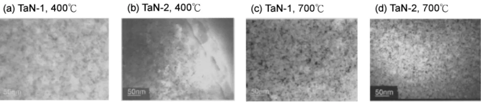
No XRD signal was detected for the TaN-2 film after annealing at different temperatures. For TaN-3 film, the Ta3N5共320兲 phase is observed after 400°C annealing and the signal intensity increases with the increase in the annealing temperature. Because the signal intensity of XRD is relatively weak, grain size and phases are iden-tified with plane view inspection and diffraction pattern of TEM, respectively. Figure 3 shows the plane view TEM micrographs of TaN-1 and TaN-2 films after annealing at 400 and 700°C. Since there is no apparent grain boundary but only some microcrystals, the films are almost amorphous. Despite 700°C annealing treatment, the
grain is small and the grain sizes are in the nanometer range. It is sure that TaNx film is dense and has no serious grain growth, but some microcrystals are precipitated. The transmitted electron dif-fraction patterns identify the phases of TaN-1 and TaN-2 more pre-cisely than those identified with XRD. As shown in Fig. 4, Ta2N and TaN phases were observed for TaN-1 and TaN-2 films, respectively, after annealing at 700°C.
The sheet resistance of TaNx films was also measured to under-stand the effect of phase transformation. The resistivities of the as-deposited TaN-1, TaN-2, and TaN-3 films were 463, 480, and 1290 ⍀ cm, respectively. Figure 5 shows the variation of sheet resis-tance of the three kinds of TaNx films vs. annealing temperature. These values were normalized to the sheet resistance of the corre-sponding films annealed at 400°C. A slight decrease of sheet resis-tance is observed in the TaN-1 and TaN-2 films upon increasing the annealing temperature form 400 to 700°C. Referring to the TEM pictures in Fig. 3, the decrease of sheet resistance is attributed to the slight grain growth with the increase of annealing temperature. Ac-cording to Radhakrishnan et al., the Ta3N5 phase has a very high resistivity.24Thus, the sheet resistance of TaN-1 film increased sud-denly at 800°C which can be attributed to the formation of Ta3N5 phase, as identified with the XRD spectra. Unlike TaN-1 and TaN-2 films, the sheet resistance of TaN-3 films increases with the anneal-ing temperature. The XRD spectra reveal that the increase is due to the growth of Ta3N5phase after high temperature annealing.
Flatband voltage variation of Cu/TaNx MOS capacitor.— Figure 6 shows the corrected flatband voltage (VFB,c) of Cu/TaN-1, Cu/TaN-2, and Cu/TaN-3 samples vs. the annealing temperature. All the VFB,cdifference of Cu/TaNxsamples is less than 70 mV below or at 600°C. This implies that the modulation of work function of TaNx film with the usage of various N/Ta ratios is very limited. In other words, the work function of TaNx film is quite stable against varia-tion induced by process disturbance. According to the ITRS
road-Figure 3. Plane view TEM micrographs of共a兲 TaN-1 film annealed at 400°C, 共b兲 TaN-1 film annealed at 700°C, 共c兲 TaN-2 film annealed at 400°C, and 共d兲
TaN-2 film annealed at 700°C.
Figure 4. Diffraction patterns of 共a兲
TaN-1 film annealed at 400°C,共b兲 TaN-1 film annealed at 700°C,共c兲 TaN-2 film annealed at 400°C, and共d兲 TaN-2 film annealed at 700°C.
map, the allowed deviation of threshold voltage (Vth) is 25 mV at the sub-0.07 m technology node.25For 400 °C annealing condi-tion, the 3-sigma共3兲 deviation of VFB,cof all samples satisfied the demand of 25 mV. Particularly, the 3 deviation of VFB,c of Cu/ TaN-2 sample is less than 5 eV. However, the deviation of VFB,c continuously increases with the increase of annealing temperature and is out of the demand after annealing at and beyond 500°C.
The reasons that cause the deviation of VFB,cinclude the charac-teristic of gate material, substrate doping concentration, oxide thick-ness, and oxide charges. The factors of oxide thickness and substrate deviation of 400 and 500°C annealed samples are ruled out using the Figure 5. Variation of sheet resistance of the three kinds of TaNxfilms vs.
annealing temperature.
Figure 6. Corrected flatband voltage (VFB,c) of共a兲 Cu/TaN-1 sample, 共b兲
Cu/TaN-2 sample, and共c兲 Cu/TaN-3 sample vs. the annealing temperature.
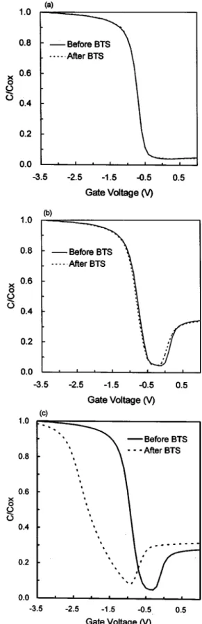
Figure 7. Capacitance/voltage curves before and after BTS test at ⫹1 MV/cm and 150°C for 60 min of Cu/TaN-2 sample annealing at共a兲 500°C,
VFB,cextracting procedure. The characteristics of gate electrode re-sulting in VFB,c variation are phase change and grain growth. The XRD spectra show no apparent difference among the TaNx films annealed below 700°C. The primary phase after annealing at 400°C changed from Ta2N to Ta3N5as the N/Ta ratio increased from 0.3 to 0.65 but the difference of VFB,cis only 70 mV. In addition, the VFB,c differences of Cu/TaNx samples annealed at the same temperature below 700°C are almost the same. It is thus clear that the phase transformation cannot dominate the VFB,cvariation. In other words, the main reason that caused the variation of VFB,c should be the variation of effectives oxide charges.
Copper contamination is the first possible factor to be examined. Figures 7a, b, and c show the C-V curves before and after bias-temperature stress共BTS兲 test at ⫹1 MV/cm and 150°C for 60 min of Cu/TaN-2 sample annealed at 500, 550, and 600°C, respectively. The C-V curves before and after BTS test of the 500°C annealed sample are identical. A slight shift of C-V curve toward the negative voltage axis after the BTS test is observed on the 550°C annealed sample. Furthermore, the appearance of a hump at the inversion region 共about ⫹0.5 V兲 reveals that the carrier lifetime at the Si substrate is shortened. Both the observations indicate that the device was contaminated, while the most possible contamination source is Cu.
The transient capacitance technique is sensitive to small quantity of deep-level atoms, such as copper.26,27 Once the copper reaches silicon, it affects the silicon/oxide interface and the minority carrier lifetime in the bulk. Therefore, transient capacitance analysis was performed to detect lifetime degradation. The MOS capacitor was
biased at the accumulation mode of⫺4 V and was switched to deep depletion mode of⫹5 V. The retention time is defined as the time required for capacitance to recover 90% of the stable value. Table I lists the retention time and its deviation of Cu/TaN-2 samples an-nealed at 400, 500, 550, and 600°C. The retention time of 550 and 600°C annealed samples decreases to shorter than 0.1 s, which in-dicates that copper had penetrated into the Si substrate. A slight decrease in the retention time of the 500°C annealed sample is dis-cussed later. Although SIMS was not detected Cu signal in the sub-strate of the 550°C annealed sample, Fig. 8 shows the SIMS depth profile of Cu in the 600°C annealed Cu/TaN-2 sample before BTS test. Before SIMS analysis, the Cu film was removed with dilute HNO3solution. It is thus concluded that the decrease of VFB,cand increase in the deviation of VFB,cbeyond 550°C annealing is related to Cu contamination. However, the decrease of VFB,cand increase of VFB,cdeviation occur after annealing at 500°C even if no Cu con-tamination would occur.
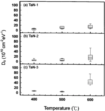
Figure 9 shows the interface state density (Dit) at the midgap of Cu/TaN-1, Cu/TaN-2, and Cu/TaN-3 samples vs. the annealing tem-perature. The magnitude and deviation of Ditincrease with the in-crease of annealing temperature. It is reasonable to expect that the effective oxide charges (Qeff) also increase with the increase of an-nealing temperature. A deviation in Qeffof 1⫻ 10
11
cm⫺2results in a deviation in flatband voltage of 46 mV. Therefore, VFB,cdeviation can be reasonably attributed to the deviation of Qeffinduced by the deviation of thermal stress. For 500°C annealed samples, the drop in the VFB,ccompared to the corresponding 400°C annealed samples is less than 60 mV, and the 3 deviation is about 50 mV which is higher than the value of the demand. It is postulated that the devia-tion of VFB,ccomes from the large difference of thermal expansion coefficient 共TEC兲 between Cu and Si. By scaling down the gate dielectric thickness, the effect of Qeffon threshold voltage can also be scaled down. However, the Qeffgenerated by thermal stress may increase. The slight increase in the retention time of 500°C annealed sample, listed in Table I, is thus explained by the increase of surface generation rate due to the increase of Dit. Replacing Cu by another low resistivity material with TEC close to Si, for example, W and Mo, is recommended.
Figure 8. SIMS depth profile of Cu of the 600°C annealed Cu/TaN-2 sample. No BTS was performed before SIMS analysis and the Cu layer was removed with dilute HNO3solution.
Figure 9. Interface state density (Dit) of共a兲 Cu/TaN-1 sample, 共b兲 Cu/TaN-2
sample, and共c兲 Cu/TaN-3 sample vs. the annealing temperature. Table I. Mean value and standard deviation of retention time of
CuÕTaN-2 MOS capacitors under transient capacitance measure-ment. Temperature 共°C兲 400 500 550 600 Retention time 共s兲 33.4 14.1 ⬍0.1 ⬍0.1 Deviation 共s兲 16.2 7.4 0 0
Above 600°C annealing, the VFB,crises with the annealing tem-perature. It is presumable that the interface dipoles caused by the interaction between oxide and metal gate induce effective work function offsets since effective oxide charges are increasing.28The interaction between metal gate and gate dielectric is still under in-vestigation.
Conclusion
This work investigates the work function modulation of TaNx film and the thermal stability of Cu/TaNxstack as the gate electrode. The N/Ta ratio was varied in the range 0.3-0.65 by using the reactive sputtering with various Ar/N2 gas flow ratios. The main phases of the TaN-1, TaN-2, and TaN-3 films are Ta2N, TaN, and Ta3N5, respectively. The TaNxfilms are thermally stable up to 800°C. How-ever, the formation of the Ta3N5 phase in a TaNx film annealed at high temperature or with a high N/Ta ratio increases the effective resistivity. The work function of TaNxis about 4.31-4.38 eV and the range is less than 70 mV. Such a short range work function modu-lation implies that the work function of TaNxfilm is quite stable to avoid the variation induced by process disturbance. On the other hand, TaNx is a suitable to be a gate electrode only for the surface channel n-channel metal oxide semiconductor field effect transistor 共NMOSFETs兲. The flatband voltage decreases with an increase in the annealing temperature. In addition, the deviation of the flatband voltage increases with the annealing temperature. Although phase change, grain growth, and Cu contamination contribute at high tem-perature, thermal stress-induced oxide charges dominate the de-crease and deviation of the flatband voltage at temperature below 500°C.
In conclusion, according to the material and electrical analysis, the Cu/TaNx stack can be used as a gate electrode for the surface channel NMOSFETs only, and the maximum process temperature following gate electrode deposition should be lower than 500°C. The thermal stress-induced oxide charges are additional sources of deviation in the threshold voltage. This result must be considered in controlling the threshold voltage during metal gate generation.
Acknowledgment
This work is partly supported by the National Science Council, ROC, under contract no. NSC89-2215-E-009-106.
National Chiao Tung University assisted in meeting the publication costs of this article.
References
1. B. Yu, D. H. Ju, N. Kepler, T. J. King, and C. Hu, in Technical Digest for VLSI Symposium, p. 105共1997兲.
2. K. Chen, M. Chan, P. K. Ko, C. Hu, and J. H. Huang, Solid-State Electron., 38, 1975共1995兲.
3. N. D. Arora, R. Rios, and C. L. Huang, IEEE Trans. Electron Devices, ED-42, 935
共1995兲.
4. The International Technology Roadmap for Semiconductors, p. 123, Semiconduc-tor Industry Association, San Jose, CA共1999兲.
5. J. R. Pfiester, F. K. Baker, T. C. Mele, H. H. Tseng, P. J. Tobin, J. D. Hayden, J. W. Miller, C. D. Gunderson, and L. C. Parrillo, IEEE Trans. Electron Devices, ED-37, 1842共1990兲.
6. H. F. Luan, B. Z. Wu, L. G. Kang, R. Vrtis, D. Roberts, and D. L. Kwong, Tech. Dig. - Int. Electron Devices Meet., 1998, 609.
7. C. H. Lee, H. F. Luan, W. P. Bai, S. J. Lee, Y. Senzaki, D. Roberts, and D. L. Kwing, Tech. Dig. - Int. Electron Devices Meet., 2000, 27.
8. A. Yagishita, T. Saito, K. Nakajima, S. Inumiya, Y. Akasaka, Y. Ozawa, G. Mi-namihaba, H. Yano, K. Hieda, K. Suguro, T. Arikado, and K. Okumura, Tech. Dig. - Int. Electron Devices Meet., 1998, 785.
9. H. Shimada, Y. Hirano, T. Ushiki, K. Ino, and T. Ohmi, IEEE Trans. Electron Devices, ED-44, 1903共1997兲.
10. Y. C. Yeo, Q. Lu, P. Ranade, H. Takeuchi, K. J. Yang, I. Polishchuk, T. J. King, C. Hu, S. C. Song, H. F. Luan, and D. L. Kwong, IEEE Electron Device Lett.,
EDL-22, 227共2001兲.
11. W. Saitoh, A. Itoh, S. Yamagami, and M. Asada, Jpn. J. Appl. Phys., Part 1, 38, 6226共1999兲.
12. H. Wakabayashi, Y. Saito, K. Takeuchi, T. Mogami, and T. Kunio, Tech. Dig. - Int. Electron Devices Meet., 1999, 253.
13. Q. Lu, R. Ronald, P. Ranade, T. J. King, and C. Hu, in Technical Digest for VLSI Symposium, p. 45共2001兲.
14. Y. S. Suh, G. Heuss, H. Zhong, S. N. Hong, and V. Misra, in Technical Digest for VLSI Symposium, p. 47共2001兲.
15. International Technology Roadmap for Semiconductors-Front End Process, p. 20, Semiconductor Industry Association, San Jose共2001兲.
16. T. Matsuki, K. Kishimoto, K. Fujii, N. Itoh, K. Yoshida, K. Ohto, S. Yamasaki, T. Shinmura, and N. Kasai, Tech. Dig. - Int. Electron Devices Meet., 1999, 261. 17. H. Shimada, I. Ohshima, T. Ushiki, S. Sugawa, and T. Ohmi, IEEE Trans. Electron
Devices, ED-48, 1619共2001兲.
18. S. Venkatesan, A. V. Gelatos, V. Misra, B. Smith, R. Islam, J. Cope, B. Wilson, D. Tuttle, R. Cardwell, S. Anderson, M. Angyal, R. Bajaj, C. Capasso, P. Crabtree, S. Das, J. Farkas, S. Filipiak, B. Fiordalice, M. Freeman, P. V. Gilbert, M. Herrick, A. Jain, H. Kawasaki, C. King, J. Klein, T. Lii, K. Reid, T. Saaranen, C. Simpson, T. Sparks, P. Tsui, R. Venkatraman, D. Watts, E. J. Weitzman, R. Woodruff, I. Yang, N. Bhat, G. Hamilton, and Y. Yu, Tech. Dig. - Int. Electron Devices Meet., 1997, 769.
19. K. Nakajima, Y. Akasaka, M. Kaneko, M. Tamaoki, Y. Yamada, T. Shimizu, and K. Suguro, in Technical Digest for VLSI Symposium, p. 95共1999兲.
20. B. Y. Tsui, S. H. Liu, G. L. Lin, J. H. Ho, and C. H. Chang, in Proceedings of the Symposium on Plasma Process-Induced Damage, American Vacuum Society, p. 148, May 13-14, 1996.
21. L. Sadwick, J. Electron. Mater., 19, 637共1990兲.
22. S. Sze, Physics of Semiconductor Devices, p. 368, John Wiley & Sons Inc., New York共1981兲.
23. E. H. Nicollian and J. R. Brews, MOS Physics and Technology, p. 331, John Wiley & Sons Inc., New York共1982兲.
24. K. Radhakrishnan, N. G. Ing, and R. Gopalakrishnan, Mater. Sci. Eng., B, 57, 224
共1998兲.
25. International Technology Roadmap for Semiconductors-Process Integration, De-vices, & Structures, p. 42, Semiconductor Industry Association, San Jose, CA 共2000兲.
26. C. N. Berlung, IEEE Trans. Electron Devices, ED-13, 701共1966兲.
27. Y. Shacham-Diamand, B. Israel, and Y. Sverdlov, Microelectron. Eng., 55, 13
共2001兲.