國 立 交 通 大 學
電 子 物 理 研 究 所
碩士論文
改善電洞傳導行為緩解Ⅲ族氮化物發光二極體效率
下降特性之研究
Efficiency droop alleviation in Ⅲ-nitride light-emitting diodes
by improving hole transportation
研究生:張瑋婷
指導教授:郭浩中 教授
林烜輝 教授
改善電洞傳導行為緩解Ⅲ族氮化物發光二極體效率下降特性之研究
Efficiency droop alleviation in Ⅲ-nitride light-emitting diodes by improving
hole transportation
研 究 生:張瑋婷 Student:Wei-Ting Chang
指導教授:郭浩中 教授 Advisor:Prof. Hao-Chung Kuo
林烜輝 教授 Prof. Shiuan-Huei Lin
國 立 交 通 大 學
電 子 物 理 系
碩 士 論 文
A Thesis
Submitted to Department of Electrophysics
College of Science
National Chiao Tung University
in Partial Fulfillment of the Requirements
for the Degree of Master
in
Electrophysics
March 2011
Hsinchu, Taiwan, Republic of China
改善電洞傳導行為緩解Ⅲ族氮化物發光二極體效率下降特性之研究
研究生:張瑋婷 指導教授: 郭浩中教授 林烜輝教授 國立交通大學電子物理系碩士班摘要
本論文中,我們針對為傳統氮化銦鎵發光二極體的磊晶結構進行改良,改善電洞 傳導行為以緩解三族氮化物發光二極體效率隨外加電流提高而驟降之問題。 第一部分設計漸變鋁含量的氮化鋁鎵電子阻擋層,期待除了強化阻檔電子溢流外, 更可增加電洞注入效率,藉以提升主動層載子複合發光效率,在以理論分析找得最佳 化設計後,實作樣品利用電激發螢光(Electroluminescence, EL)量測,驗證其發光強度 確實相較於使用傳統電子阻擋層之元件為佳,並且緩解了發光效率在高電流會產生效 率驟降的情況。 再者,我們在使用氮化銦鎵作為主動層量子井的紫外光(UV) LED 中,將位能障 材料氮化鋁鎵替換成氮化鋁鎵銦,量測證實其與三元材料晶格常數和能隙相近的四元 材料,有較好的磊晶品質外,EL 量測結果也顯示其突出的電特性與發光效率。由於四 元材料可以經由調整鋁和銦的含量而自由變動其晶格常數、能隙、應力、和載子侷限 效果,因此在藉由理論模擬分析後,我們推論使用氮化鋁鎵銦作為位能障,可以提高 量子井中電子的侷限、電洞的傳導與載子的遷移率,因而改善 LED 效率驟降的問題。Efficiency droop alleviation in Ⅲ-nitride light-emitting diodes by improving
hole transportation
Student : Wei-Ting Chang Advisor: Prof. Hao-Chung Kuo Prof. Shiuan-Huei Lin
Department of Electrophysics National Chiao Tung University
Abstract
In this thesis, we designed the epitaxial structure of InGaN light-emitting diodes (LEDs) to improve the transportation of holes, which leads to reduction of efficiency droop.
We first degined a graded-composition electron blocking layer (GEBL) for c-plane InGaN/GaN LEDs. The simulation results demonstrated that such GEBL can effectively enhance the capability of hole transportation across the EBL as well as the electron confinement. Consequently, the LED with GEBL grown by metal-organic chemical vapor deposition exhibited lower forward voltage and series resistance, and much higher output power at high current density, as compared to conventional LED.
Second, we demonstrated InGaN-based UV LEDs with AlGaN and InAlGaN barrier. EL results indicate that the light output performance could be enhanced effectively when replacing the conventional AlGaN barriers by InAlGaN barriers. Furthermore, from numerical analysis, it is believed that InGaN/AlInGaN MQWs exhibit higher radiative recombination rate and low efficiency droop at a high injection current because of the better band-offset ratio and the higher hole mobility, which leads to the uniform distribution of holes in the active region.
誌謝
很難相信兩年研究生涯會過得如此的快,直到現在還是覺得要畢業了很不真實。 想想這段時間裡過得非常充實,除了學術上知識的吸收外,也在實驗室中交到了許多 好朋友,使我有個多姿多采的碩班生活。在此,要感謝在這兩年中幫助、陪伴我成長 的人,使我可以順利完成我的碩士學位。 首先,我要感謝林烜輝老師和郭浩中老師的指導,謝謝老師提供了很好的研究環 境,還有平時對我的幫助與鼓勵,使我能夠有許多想法去解決研究上所遇到的問題。 感謝在我初進實驗室,帶著我學習的清華學長、閔安學長、小柯學長、與永吉學 長,使我熟習到理論知識與實驗技術,紮根了我 LED 研究的基礎。再來要感謝的是 Joseph 學長的照顧,對於我研究上的規劃幫助許多,除了 Meeting 上的指導,平常總 是不厭其煩的替我解答與給予建言,使我得以順利完成碩班研究。感謝李博學長、金 釵學姐、與鏡學學長,對於我在報告時提供不少想法與建議,令我收穫良多。感謝士 邦學長與涂學長,有你們的幫助我才能得到穩定的樣品完成研究。感謝總是很可靠的 小昕學長,不管是實驗與研究上的教導,還是私下的鼓勵與叮嚀,使我能有所成長。 感謝羿蓁、大寶、Jolin、肉圓、幼慶、小杜、家齊、阿 po、祐國、Just、SGG、等碩 二的同學們,因為有你們使我的碩班生活增添不少快樂回憶,我會永遠記得那些揪團 吃飯或是出遊的時光,一起分享歡笑與宣洩壓力,很開心可以認識到可愛的大家。感 謝 Bush 學弟,量測變溫 EL 有你協助輕鬆許多,能有你這麼聰明、負責的學弟真的很 幸運,也祝福你能在未來一年的順利完成研究、順利畢業。 最後要感謝我最最親愛的家人,感謝爸媽一直以來對我的支持與關愛,使我可以 安心的完成學業,謝謝你們!Content
摘要...i Abstract...ii 誌謝...iii Content...iv List of Tables...vi List of Figures...vii Chapter 1 Introduction 1.1 Bandgaps of group Ⅲ-nitride materials……….……...11.2 InGaN-based Light-Emitting Diodes (LEDs)……….……...2
1.3 Motivation………...4
Chapter 2 Properties of Ⅲ-Nitride semiconductor 2.1 Theory of radiative recombination and LED efficiency………...6
2.2 The basic concept of efficiency droop …...9
2.3 The mismatch of the charge carrier in Ⅲ-nitride LEDs…...11
2.4 The pros and cons of inserting electron blocking layer (EBL) in Ⅲ-nitride LEDs……..13
Chapter 3 Experimental instrument and numerical simulation 3.1 Electroluminescence (EL) measurement...15
3.2 Physical models and parameter setting...16
Chapter 4 Study of InGaN LEDs with graded-composition EBL 4.1 Introduction…...26
4.3 Calculated band diagrams and carrier distribution analysis...30
4.4 Sample structure and Fabrication…...35
4.5 Analysis of current-dependence EL characteristics and efficiency droop behavior...37
4.6 Summary…...39
Chapter 5 Study of InGaN-Based UV LEDs with InAlGaN Barrier 5.1 Introduction…... 41
5.2 Sample structure and fabrication…...43
5.3 Investigation of optical property and surface morphology…...45
5.4 Current-dependent intensity and efficiency...47
5.5 Theoretical analysis…...50
5.6 Summary…...55
Chapter 6 Conclusion...56
List of Tables
Table 3.1 Material parameters of the binary semiconductors GaN, AlN, and InN at room temperature……….……....19 Table 3.2 Bandgap energy of GaN, AlN and InN related-temperature parameters….…..21 Table 3.3 Mobility parameters of GaN, AlN and InN………...25 Table 5.1 Simulation parameters in band-offset ratio and carrier mobility………...53
List of Figures
Figure 1.1 Bandgap energy versus lattice constant of III-V nitride semiconductors at room temperature………1 Figure 1.2 The schematic drawing of InGaN LED……….……….3 Figure 2.1.1 Illustration of radiative and non-radiative transition in a semiconductor…..6 Figure 2.2.1 Efficiency droop of LEDs……….10 Figure 2.3.1 Carrier transportation and recombination behavior in MQWs………12 Figure 2.4.1 Calculated band diagrams of InGaN/GaN LEDs with Al0.32Ga0.68N EBL at
90 A/cm2……….….14
Figure 2.4.2 IQE and leakage current ratio of GaInN/GaN and GaInN/AlGaInN LEDs with and without polarization effect in the MQW and/or the EBL……….14 Figure 3.1.1 The schematic of electroluminescence setup……….…..15 Figure 3.1.2 The photograph of electroluminescence measure system………16 Figure 4.1 (a) The influence of inserting EBL between MQWs and p-GaN
(b)Schematic diagram of the concept of band engineering at EBL…….…27 Figure 4.2.1 The simulation structure of GEBL LEDs with material, thickness, and
doping concentration……….…29 Figure 4.2.2 The simulation structure of conventional LED, LED A, B, and C...29 Figure 4.3.1 Calculated energy band diagrams of (a) Al0GaN to Al0.15Ga0.85N,(b) Al0GaN
to Al0.25Ga0.75N, and (c) Al0GaN to Al0.35Ga0.65N graded-composition EBLs
at a current density of 100 A/cm2………..30 Figure 4.3.2 The calculated band diagram of GEBL LEDs at 20, 100, and 300 A/cm2…31 Figure 4.3.3 Simulated electron current density for conventional LEDs and GEBL
LEDs………..33 Figure 4.3.4 Distribution of hole concentration of conventional LEDs and GEBL
LEDs………..33 Figure 4.3.5 Calculated (a)hole concentration distribution and (b)electron concentration
distribution of conventional and GEBL LEDs at a current density of 100
Figure 4.4.1 The schematic drawing of sample structure (GEBL LED)……….…..36 Figure 4.4.2 The schematic drawing of fabrication processes of LED……….…36 Figure 4.5.1 Forward voltage and output power as a function of current density for
conventional and GEBL LEDs……….………….…38 Figure 4.5.2 Normalized efficiency as a function of current density for conventional and
GEBL LEDs……….……….….39 Figure 5.1.1 Calculated band diagram of reference GaInN/GaN LED as well as AlGaInN
LED structure with polarization-matched MQW under a forward bias
condition………42 Figure 5.1.2 Normalized EQE as a function of forward current density for
GaInN/AlGaInN MQW LEDs and reference GaInN/GaN MQW LEDs…..43 Figure 5.2 The schematic drawing of sample structure (UV LED)………....44 Figure 5.3.1 Room-temperature PL spectra of AlGaN and InAlGaN bulks. Insert Figs.
shows surface morphology AFM over 5×5 μm2 of bulk AlGaN (RMS:0.813 nm) and InAlGaN (RMS:0.595 nm) layer with thickness about 50 nm…...46 Figure 5.3.2 (a)HRXRD (ω-2θ) curves in the (002) reflections of InGaN/AlGaN and
InGaN/InAlGaN MQW. Cross-sectional TEM images of (b) InGaN/AlGaN and (c) InGaN/InAlGaN MQW. The diffraction condition is g0002………47 Figure 5.4 (a) L-I-V curves of the LEDs with AlGaN (dash) and InAlGaN (solid)
barrier. (b) Normalized Efficiency curves of experimental. Insert in Fig. 5.4(a) shows the mesa-type UV chips………...……49 Figure 5.5.1 Simulation results of normalized IQE under different carrier mobility….…51 Figure 5.5.2 Simulation results of normalized IQE under different band offset ratio…...52 Figure 5.5.3 Normalized Efficiency curves of experimental and simulated………..54 Figure 5.5.4 Distribution of (a) Electron (b) Hole concentrations, and (c) Radiative
recombination rates concentrations of the LEDs with AlGaN and InAlGaN barrier under a high forward current density of 100 A/cm2……….….54
Chapter 1 Introduction
1.1 Bandgaps of group III-Nitride materials
In recent decades, the III-Nitrides materials (InN, GaN, and AlN related alloys) become
an interesting class of wide bandgap materials and play an important role in semiconductor
devices. The bandgap of the wurtzite polytypes of III-nitrides material cover a very wide
range, from 0.7 eV for InN to 6.1 eV for AlN, which represents the emission wavelength from
infrared (IR) region to deep ultraviolet (UV). Fig. 1.1 shows the bandgaps of various alloys of
III-Nitrides.
Fig. 1.1 Bandgap energy versus lattice constant of III-V nitride semiconductors at room temperature. [1]
This wide emission wavelength range makes it promising for applying in the applications
of optoelectronic devices. By using III-Nitride with different alloy compositions, we can get a
material with the desired bandgap. This phenomenon is quite different from other III-V
materials systems based on GaAs, AlAs, InAs, GaP and related alloys. In addition, the
III-Nitrides materials are expected to be superior to the counterparts made of Si and other
III-V materials for high-temperature and high-power applications [2-5].
1.2 GaN-based LEDs
Light Emitting Diodes (LEDs) are solid state devices which emit light when electrical
current passes through them. In LEDs made of semiconductors, the color of the light depends
on the bandgap of the semiconductor material, proceeding from red through orange, yellow,
green, blue and violet as the gap increases.
The first blue light-emitting diode (LED) using III-Nitrides materials was fabricated by J.
I. Pankove et al. [6] with an metal-i-n structure in 1972. Since that, related research is going
on continually. However, progresses have been limited because of highly background n-type
concentration resulting from the native defects commonly thought to be nitrogen vacancies
and residual impurities such as Si and oxygen acted as an efficient donor, poorly conducting
p-type GaN, and the lack of appropriate substrates for epitaxial growth. Until late 1980s, H.
developed low-energy electron beam interaction (LEEBI) techniques to obtain better GaN
epilayer and conductive p-type GaN, initiated a new strong interest in this research field.
Finally, the first GaN-based blue LED constructed of a real p-n junction was achieved, which
had greatly improved in the device performance. However, the acceptor concentration of
p-type GaN is still too low such that the application of these materials is still unreliable. After
that, in 1992, S. Nakamura et al. [9] achieved better conductive p-type GaN material by
introducing a simple thermal annealing procedure in nitrogen ambient (≧ 750 ℃). Afterward
Nakamura and Mukai [10] succeeded in growing high-quality InGaN films that emitted strong
band-to-band emission from green to UV by changing the indium content of InGaN with a
two-flow MOCVD method. Nowadays, Most of III-Nitride based light emitting devices uses
InGaN as active layer instead of GaN because the difficulty of fabricating high efficiency
GaN based light emitting devices. Adding a small amount of indium into the GaN is very
important to obtain a strong band-to-band emission at RT. The based design of GaN LEDs is
shown in Fig. 1.2.
1.3 Motivation
Solid-state lighting offers much potential to save energy and enhance the quality of our
building environments, especially refers to GaN-based LEDs. However, for the high efficiency
lighting devices, III-nitride semiconductors have some inherent drawbacks to deteriorate the
lighting efficiency. This phenomenon which known as efficiency droop is a severe limitation for
high power devices that operate at high current densities and must be overcome to enable the
LEDs needed for solid-state general illumination. The efficiency droop is caused by a
nonradiative carrier loss mechanism, which is small at low currents but becomes significant for
high injection currents. Competition between radiative recombination and this droop-causing
mechanism results in the reduction in efficiency as current increases. The physical origin of
efficiency droop remains controversial, and several different mechanisms have been suggested as
explanations, including carrier leakage from the active region [11]. Auger recombination [12],
junction heating [13], and carrier delocalization from In-rich low-defect-density regions at high
carrier densities [14]. Carrier leakage in InGaN LEDs generally refers to the escape of electrons
from the active region to the p-type region. These leakage electrons may then recombine with
holes either in the p-type region or at the contacts, dominantly by nonradiative processes.
Therefore, fewer holes than electrons are injected into the active region. These two phenomena
that escape of electrons form the active region and reduced hole concentration of any carrier
possibly due to the low p-type doping efficiency or the electron blocking layer (EBL) acting as a
potential barrier also for holes. As a result of the low hole injection, current across the device is
dominated by electrons. Devices with p-type active regions which should increase hole injection
efficiency have been proposed as a solution to this problem.
For this thesis, we investigated the injection current dependence EL intensity at room
temperature. Then we discussed the normalized efficiency as a function of injection current
density at room temperature clearly and used APSYS simulation to make sure our model is correct,
so the physical mechanisms of current dependent efficiency of InGaN/GaN LED has been
confirmed.
This thesis is organized in the following way: In chapter 2, we give some theoretical
backgrounds and characteristics about InGaN MQW structures. The experimental setups and
theory model are stated in chapter 3. In chapter 4, we present the simulation and experiment
results and discuss for optical and electrical properties of InGaN/GaN MQW LED with graded
composition electron blocking layer. In chapter 5, we show the experiment results and discuss
for physical mechanisms of quaternary barrier MQW as a function of injection current density in
Chapter 2 Properties of Ⅲ-Nitride semiconductor
2.1 Theory of radiative recombination and LED efficiency
LEDs are a class of diode that emit spontaneous radiation under suitable forward
bias condition. Injection electroluminescence (EL) is most important mechanism for exiting
the semiconductor material. Under forward bias conditions, both electrons from n-type
semiconductor and holes from p-type semiconductor all inject to active region and then
recombine either ,and accompany by the emission of a photon (radiatively) or non-radiatively.
This two recombination pathways can be considered as parallel processes occurring across the
bandgap of the active region material, as illustrated in Fig. 2.1.1. If the radiative lifetime is
denoted as
τ
r and the non-radiative lifetime is denoted asτ
nr, then the total probability ofrecombination is given by the sum of the radiative and non-radiative probability:
nr r 1 1 1
τ
τ
τ
= + (2.1.1)Fig. 2.1.1 Illustration of radiative and non-radiative transition in a semiconductor.
over the total probability of recombination. Therefore, the internal quantum efficiency (IQE)
can be expressed in terms of the radiative and non-radiative lifetimes.
𝜂
int=
𝜏𝑟−1
𝜏𝑟−1+𝜏𝑛𝑟−1 (2.1.2) The IQE value of ideal active region of an LED is unity. From the concept of electrical
excitation mechanism, the internal quantum efficiency is defined as:
𝜂
int = number of photons emitted from active region per secondnumber of electrons injected into LED per second = 𝑃int𝐼/𝑒/ℎ𝜈 (2.1.3)where Pint is the optical power emitted from the active region and I is the injection current.
Photons emitted by the active region should escape from the LED die. In an ideal LED, all
photons emitted by the active region are also emitted into free space. Such an LED has unity
extraction efficiency. However, in a real LED, not all the power emitted from the active
region is emitted into free space. Some photons may never emit into the free space. This is
due to several possible loss mechanisms. For example, light may be reabsorbed by material
itself of the LED. Light may be incident on a metallic contact surface and be absorbed by the
metal. In addition, the phenomenon of the total internal reflection, also referred to as the
trapped light phenomenon, reduces the ability of light to escape from the active region.
The extraction efficiency can be a severe limitation for high performance LEDs. It is
sophisticated and costly device processes. The light extraction efficiency (LEE) is defined as:
𝜂
int = number of photons emitted from active region per secondnumber of photons emitted into free space per second = 𝑃𝑃/ℎ𝜈int/ℎ𝜈
(2.1.4)
where P is the optical power emitted into free space. Considering the refractive indices of
GaN (n = 2.5) and air, for the light escape cone, is about 23% due to the critical angle.
Assuming that light emitted from sidewalls and backside is neglected, one expects that
approximately only 4% of the internal light can be extracted from a surface.
The light outside the escape cone is reflected into the substrate and is repeatedly
reflected, then reabsorbed by active layers or electrodes, unless it escapes through the
sidewalls. However, there is much room for improvement of the light extraction efficiency.
For example, roughening of the top LED surface increased the light extraction efficiency.
Finally, the external quantum efficiency (EQE) is defined as:
𝜂
ext = number of photons emitted into free space per second number of electrons injected into LED per second =𝑃/ℎ𝜈 𝐼/𝑒
𝜂
ext =𝜂
int𝜂
extraction(2.1.5)
from the above equation, we can know that the EQE depend on IQE and LEE, therefore, the
improvement of IQE and LEE pay an important role of LED. Recently, the patterned
dislocation density and enhance the LEE due light emit to substrate may reflect and emit into
free space.
2.2 The basic concept of efficiency droop
Solid-state lightings, especially InGaN/GaN light-emitting diodes (LEDs), have been
vigorously developed to take the place of traditional lighting source, due to its potentially
higher efficiency. It is imperative that LEDs produce high luminous flux which necessitates
high efficiency at high current densities. However, as the efficiency of LEDs increasing, the
upcoming challenge is the efficiency “droop” for high-power applications [15]. The external
quantum efficiency EQE reaches its peak at current densities as low as 10 A/cm2 and monotonically decreases with further increase in current, as illustrated in Fig. 2.2.1. It means
Fig. 2.2.1 Efficiency droop of LEDs
Contrary to what may appear at an instant glance, dislocations have been shown to
reduce the overall efficiency but not affect the efficiency droop. The major cause of
efficiency droop is still a huge controversy. Various possible mechanisms of droop including
carrier overflow [16], non-uniform distribution of holes [17, 18], Auger scattering [19],
carrier delocalization [20], junction heating have been proposed, but the genesis of the
efficiency droop is still the topic of an active debate. Although Auger recombination was
proposed for the efficiency droop,[21]the Auger losses in such a wide bandgap
semiconductor are expected to be very small,[22] which has also been verified using fully
microscopic many body models.[23] In addition, if an inherent process such as Auger
undoubtedly prevented laser action, which requires high injection levels, in InGaN which is
not the case. The efficiency droop was also noted to be related to the quantum well thickness
in the form of peak efficiency shifting to higher injection currents with increasing well
thickness.[24] It was suggested that the effect of polarization field may be playing a role.[25]
The observations, however, are consistent with large effective mass of holes because of
which it is very likely that only the first QW next to the p-barrier substantially contributes to
radiative recombination. Making the well wider, therefore, increases the emission intensity
providing that the layer quality can be maintained. It has also been suggested that in wider
QWs the carrier density is reduced for the same injection level and thus reduced Auger
recombination.[25] What is very revealing is that in below barrier photoexcitation
experiments (photons absorbed only in the QWs), where carriers are excited and recombined
in the QWs only, the efficiency droop was not observed at carrier generation rates
comparable to electrical injection which indicates that efficiency droop is related to the
carrier injection, transport, and leakage processes.[25]
2.3 The mismatch of the charge carrier in III-nitride LEDs
The transportation behavior of electrons and holes in III-nitride are known to be
(near p-side layer) difficult. On the other hand, high electron concentrations are achievable
with the n-type dopant Si due to its relatively low ionization energy of about 20 meV,[26]
and electron mobility is fairly high, with values above 200 cm2 V−1 s−1 being typical for n-type GaN. By contrast, high hole concentrations are generally not achievable due to the
large ionization energy of the p-type dopant Mg in GaN, which has been estimated at 120
meV.[27] In addition, hole mobility is typically on the order of 10 cm2 V−1 s−1 for doped p-type GaN.[28] Furthermore, due to poor hole transport, the radiatively recombination
distribution in MQWs come to be non-uniform and gather in nearest p-side wells, as
illustrated in Fig. 2.3.1. Then, in high current injection, this mismatch of the charge carrier
could also produce electron overflow or auger recombination and be one of origins for
efficiency droop.
2.4 The pros and cons of inserting electron blocking layer in III-nitride LEDs
Carrier overflow out of the active region as well as inefficient injection and
transportation of holes have been identified to be the major reasons of efficiency droop.[18,
30] To reduce the carrier overflow, an AlxGa1−xN electron blocking layer (so called EBL)
was adopted in common InGaN LED structures. However, it has been reported that the large
polarization field in AlxGa1−xN EBL reduces the effective barrier height for electrons, as
shown in Fig. 2.4.1.[32] Therefore, the carrier overflow cannot be suppressed effectively. On
the other hand, the polarization-field induced band bending and the valence band offset (∆Ev)
at the interfaces of GaN and EBL are considered to retard the injection of holes.[31, 32] To
reduce the polarization field in EBL, the polarization-matched EBLs (AlInN or AlInGaN)
were proposed and demonstrated to be more effective in electron confinement.[33, 34]
However, it has difficulties of realization in epitaxy, and the crystal quality of the subsequent
p-GaN layer will be degraded. Most importantly, the hole injection cannot be improved
Fig 2.4.1 Calculated band diagrams of InGaN/GaN LEDs with Al0.32Ga0.68N EBL at 90
A/cm2 [32].
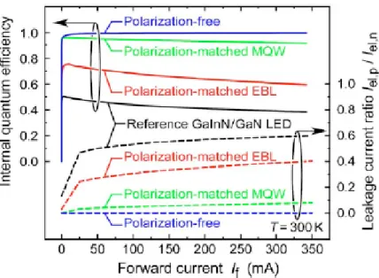
Fig 2.4.2 IQE and leakage current ratio of GaInN/GaN and GaInN/AlGaInN LEDs with and without polarization effect in the MQW and/or the EBL. [31]
Chapter 3 Experimental instrument and numerical simulation
3.1 Electroluminescence (EL)
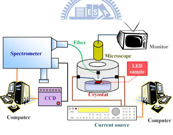
Fig. 3.1.1 shows the schematic of electroluminescence measurement systems. A set of
instruments including CW current source Kiethley 238, a microscope to observe the
patterned electrode of sample surface, three axial stages for probe and fiber to detected the
light output, and then the light detected by a 0.32 m monochromator (Jobin-Yvon Triax-320)
with 1800, 1200, and 300 grooves/mm grating and the maximum width if the entrance slit
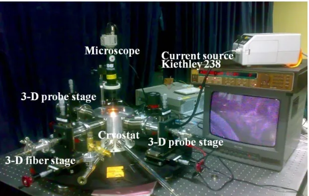
was 1 mm. Figure B shows the photograph of electroluminescence measure system.
Fig. 3.1.2 The photograph of electroluminescence measure system.
3.2 Physical models and parameter setting
To explore theoretically this study, the numerical simulation software, APSYS
(Advanced Physical Models of Semiconductor Devices), was used to preview and optimize
our LEDs design, and it is based on 2D/3D finite element analysis of electrical, optical and
thermal properties of compound semiconductor devices. Emphasis is placed on band
structure engineering and quantum mechanical effects. Inclusion of various optical modules
also makes this simulation package attractive for applications involving photosensitive or
light emitting devices. The APSYS simulator solves the Poisson’s equation, the current
and the heat transfer equations, via self-consistent manner. Built-in polarization induced by
spontaneous and piezoelectric polarization is considered at hetero-interfaces of nitride
related devices. We put commonly accepted physical parameters to perform the simulations.
Usually, for performing a simulation, the used material parameters had been set as default
data from former research results. However, we also can modify and update these values to
be similar to real device. Therefore, setting suitable parameters for simulation is an
important point.
3.2.1 Theoretical model
The physical model of the InGaN MQWs is considered in such a way that the
conduction bands are assumed to be decoupled from valence subbands and have isotropic
parabolic bands due to the larger bandgap of nitride semiconductor and the valence band
structures, which includes the coupling of the heavy-hole (HH), the light-hole (LH), and the
spin-orbit split-off bands, are calculated by the 6×6 Hamiltonian with envelop function
approximation. By using the basis transformation, the 6×6 Hamiltonian can be transformed
into a block-diagonalized Hamiltonian [35],
𝐻6×6 = �𝐻 𝑈 0 0 𝐻𝐿� with 𝐻𝑈 = � 𝐹 𝐾𝑡 −𝑖𝐻𝑡 𝐾𝑡 𝐺 Δ − 𝑖𝐻𝑡 𝑖𝐻 Δ + 𝑖𝐻 𝜆 � , 𝐻 𝐿 = � 𝐾𝐹𝑡 𝐾𝐺𝑡 Δ + 𝑖𝐻𝑖𝐻𝑡 𝑡 −𝑖𝐻 Δ − 𝑖𝐻 𝜆 �
𝐹 = Δ1+ Δ2 + λ + θ , 𝐺 = Δ1 − Δ2+ λ + θ λ = 2mℏ2 0�𝐴1𝑘z 2+ 𝐴 2𝑘t2� + λℇ , λℇ = 𝐷1ℇzz+ 𝐷1�ℇxx+ ℇyy� 𝐾t = ℏ 2 2m0𝐴5𝑘t 2 , 𝐻 t = ℏ 2 2m0𝐴6𝑘z𝑘t ∆= √2∆3 , and 𝑘t2 = 𝑘x2 + 𝑘y2
where m0 is the free electron mass. The Ai parameters are related to the hole effective
masses. The crystal-field split energy is Δcr = Δ1 and the spin-orbit splitting is Δso = 3Δ2 =
3Δ3. The Di parameters are deformation potential constants.
To obtain the numerical parameters required for calculations for the nitrogen-containing
semiconductors, a linear interpolation between the parameters of the relevant binary
semiconductors is utilized except for the unstrained bandgap energies. The material
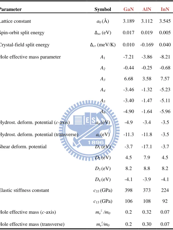
parameters of the binary semiconductors are taken from the paper by Vurgaftman and Meyer
Table 3.1 Material parameters of the binary semiconductors GaN, AlN, and InN at room temperature. ( ∆cr=∆1, ∆so=3∆2=3∆3 )
Parameter Symbol GaN AlN InN
Lattice constant a0 (Å) 3.189 3.112 3.545
Spin-orbit split energy ∆so (eV) 0.017 0.019 0.005
Crystal-field split energy ∆cr (meV/K) 0.010 -0.169 0.040
Hole effective mass parameter A1 -7.21 -3.86 -8.21
A2 -0.44 -0.25 -0.68
A3 6.68 3.58 7.57
A4 -3.46 -1.32 -5.23
A5 -3.40 -1.47 -5.11
A6 -4.90 -1.64 -5.96
Hydrost. deform. potential (c-axis) az (eV) -4.9 -3.4 -3.5
Hydrost. deform. potential (transverse) at (eV) -11.3 -11.8 -3.5
Shear deform. potential D1 (eV) -3.7 -17.1 -3.7
D2 (eV) 4.5 7.9 4.5
D3 (eV) 8.2 8.8 8.2
D4 (eV) -4.1 -3.9 -4.1
Elastic stiffness constant c33 (GPa) 398 373 224
c13 (GPa) 106 108 92
Hole effective mass (c-axis) mez /m0 0.2 0.32 0.07
3.2.2 Bandgap energy of Ⅲ-nitride Alloys
As being mentioned before, nitride-based materials are mainly made up of three binary
compounds (GaN, AlN, and InN), so the bandgap energy of these nitride-based compounds is
also made up of these binary materials. Besides, the bandgap energy of these three binary
materials is related to the temperature. Therefore, we will extend this discussion to ternary
and quaternary nitride-based compound in the next paragraph.
The bandgap energy of GaN, AlN, and InN at temperature T can be expressed by the
Varshni formula (3.2.1) [37]
𝐸g(𝑇) = 𝐸g(0) − 𝛼𝑇 2
𝑇 + β
where Eg(T) is the bandgap energy at temperature T, Eg(0) is the bandgap energy at 0 K, α and
β are material-related constant, of the binary alloys are listed in Table 3.2.[36]
The bandgap energy of InxGa1-xN and AlxGa1-xN ternary alloys measured by Osamura et
al. [38] at room temperature (RT) is treated as
𝐸g(In𝑥Ga1−𝑥N) = 𝑥 ∙ 𝐸g(InN) + (1 − 𝑥) ∙ 𝐸g(GaN) − bowing ∙ 𝑥 ∙ (1 − 𝑥)
𝐸g(Al𝑥Ga1−𝑥N) = 𝑥 ∙ 𝐸g(AlN) + (1 − 𝑥) ∙ 𝐸g(GaN) − bowing ∙ 𝑥 ∙ (1 − 𝑥)
𝐸g(Al𝑥In1−𝑥N) = 𝑥 ∙ 𝐸g(AlN) + (1 − 𝑥) ∙ 𝐸g(InN) − bowing ∙ 𝑥 ∙ (1 − 𝑥)
and the bandgap energy of AlxInyGazN quaternary alloy is [39]
𝐸g�Al𝑥InyGazN� =
𝑥𝑦 T12�1 − 𝑥 + 𝑦2 � + 𝑦𝑧 T23�1 − 𝑦 + 𝑧2 � + 𝑥𝑧 T13�1 − 𝑥 + 𝑧2 �
𝑥 ∙ 𝑦 + 𝑦 ∙ 𝑧 + 𝑧 ∙ 𝑥
Where “bowing” is the so-called bowing parameter (also called bowing vector), which is 7.0
eV for AlInN, 3.0 eV for InGaN, and 1.0 eV for AlGaN in our calculation, and the suffix 1, 2,
and 3 is taken for AlN, InN, and GaN, respectively.
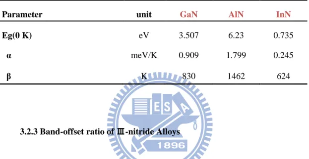
Table 3.2 Bandgap energy of GaN, AlN and InN related-temperature parameters
Parameter unit GaN AlN InN
Eg(0 K) eV 3.507 6.23 0.735
α meV/K 0.909 1.799 0.245
β K 830 1462 624
3.2.3 Band-offset ratio of Ⅲ-nitride Alloys
The value of band-offset, which plays a very important role in the analysis of energy
band diagram, is quite significant for the design of heterostructure devices. In some other
textbooks, band-offset is also called band discontinuity, and it is obvious that when two
different materials are grown next to each other, the conduction and the valence bands of the
two materials will become discontinuous at the interface. However, the devotion of the
determination of the band-offset values in semiconductor hetero-junction from experimental
measurements and theoretical calculations exists large discrepancy which may be related to
(B) Possible dependence of band discontinuity on detailed, conditions of interface
preparation,
(C) Strain dependence of band discontinuity.
And they may be related to the difficulty of obtaining high equality epitaxial films.
The conduction band offset ratio (∆E c/∆Eg) for the AlN/GaN interface is between 0.66
and 0.81 according to the recent calculations [40]. In our study, a band offset ratio of 67/33 for
the all interface is assumed principally.
3.2.4 Carrier transportaion of Ⅲ-nitride Alloys
The physical model of carrier transport is the traditional drift-diffusion model for
semiconductors. The specific equations can be expressed as
𝐽𝑛
���⃑ = q𝜇𝑛𝑛 𝐹⃑ + q𝐷𝑛∇𝑛 (for electrons)
and 𝐽���⃑ = q𝜇𝑝 𝑝𝑝 𝐹⃑ + q𝐷𝑝∇𝑝 (for holes)
where n and p are the electron and hole concentrations, 𝐽���⃑ and 𝐽𝑛 ���⃑ are the current densities of 𝑝 electrons and holes, 𝐹⃑ is the electrostatic field, 𝜇𝑛 and 𝜇𝑝 are the mobilities of electrons and
holes. The diffusion constants 𝐷𝑛 and 𝐷𝑝 are replaced by mobilities using the Einstein
relation 𝐷 = 𝜇𝑘𝐵𝑇/q. The equations used to describe the semiconductor device behavior are
∇ ∙ �ε0ε𝐹⃑� = q�𝑝 − 𝑛 + 𝑝𝐷 − 𝑛𝐴 ± 𝑁𝑓�
and the current continuity equations for electrons and holes,
1q ∇ ∙ 𝐽���⃑ − 𝑅𝑛 𝑛+ 𝐺𝑛 =𝜕𝑛𝜕𝑡 (for electrons)
1q ∇ ∙ 𝐽���⃑ − 𝑅𝑝 𝑝+ 𝐺𝑝 = 𝜕𝑝𝜕𝑡 (for holes)
where ε is the relative permittivity. 𝐺𝑛 and 𝑅𝑛 are the generation rates and recombination
rates for electrons, 𝐺𝑝 and 𝑅𝑝 are the generation rates and recombination rates for holes,
respectively. The electric field is affected by the charge distribution, including the electron
and hole concentrations, dopant ions 𝑝𝐷 and 𝑛𝐴, and other fixed charges 𝑁𝑓 that are of
special importance in nitride-based devices due to the effect of built-in polarization.
Built-in polarization induced due to spontaneous and piezoelectric polarization is known
to influence the performance of nitride devices. In order to consider the built-in polarization
within the interfaces of nitride devices, the method developed by Fiorentini et al. is employed
to estimate the built-in polarization, which is represented by fixed interface charges at each
hetero interface. They provided explicit rules to calculate the nonlinear polarization for nitride
alloys of arbitrary composition. [41]
Although the interface charges can be obtained by this theoretical model, experimental
investigations often find weaker built-in polarization than that predicted by theoretical
80% smaller than the theoretically calculated values. [43] As a result, 50% of the theoretical
polarization values are used in our simulation from the average of the reported values.
A widely used empirical expression for modeling the mobility of electrons and holes is
the Caughey Thomas approximation, which is employed in our calculation and can be
expressed as [44]
𝜇(𝑁) = 𝜇min+1 + (𝑁/𝑁𝜇max− 𝜇min ref)𝛼
where 𝜇max, 𝜇min, 𝑁ref and 𝛼 are fitting parameters. The parameter 𝜇max represents the
mobility of undoped or unintentionally doped samples, where lattice scattering is the main
scattering mechanism, while 𝜇min is the mobility in highly doped material, where impurity
scattering is dominant. The parameter 𝛼 is a measure of how quickly the mobility changes
from 𝜇min to 𝜇max and 𝑁ref is the carrier concentration at which the mobility is half way
between 𝜇min and 𝜇max. The electron mobility of Ga1-x-yAlxInyN in our simulation can be
expressed as
𝜇min (Ga1−x−yAlxInyN) = (1 − x − y) ∗ 𝜇min (GaN) + x ∗ 𝜇min (AlN) + y ∗ 𝜇min (InN)
𝜇max (Ga1−x−yAlxInyN) = (1 − x − y) ∗ 𝜇max (GaN) + x ∗ 𝜇max (AlN) + y ∗ 𝜇max (InN)
Table 3.3 Mobility parameters of GaN, AlN and InN [29]
Parameter (unit) Electrons 𝑁ref (cm−3) 1.0*1017 𝜶 1.37 GaN ; InN 𝜇max (cm2V−1s−1) 684 𝜇min (cm2V−1s−1) 386 AlN 𝜇max (cm2V−1s−1) 306 𝜇min (cm2V−1s−1) 132
Chapter 4 Study of Graded-composition electron blocking layer
4.1 Introduction
As the conception of inserting EBL mentioned before (Section 2.4), to reduce the carrier
overflow in active region, an AlxGa1−xN EBL was usually used in common InGaN-basded
LED structures. However, For the band structure of the LED with EBL, as illustration of Fig.
4.1(a), the raised barrier height of the conduction band (CB) can hold electrons back. In the
same way, the EBL moreover acts on holes. As well as the condition of CB, the larger band
gap also brings the higher barrier height to the valence band (VB) and results holes inject
more difficultly. Further, due to the spontaneous and piezoelectric polarization at the
heterojunction interfaces for c-plane LEDs, the severe band bending leads the blocking layer
to be a sloped triangular barrier and results in the higher potential barrier for holes, besides
electrons. Furthermore, under a high driving current, the forward bias could make the n-side
CB energy level higher then p-side, and the active region confinement of the EBL would be
affected unsuccessfully.
In this chapter, the concept of band-engineering started from the observation on the band
diagram of InGaN/GaN LEDs. If the composition of aluminum in EBL increases from the
n-GaN side toward the p-GaN side, the band-gap broadens gradually. As a result, the barrier
in the VB could be level down and even overturn, while the slope of the CB could be
transportation across the EBL as well as the electron confinement could be expected. To
overcome the problem of the conventional EBL, we designed a linearly graded-composition
of the p-AlxGa1-xN to replace the constant composition structure. For the gradual change of
the band gap, it is expected to flatten the slope of VB edge and make the slope of CB edge
cliffy simultaneously. As increasing the holes injection and preventing the electrons escape,
the region of MQWs will collect more carriers and obtain more luminous intensity.
Fig.4.1 (a) The influence of inserting EBL between MQWs and p-GaN. (b)Schematic diagram of the concept of band engineering at EBL.
4.2 Simulationstructure and parameter setting
To prove the feasibility of the hypothesis above, the band diagrams and carrier
distributions in LED with GEBL were investigated first by APSYS simulation program. The
simulation LED structures were composed of 4- μ m-thick n-type GaN layer
(n-doping=2×1018 cm−3), six pairs of In0.15Ga0.85N/GaN multiple-quantum wells (MQWs) with
2.5-nm-thick wells and 10-nm-thick barriers, 20-nm-thick p-AlxGa1−xN EBL or GEBL
(p-doping=5×1017 cm−3), and 200-nm-thick p-type GaN layer (p-doping=1×1018 cm−3) For the LEDs with GEBL, three types of GEBLs with compositions of aluminum graded along the (0
0 0 1) direction from 0% to 15%, 25%, and 35%, respectively, were simulated and denoted as
LEDs A, B, and C. Furthermore for the conventional LED, the composition of aluminum was
a constant of 15%.
Then, we put commonly accepted physical parameters to perform the simulations. The
percentage of screening effect is 50% , the conduction-valence band offset ratio is 67:33 at all
interfaces, the Shockley-Read-Hall recombination lifetime is 1ns, the Auger recombination
Fig. 4.2.1 The simulation structure of GEBL LEDs with material, thickness, and doping concentration.
4.3 Calculated band diagrams and carrier distribution analysis
The calculated energy band diagrams of LEDs A, B, and C at current density of 100
A/cm2 is illustrated in Figure 4.3.1. According to our concept of band-engineering, the degree of gradation had the decisive influence on the capability of holes injection.
Fig. 4.3.1 Calculated energy band diagrams of (a) Al0GaN to Al0.15Ga0.85N,
(b) Al0GaN to Al0.25Ga0.75N, and (c) Al0GaN to Al0.35Ga0.65N graded-composition
EBLs at a current density of 100 A/cm2
.
Even with small degree of gradation as LED A, the slope of the VB can be leveled.
Then the slope starts to overturn when the composition of aluminum at the p-side increases up
to 25%. Moreover, it is worth noting that the valence band offset (∆Ev) between the last GaN
barrier and the EBL is diminished in all three LEDs with GEBL. Therefore, the hole injection
can be improved effectively by using the GEBL. In the meantime, as the degree of gradation
increased, the conduction band offset at the interface of p-GaN and EBL increases as well, so
p-GaN increases as the composition of aluminum rises, which might retard the transportation
of holes.
Then, for further analysis of band changes under different current injection, we list the
band diagrams at EBL region (20, 100, and 300 A/cm2) in Figure 4.3.2.
Fig. 4.3.2 The calculated band diagram of GEBL LEDs at 20, 100, and 300 A/cm2
For conduction bands, although all GEBL LEDs show upward band edge in EBL region,
the slopes of EBL band edge are flatter as current increasing. The lessened effective barrier
LED always exist at 20 A/cm2 to 300 A/cm2. On the contrary, for all GEBL LEDs, this overflow phenomenon can be suppressed drastically at 20 A/cm2. However, as injection current rising to 300 A/cm2, electron leakage of LED A and LED C come alive. The leakage reason of LED A is its smaller barrier height limits. One the other hand, for LED C with the
largest grading composition of aluminum (0~30%), the energy band of EBL is bent down
under high forward bias (high current injection, 300 A/cm2) and lead to electron overflow. Therefore, from current injection of 20A/cm2 to 300 A/cm2, only LED B stands out above the GEBL LEDs and suppress electron overflow successfully. Of cause the most important reason
is that holes injection are improved for LED B all the while, under high injection current
Fig. 4.3.3 Simulated electron current density for conventional LEDs and GEBL LEDs
In addition, high aluminum composition EBL is not practical for actual application due
to the low acceptor-activation efficiency and the low crystal quality in epitaxy. Consequently,
only LED B with aluminum graded from 0% to 25% is discussed in detail in the following
paragraph.
The profiles of hole and electron concentration distribution at a current density of 100
A/cm2 are illustrated in Figs. 4.3.5(a) and 4.3.5(b), respectively. It can clearly be seen that with GEBL, injected holes uniformly distribute along the EBL region compared to
conventional one, demonstrating that the flat valence band indeed favored the hole
transportation across EBL. Meanwhile, the hole concentration in MQWs is significantly
increased as expected. Moreover, the electron concentration in MQWs is also enhanced,
while the electron distribution within the GEBL region and p-GaN is enormously decreased
over two orders. This result indicates that GEBL can suppress the electron overflow out of
active region more effectively than conventional EBL, even though the conduction band
offset between the last GaN barrier and the GEBL is diminished.
4.4 Sample structure and Fabrication
The LED structures with EBL and GEBL were grown on c-plane sapphire substrates by
MOCVD. After depositing a low temperature GaN nucleation layer, a 4 μm n-type GaN
layer, and a ten-pair InGaN/GaN superlattice prestrain layer, the rest of the LED structures
were grown based on our simulation design. The epitaxial recipe for the GEBL is worth
noting. Generally, the graded-composition ternary III-nitride semiconductors can be grown by
two methods: growth temperature ramping and III/III ratio ramping. [45, 46] Here we adopted
the Al/Ga ratio ramping because the temperature ramping would change the growth rate, and
the higher temperature might damage the quality of QWs. The growth temperature of
conventional EBL and GEBL was the same (870 °C), and the aluminum composition profile
of the GEBL was approximately graded from 0% to 25%. Finally, the LED chips were
fabricated by regular chip process with ITO current spreading layer and Ni/Au contact metal,
and the size of mesa is 300×300μm2. The sample structure is shown in Fig. 4.4.1. The fabrication processes of sample LED are shown in Fig. 4.4.2.
Fig.4.4.1 The schematic drawing of sample structure (GEBL LED).
4.5 Analysis of carrier-dependence EL efficiency and efficiency droop behavior
Fig. 4.5.1 shows the L-I-V curves of the conventional and GEBL LED. The output
powers were measured with a calibrated integrating sphere. The forward voltages (Vf) at 22
A/cm2 and series resistances (Rs) of GEBL LED are 3.28 V and 7 Ω, respectively, which are
lower than that of 3.4 V and 8 Ω for conventional LED. The reduced V f and Rs can be
attributed to the improvement in hole injection and the higher-efficiency p-type doping in
GEBL. [47] In the case of L-I curves in Fig. 4.5.1, although the output power of GEBL LED
is a little lower at low current density (below 30 A/cm2), it increases more rapidly as the injection current increases as compared to the conventional one. The output powers were
enhanced by 40% and 69% at 100 and 200 A/cm2, respectively. This phenomenon can be explained as follows: at low current density, it is more difficult for holes to tunnel across the
barrier at the interface of p-GaN and EBL in GEBL LED because the ∆Ev is larger than that in
conventional LED. While at high current density, the tunneling process of holes can be
negligible, and the diffusion process is dominated for the hole transportation into the
MQW.[32] As discussed above, the diffusion process in GEBL is much easier than that in
conventional one due to the flat valence band and much lower ∆Ev at the interface of the last
GaN barrier and EBL. In conjunction with the superior electron confinement, much stronger
Fig. 4.5.1 Forward voltage and output power as a function of current density for conventional and GEBL LEDs.
Finally, the normalized efficiency of conventional and GEBL LEDs as a function of
current density was investigated, as shown in Fig. 4.5.2. The maximum efficiency (ηpeak) of
GEBL LED appears at an injection current density of 80 A/cm2, which was much higher than that for conventional LED (at 20 A/cm2). More interestingly, the efficiency droop, defined as (ηpeak− η200 A cm−2) / ηpeak, was reduced from 34% in conventional LED to only 4% in GEBL
LED. This significant improvement in efficiency can be mainly attributed to the enhancement
Fig. 4.5.2Normalized efficiency as a function of current density for conventional and GEBL LEDs
4.6 Summary
In conclusion, we have designed a graded-composition electron blocking layer for
InGaN/GaN LED by employing the band-engineering. The simulation results showed that the
triangular barrier of conventional EBL at the valence band could be balanced, while the slope
of the conduction band could be increased by increasing the band-gap of AlxGa1−xN along the
(0001) direction. As a result, the hole concentration in MQWs was significantly increased,
while the electron distribution within the GEBL region and p-GaN was enormously decreased
over two orders, indicating that the GEBL can effectively improve the capability of hole
transportation across the EBL as well as the electron confinement. Furthermore, the LED
higher-efficiency p-type doping in GEBL as compared to the conventional LED. More
importantly, the efficiency droop was reduced from 34% in conventional LED to only 4% in
GEBL LED. This work implies that carrier transportation behavior could be appropriately
Chapter 5 Study of InGaN-Based UV LED with InAlGaN Barrier
5.1 Introduction
GaN-based ultraviolet (UV) LEDs have attracted great attention in last few years due to
its potential applications in photo-catalytic deodorizing such as air conditioner,[48] and there
have been interests in solid-state lighting by using near-UV LEDs light for the
phosphor-converting source.[49, 50] However, it is difficult to fabricate near-UV LEDs with
high efficiency, because the external quantum efficiency (EQE) decreases drastically below
the wavelength of 400 nm.[51] This is due to the smaller InN mole fluctuation with reduced
indium composition in the near-UV quantum wells (QWs), and thus less localized energy
states lead to lower efficiency of the near-UV LEDs.[52, 53] Moreover, crystalline quality and
light absorption of GaN are significant for short wavelength near-UV LEDs.[54, 55] It’s well
known that in low indium content InGaN QWs, AlGaN barrier is necessary for carrier
confinement. But the two materials of AlGaN and InGaN are very different in growth
temperature which affects strongly on the quality of material and device performances. To
improve the quantum efficiency of the InGaN-based LEDs, previous reports use of InAlGaN
in the quantum barrier instead of AlGaN or GaN for polarization, strain, material quality and
interfacial abruptness (band offset) issues.[21, 56-61]
It was also found that by introducing of indium in low temperature (LT) AlGaN layer to
crystalline quality.[62] However, by introducing of indium in AlGaN without increase
aluminum content will cause the injustice of the quantum confined Stark effect (QCSE) and
bandgap issues.
Previous studies have indicated that electron leakage from the active region is enhanced
by strain-induced polarization charges at heterointerfaces that result from polarization
mismatch between layers in a conventional LED active region.[31] Therefore , in 2008,
[21]Schubert’s team switched materials for the active region from the conventional GaN barrier to
polarization matching InAlGaN to eliminate the charges and cuts droop, raising power output by
25 % at high currents.
Fig. 5.1.1 Calculated band diagram of reference GaInN/GaN LED as well as AlGaInN LED structure with polarization-matched MQW under a forward bias condition. [31]
Fig. 5.1.2 Normalized EQE as a function of forward current density for GaInN/AlGaInN MQW LEDs and reference GaInN/GaN MQW LEDs. [21]
In this study, the InAlGaN barrier was not for polarization, lattice or bandgap matched in
InGaN quantum well, but matched in optimized AlGaN barrier for a fair investigation on the
light output and efficiency current droop characteristics. We found other advantage with
InAlGaN barrier and investigated by simulation in depth.
5.2 Sample structure and fabrication
All samples used in this study were grown on 2 inch c-plane sapphire substrates using a
atmospheric-pressure metal organic chemical vapor deposition (AP-MOCVD SR4000)
system. For the growth of GaN-based LEDs, trimethyl gallium (TMGa), trimethyl indium
(TMIn), trimethyl aluminum (TMAl), and ammonia (NH3) were used as the source precursors
(Cp2Mg) were used as n-type and p-type dopants. The conventional structure of
InGaN/AlGaN multiple quantum wells (MQWs) UV LEDs consists of a low-temperature (500°C) 30-nm-thick GaN nucleation layer, a 1-µm-thick un-doped GaN buffer layer, a
2.5-µm-thick Si-doped AlGaN cladding layer, an 10 periods of InGaN/AlGaN MQWs active
region, a 15-nm-thick Mg-doped AlGaN first cladding layers, a 10-nm-thick Mg-doped
AlGaN second cladding layers, and a 60-nm-thick Mg-doped GaN contact layer. The sample
structure of InGaN/InAlGaN MQW was almost identical to that of the InGaN/AlGaN MQW
LED, the only difference is that we used InAlGaN instead of AlGaN as the barrier layers in
the active region. Here, the MQW active region consisted of ten periods of 2.6-nm-thick
un-doped In0.025Ga0.975N well layers and 11.7-nm-thick Si-doped In0.0085Al0.1112Ga0.8803N or
Al0.08Ga0.92N barrier layers growth on n- Al0.02Ga0.98N / ud-GaN / Sapphire. The sample
structure is shown in Fig. 5.2.
5.3 Investigation of optical property and surface morphology
For investigation of surface morphology, a 50-nm InAlGaN and AlGaN film layer were
also deposited on n-AlGaN/ud-GaN/Sapphire substrate. High-resolution double crystal x-ray
diffraction (DCXRD) was used to identify Al and In mole fractions of MQWs. These samples
were also characterized by room temperature photoluminescence (PL), atomic force
microscopy (AFM) and transmission electron microscopy (TEM) to reveal the optical
property, surface morphology and MQWs structure, respectively.
PL spectra of AlGaN and InAlGaN film grown on n-AlGaN/ud-GaN/Sapphire substrate
were obtained at a room temperature to investigate the band edge emission. Fig. 5.3.1 shows
that the PL emission energy of these two samples are very close about 3.594 (eV) and the
peak intensity of InAlGaN is slightly higher than AlGaN. The strong PL emission is attributed
to the better crystal quality.[62] Insert in Fig. 5.3.1 shows the surface morphology of the two
films AlGaN and InAlGaN with the same thickness about 50-nm. The root-mean-square
(RMS) roughness measured by AFM is about 0.813 nm and 0.595 nm, respectively. The
relatively high roughness of AlGaN film can mainly be attributed to the low deposition
temperature of 830°C necessary for the adjacent InGaN well.
Fig. 5.3.2(a) shows the HRXRD (ω-2θ) curves in the (002) reflections of InGaN/AlGaN
and InGaN/InAlGaN MQWs. The results show that the locations of multiple satellite peaks of
of barrier layer in these two samples is matched, and it is quite consistent with the measured
values of 11.7 nm from HRTEM images as shown in Fig. 5.3.2(b) and Fig. 5.3.2(c). In
addition to estimate the Indium and Aluminum composition in the MQWs, we simulate the
HRXRD (ω-2θ) curve by using dynamical diffraction theory. The In composition in the QWs
was determined to be about 2.5%, where the thickness of the well was about 2.6 nm. The
compositions of ternary and quaternary barriers were Al0.08Ga0.92N and In0.0085Al0.1112Ga0.8803N,
respectively.
Fig 5.3.1 Room-temperature PL spectra of AlGaN and InAlGaN bulks. Insert Figs. shows surface morphology AFM over 5×5 μm2 of bulk AlGaN (RMS:0.813 nm) and InAlGaN (RMS:0.595 nm) layer with thickness about 50 nm.
Fig. 5.3.2 (a)HRXRD (ω-2θ) curves in the (002) reflections of InGaN/AlGaN and InGaN/InAlGaN MQW. Cross-sectional TEM images of (b) InGaN/AlGaN and (c) InGaN/InAlGaN MQW. The diffraction condition is g0002.
5.4 Current-dependent intensity and efficiency
The electrical properties of UV LED with ternary and quaternary barrier are shown in
Fig. 5.4. Fig. 5.4(a) shows the light output power–current–voltage (L-I-V) characteristics for
the AlGaN and InAlGaN barrier UV LEDs. The forward voltage was 3.89 and 3.98 V for
InGaN/AlGaN and InGaN/InAlGaN MQWs UV LED at a forward current of 350 mA,
higher Al content compare to the AlGaN barrier, thus enhance the series resistance in the
device. The light output power of InGaN-based UV LED with the InAlGaN barrier is higher
by 25% and 55% than the AlGaN barrier at 350 mA and 1000 mA, respectively. Fig. 5.4(b)
shows the normalized efficiency curves as a function of forward current for the two samples.
For the InGaN/AlGaN UV LEDs, when the injection current exceeds 1000 mA, the efficiency
is reduced to 66% of its maximum value. In contrast, InGaN/InAlGaN UV LEDs exhibit only
13% efficiency droop when increasing the injection current to 1000 mA. The reduction of
efficiency droop is quite clear and the current at maximum efficiency shifts from 150 to 400
Fig. 5.4 (a) L-I-V curves of the LEDs with AlGaN (dash) and InAlGaN (solid) barrier. (b) Normalized Efficiency curves of experimental. Insert in Fig. 5.4(a) shows the mesa-type UV chips.
5.5 Theoretical analysis
In order to investigate the physical origin of efficiency droop in these UV LEDs, we
investigated the above structures by using the APSYS simulation software. Commonly
accepted Shockley-Read-Hall recombination lifetime (several nanoseconds) and Auger
recombination coefficient (about ~10-30 cm6s-1) are used in the simulations. In addition, because of lattice match in barrier between AlGaN and InAlGaN, we can exclude the effect of
total polarization fields including spontaneous and piezoelectric polarizations. The total
polarization fields can be obtained through the calculation of the In0.025Ga0.975N, Al0.08Ga0.92N
and In0.0085Al0.1112Ga0.8803N for the -0.0305, -0.0391 and -0.0398 (Cm-2), respectively.[63]
Therefore, we use the same factor of 50% for charge screening effect. However, the
preliminary simulation results cannot fit in with experiment. Thus, it must has some reasons
for this outstanding UV LED with InAlGaN barrier, and here we intend to consider carrier
mobility and band offset ratio as factor on droop behavior for these UV LEDs.
5.5.1 Carrier mobility issue
It’s difficult to calculate minority carrier hole mobility in semiconductor material
because of the degenerate valence bands. On the other hand, as mentioned before in Sec 3.2.4,
the majority carrier electron mobility of Ga1-x-yAlxInyN can be calculated by Caughey Thomas
Al0.08Ga0.92N and 642 cm2/V-1s-1 for In0.0085Al0.1112Ga0.8803N, respectively. Hence, to
investigate the efficiency droop in these two samples, we assume that InGaN-based UV LED
with InAlGaN barrier has relatively high carrier mobility.
To prove above hypothesis, we vary the carrier mobility of InAlGaN depending on the
value of AlGaN. These simulation results are shown in Fig 5.5.1. It can clearly be seen that
the droop behavior is dominated by hole mobility, and we find the efficiency curve will
nearest to the experimental result when hole mobility of InAlGaN is about 5 times the value
of AlGaN. However, this value of hole mobility for InAlGaN compared with AlGaN is
seemed unreasonable.
5.5.2 Band offset ration issue
Besides, a different band-offset ratio is also considered in our simulation. Former
researches indicated the band offset ratio is between 6:4 and 7:3 for InGaN/(Al)InGaN
heterojunction. [64]
For UV LED with InAlGaN barrier, after simulating with band offset ratio from 5:5 to
7:3, both the efficiency droop behavior can be elevated with higher band offset ratio, as
shown in Fig. 5.5.2. Therefore, the band offset ratio from 6:4 to 7:3 is used in this simulation
for introducing of indium in AlGaN. We can know that under the same energy bandgap of
barrier, the band-offset ratio from 6:4 to 7:3 will lead to higher conduction-band offset and
lower valence-band offset between well and barrier. This is useful for electron confinement
and hole distribution in low indium content InGaN-based UV LEDs.
5.5.3 Conclusion
Finally, we performed the numerical simulation with different parameters in band-offset
ratio and carrier mobility, listed in Table 5.1. The results of the EQE droop simulation of both
different structures are in good agreement with the experimental data as shown in Fig. 5.5.3.
Furthermore, we investigated the carrier distribution in our simulation to reveal the
physical situation behind these results. Fig. 5.5.4 shows the calculated carrier distribution in
these UV LEDs structure under a high forward current density of 100 A/cm2 (1000 mA). When we adjust the band-offset ratio and increase the carrier mobility in InGaN/InAlGaN
MQWs, the carrier distribution becomes uniform. Comparing to electrons, hole distribution
shows more non-uniform due to holes have larger effective mass and lower mobility. Thus,
the adjustment in hole mobility and band-offset ratio can reduce the carrier leakage and
increase the chance of electron-hole pair radiatively recombination.
Table 5.1 Simulation parameters in band-offset ratio and carrier mobility Band offset ratio Electron mobility (cm2/V-1s-1) Hole mobility (cm2/V-1s-1) InGaN/AlGaN MQWs 6 : 4 354 2 InGaN/InAlGaN MQWs 7 : 3 642 5
Fig. 5.5.3 Normalized Efficiency curves of experimental and simulated.
Fig. 5.5.4 Distribution of (a) Electron (b) Hole concentrations, and (c) Radiative recombination rates concentrations of the LEDs with AlGaN and InAlGaN barrier under a high forward current den sity of 100 A/cm2.
5.6 Summery
In summary, we have compared InGaN-based UV MQWs active region with ternary
AlGaN and quaternary InAlGaN barrier layers. HRXRD and TEM measurements show the
two barriers are consistent with the lattice, and smooth morphology of quaternary InAlGaN
layer can be observed in AFM. Under a particular investigation, the electroluminescence
results indicate that the light performance of the InGaN-based UV LEDs can be enhanced
effectively when the conventional LT AlGaN barrier are replaced by the InAlGaN barrier.
Furthermore, simulation results show that InGaN-based UV LEDs with quaternary InAlGaN
barrier exhibit higher radiatively recombination rate and lower efficiency droop at a high
injection current. We attribute this change to a drastic improvement in the light output and
efficiency droop from the higher band-offset ratio and higher carrier mobility within quantum
barriers, substantially higher hole mobility leads to the superior redistribution of holes and
reduction of scatterings due to better morphology in the transverse carrier transport through
Chapter 6 Conclusion
In this thesis, in order to improve hole transportation and reduce droop behavior, we first
degined a graded-composition electron blocking layer (GEBL) with aluminum composition
increasing along the (0001) direction for c-plane InGaN/GaN LEDs by employing the
band-engineering. The simulation results demonstrated that such GEBL can effectively enhance
the capability of hole transportation across the EBL as well as the electron confinement. After
analyzing different graded range of aluminum composition by simulation, we chose the
Al0-0.25GaN GEBL for utilization. Consequently, the LED with GEBL grown by MOCVD
exhibited better electrical properties and much higher output power at high current density as
compared to conventional LED. Meanwhile, the efficiency droop was reduced from 34% in
conventional LED to only 4% from the maximum value at low injection current to 200 A/cm2. Second, we demonstrated relatively lower efficiency droop in InGaN-based UV LEDs by
with InAlGaN barriers compared to AlGaN barriers. Measurement results show the two barriers
are consistent with the lattice and bandgap except the surface morphology. EL results indicate that
the light output performance can be enhanced effectively when the conventional AlGaN barriers
are replaced by the InAlGaN. Furthermore, from numerical analysis, we find InGaN-based UV
LEDs with quaternary InAlGaN barrier have better band-offset ratio and the higher carrier
mobility. It is believed that InGaN/InAlGaN MQWs exhibit higher radiative recombination rate
![Table 3.3 Mobility parameters of GaN, AlN and InN [29] Parameter (unit) Electrons](https://thumb-ap.123doks.com/thumbv2/9libinfo/8498705.185083/35.892.317.617.161.545/table-mobility-parameters-gan-aln-inn-parameter-electrons.webp)
