國 立 交 通 大 學
電機學院 電子與光電學程
碩 士 論 文
應用於超寬頻3.1~10.6GHz的多段式電感之
電感電容調整式電壓控制振盪器
Multi-section inductor CMOS LC-tuned
VCO applied for UWB 3.1~10.6GHz
研究生: 翁正彥
指導教授: 荊鳳德 博士
應用於超寬頻3.1~10.6GHz的多段式電感之電感電容
調整式電壓控制振盪器
Multi-section inductor CMOS LC-tuned VCO applied
for UWB 3.1~10.6GHz
研 究 生:翁正彥 Student: Cheng Yen Weng
指導教授:荊鳳德 博士 Advisor: Dr. Albert Chin
國立交通大學
電機學院 電子與光電學程
碩士論文
A Thesis
Submitted to College of Electrical and Computer Engineering National Chiao Tung University
in partial Fulfillment of the Requirements for the Degree of
Master of Science in
Electronics and Electro-Optical Engineering
June 2007
Hsinchu, Taiwan, Republic of China
應用於超寬頻3.1~10.6GHz的多段式電感之電感
電容調整式電壓控制振盪器
學生: 翁正彥
指導教授: 荊鳳德 博士
國立交通大學
電機學院 電子與光電學程
摘要
本論文研製一個應用於超寬頻 3.1-10.6 GHZ的電壓控制振盪器,此設計主要在於同 一個單位面積中藉由改變不同的感值,讓產生的振盪頻率得以改變並同時能夠滿足於超 寬頻網路的實體需求。此設計是利用模擬設計協助工具,經由交叉驗証、模擬得到一個 可靠度高的模組。在這個單位面積中共有四組感值,由外部的控制電路,讓這樣的總面 積晶片得以分別振盪在四種不同的共振頻率;也又能補足超寬頻 3.1-10.6 GHz的頻帶需 求。Multi-section inductor CMOS LC-tuned VCO
applied for UWB 3.1~10.6GHz
Student: Cheng Yen Weng Advisor: Dr. Albert Chin
Degree Program of Electrical and Computer Engineering
National Chiao Tung University
Abstract
This design is a voltage controlled oscillator applied for Ultra Wideband 3.1-10.6 GHz. Its key component is a switched inductor built in the same area of die. Switching the inductance, the LC tank resonate different resonating frequencies to afford the bandwidth request of UWB. The design utilizes some CAD to simulate the effect of inductor. After double check, this inductor model has high reliability to feed this entire design. There are four different kinds of inductance in this unit area switching per peripheral control signal. At the same area of die it can generate four different kinds of resonating frequencies and afford the bandwidth requests to UWB 3.1-10.6 GHz.
誌 謝
感謝我的指導教授-荊鳳德教授,給予我的課程指導讓我在電路設計這一方面得以有 更顯著的認知。也不斷地激勵我,讓我在這一段兩年的時間可以更有信心的完成我的學 業。 同時也感謝實驗室學長-張慈學長及在長庚大學任教的瑄苓學姐,對我在實驗設計與 量測的幫忙,提供你們寶貴的經驗與知識給我,讓我可以得到、學習更多的設計概念。 感謝其他的同學和學弟、妹在其他方面的支持-維邦學弟每個月的更新 FTP 的內容和坤 憶學弟每個禮拜陪我上瑜珈課,讓我得以在努力課業之餘,心情得以抒解。 最後希望各位實驗室的學長、弟,都能順順利利地拿到自己想要的學位,願祝各位前 程似錦,一帆風順。Contents
Abstract (in Chinese)
………IAbstract (in English)
………...IIAcknowledgement
………...IIIContents
……….IVTable Captions
………...………VIFigure Captions
……….…..VIIChapter 1 Introduction
1.1 Motivation
………1Chapter 2 Oscillators
2.1 General Concepts
………...………...……..………....…………...…32.2 Basic LC Oscillator Topologies…...
………...………...62.3 Voltage Controlled Oscillators
………..………..………....92.4 Design Considerations……….
112.4.1 Phase Noise………..……….…………..…....11
2.4.2 Quality factor of Oscillators………..………..……….……...13
2.4.3 Tuning range and KVCO of Oscillators
……….
152.4.4 Output Swings of Oscillators
……….…..
172.4.6 Effect of Frequency Division and Multiplication
……….…………
182.4.7 Pulling and Pushing
………...………
19Chapter 3 Bipolar and CMOS LC Oscillator
3.1 Negative-G
mOscillators
…...………..………223.2 Interpolative Oscillators
……….……….………..…..…253.3 Experimental VCO designs
………..………..283.3.1 A 21.5/43-GHz Dual Frequency Balanced Colpitts VCO….…………..……....28 3.3.2 A Switched Resonators Applied in a Dual-Band LC Tuned VCO...31 3.3.3 A Low phase noise VCO design with Symmetrical Inductor
……….
34Chapter 4 Multi-section Resonator VCO applied for UWB
4.1 Introduction of Ultra Wideband
………...………..…...384.2 Proposal VCO design
…………..………404.3 The Simulation and Experimental result
….……….…..44Chapter 5 Summary
References
……….54Table Captions
Chapter 5 Summary
Figure Captions
Chapter 1 Introduction
Chapter 2 Oscillators
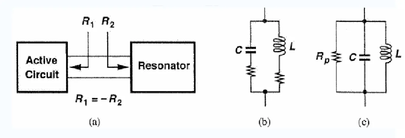
Figure 2.1 (a) Feedback oscillatory system, (b) (a) with frequency selective network
Figure 2.2 (a) One port view of oscillators, (b) LC resonator, (c) equivalent circuit
Figure 2.3 Automatic level control
Figure 2.4 (a) Direct feedback form collector to emitter, (b) insertion of an impedance transformer, (c) use of an explicit transformer
Figure 2.5 (a) Colpitts, (b) Hartley oscillators
Figure 2.6 Clapp oscillator
Figure 2.7 Direct conversion transmitter with offset LO
Figure 2.8 Varactor diodes added to a tank
Figure 2.9 Output spectrum of ideal and actual oscillators
Figure 2.11 (a) Downconversion by an ideal oscillator, (b) reciprocal mixing,(c) Effect of phase noise in transmitters
Figure 2.12 A definition of Q
Figure 2.13 Illustration of frequency tuning characteristics of VCO using a bank of switching capacitors: (a) frequency and (b) VCO gain.
Figure 2.14 Addition of the output voltages of N oscillators
Figure 2.15 Injection pulling of an oscillator as the noise amplitude increases
Figure 2.16 Injection pulling due to large interferer
Figure 2.17 Load pulling due to variation of impedance
Chapter 3 Bipolar and CMOS LC Oscillator
Figure 3.1 (a) Addition of active buffer in feedback loop of a Colpitts oscillator, (b) implementation of buffer with an emitter follower, (c) differential implementation of (b)
Figure 3.2 Circuit to calculate the input impedance of cross-coupled pair
Figure 3.3 Capacitive division in feedback path of an oscillator
Figure 3.4 CMOS oscillators, (a) output referred to VDD, (b) output referred to ground, (c) Differential operation with one inductor
Figure 3.6 Interpolative oscillator using two tanks
Figure 3.7 Open loop gain and phase of an interpolative oscillator
Figure 3.8 21.5/43-GHz Dual Frequency Balanced Colpitts VCO circuit schematic Figure 3.9 Schematic of dual band VCO
Figure 3.10 (a) and (b) Two-use configurations of a switched resonator. (c) An equivalent circuit of a switched resonator in (a). (d) The equivalent circuit when port 2 is ac grounded and the switch is on. (e) The equivalent circuit when the switch is off. Figure 3.11 Two single inductor excitation
Figure 3.12 Differential inductor with center tap excitation Figure 3.13 Inductor equivalent circuit model
Figure 3.14 Spice-like equivalent circuit
Chapter 4 Multi-section Resonator VCO applied for UWB
Figure 4.1Occupied frequency of different protocol
Figure 4.2 Proposal multi-section VCO equivalent circuit Figure 4.3 Simplified LC tank equivalent circuit
Figure 4.4 2.5D EM simulation of Le Figure 4.5 Physical layout of Le
Chapter 5 Summary
Chapter 1
Introduction
1.1 Motivation
Recently, there are many kinds of communication device existing in the world. Such as wireless LAN, cordless and cellular phones, global positioning satellite (GPS) used in car traveling, pagers used in mining, RFID tags used in purchasing and cargo management and so on. Those devices all require low cost, low noise interference and high power efficiency performance to be adaptive.
Communication technique trends to be plural application in this environment. The market of front end system on chip presents a proper growth and its technique has high potentially power consumption consideration, even more on a portable and wireless device. Although high frequency circuit design is always base on GaAs and HBT, utilizes its high fT
and low noise to implement the wireless technique. Base on the cost of manufacture is too high, and the circuit of transceiver’s baseband is made by CMOS fabrication. The above problem causes its complexity of communication system implementation and the area of die is hard to be less. An evolution of CMOS fabrication is scale down in progress, degrades its cost and integrates baseband circuit to be a SOC. This integration radio frequency circuit “RFIC” manufactured by CMOS is to be best solution of wireless communication system. The frequency synthesizer of wireless transceiver provides local oscillation frequency “LO”
to the signal through the path of transmit and receive. The frequency synthesizer generates a periodic and precise clock entering a mixer. Phase noise and tuning range are very important parameter of the quality of communication to VCO and this experiment implements a multi-section resonation tuning range applied in 3.1GHz~10.6GHz [1] [2].
Chapter 2
Oscillators
Beginning with some general issues, consider basic oscillator topologies and phase noise in oscillators. Given the effort expended in avoiding instability in most feedback systems, it would seem trivial to construct oscillators. However, simply generating some periodic output is not sufficient for modern high performance RF receivers and transmitters. Issues of spectral purity and amplitude stability must be addressed.
2.1 General Concepts
Figure 2.1 (a) Feedback oscillatory system, (b) (a) with frequency selective network
Observed an oscillator, it is transparently a periodic generation device. As such, the circuit must entail a self-sustaining mechanism that allows its own noise to grow and eventually become a periodic signal. It can be treated as feedback circuit and consider the simple linear feedback system depicted in Fig 2.1(a), with the overall transfer function, Equation (2.1).
(2.1) XY((ss)) =1−HH(s()s)
A self-sustaining mechanism arises at the frequency
s
0 if , and the oscillatoramplitude remains constant if
s
0 is purely imaginary, i.e., . Thus, for steadyoscillation, two conditions must be simultaneously met at ω0: (1) the loop gain, ,
must be equal to unity, and (2) the total phase shift around the loop, , must be equal to zero (or 180° if the dc feedback is negative). Called Barkhausen’s criteria, the above
conditions imply that any feedback system can oscillate if its loop gain and phase shift are chosen properly. For example, ring oscillators and phase shift oscillators are. In most RF oscillators, however, a frequency selective network called a “resonator”, an LC tank is included in the loop so as to stabilize the frequency in Fig 2.1(b).
1 ) (s0 =+ 0 H ( 0 +
Figure 2.2 (a) One port view of oscillators, (b) LC resonator, (c) equivalent circuit
The nominal frequency of oscillation is usually determined by the properties of the circuit, the resonance frequency of the LC tank in Fig 2.2 (a),(b),(c). But how about the amplitude is? The self-sustaining effect allows the circuit’s noise to grow initially, but another mechanism
) ( jω0 H s0= 1 )= = jω H s H ∠ (jω0)
is necessary to limit the growth at some point. While the amplitude increases, the amplifier saturates, dropping the loop gain to a low value at the peaks of the waveform. From another point of view, to ensure oscillation start-up, the small signal loop gain must be somewhat greater than one, but to achieve a stable amplitude, the average loop gain must return to unity.
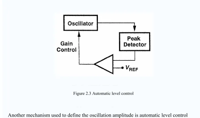
Figure 2.3 Automatic level control
Another mechanism used to define the oscillation amplitude is automatic level control (ALC). Illustrated in Fig 2.3, this technique measures the amplitude by means of a peak detector (or a rectifier), compares the result with a reference, and adjusts the gain of the oscillator with negative feedback. Thus, at the start-up, the amplitude is small and the gain is high, and in the steady state, the amplitude is approximately equal to VREF is chosen properly, providing a sinusoidal output with low distortion. However, the complexity of the circuit and the possibility of additional noise contributed by ALC have prevented wide usage of this technique in RF applications. In physical application, the outputs contain two or more
oscillators is built by differential topologies and this kinds of topologies have a 50% duty circle characteristic.
2.2 Basic LC Oscillator Topologies
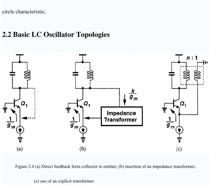
Figure 2.4 (a) Direct feedback form collector to emitter, (b) insertion of an impedance transformer, (c) use of an explicit transformer
This section introduces some basic topologies of oscillators base on “one transistor” and analyzes its structure independently. As shown in Fig 2.4(a), the tank consists of an inductor and a capacitor in parallel. Since at resonance, the impedance of the tank is real, the phase difference between its current and voltage is zero. Thus, to achieve a total phase equal to zero, the feedback signal must return to the emitter of the transistor. This is one kind of basic idea of oscillator topologies. The connection of the LC tank to emitter entails an important issue: the resistive loading seen at the emitter terminal, 1/gm. If the collector voltage is directly
applied to the emitter, this resistance drastically reduces the quality factor “Q” of the tank, dropping the loop gain to below unity and preventing oscillation. Depend on this reason, the emitter impedance must be transformed to higher value before it appears in parallel with the tank, shown as Fig 2.4(b). A simple approach to transforming the emitter impedance is to incorporate a transformer in the tank,Fig 2.4(c). For a lossless step-down transformer with a turn ratio n, the parallel resistance seen by the tank is equal to . Passive impedance transformation can also be accomplished through the use of tanks with capacitive or inductive divider. Illustrated in Fig 2.5(a) and (b), the resulting circuits are called the Colpitts and Hartley oscillators, respectively. The equivalent parallel resistance in the tank is
approximately equal to in Fig 2.5(a) and in Fig 2.5(b),
enhancing the equivalent Q by roughly the same factor.
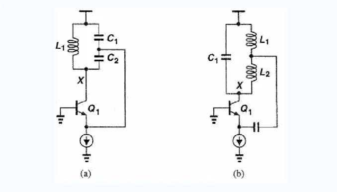
Figure 2.5 (a) Colpitts, (b) Hartley oscillators m g C / / ( ( L /L /g g n / C ) 1 2 2 1 + 1 )2 1 2 + 2 m m
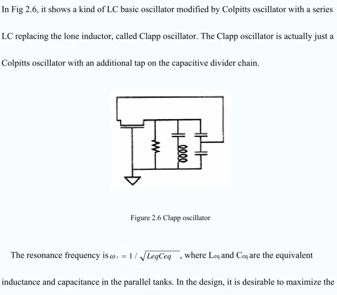
In Fig 2.6, it shows a kind of LC basic oscillator modified by Colpitts oscillator with a series LC replacing the lone inductor, called Clapp oscillator. The Clapp oscillator is actually just a Colpitts oscillator with an additional tap on the capacitive divider chain.
Figure 2.6 Clapp oscillator
The resonance frequency is , where Leq and Ceq are the equivalent
inductance and capacitance in the parallel tanks. In the design, it is desirable to maximize the value of the inductor to achieve large voltage swings. The Q of inductors is typically much lower than that of capacitors, making it possible to write the equivalent parallel resistance of the tank as , where Rs models the loss of the inductor as a series resistance. In typical inductors, Leq and Rs scale proportionally; that is , if Leq increases by a factor m, then so does Rp. Since the impedance of the tank at resonance is equal to Rp, the voltage swing for a given bias current also increases by the same factor. If the inductor is off-chip, increasing its value also minimizes the effect of bond wire inductance, an important issue at frequencies above 1GHz. Transistor Q1 is the primary source of noise in the oscillators of Fig 2.5 and
LeqCeq
r =1/
ω
R Rp/(Leqωr)2/ s
hence plays a important role. The base resistance thermal noise and the collector shot noise can be minimized by increasing the size and decreasing the bias current of the transistor, respectively. However, the first remedy raises the parasitic capacitances, and the second lowers the voltage swing. Thus, a compromise is usually necessary. The bias current is typically chosen to yield maximum swing at node X without saturating Q1 [3] [4].
2.3 Voltage Controlled Oscillators
Figure 2.7 Direct conversion transmitter with offset LO
In a RF system, the frequency must be adjustable depending on well defined steps
frequency of LO to switch in different available channel, shown in Fig 2.7. Output frequency of an oscillator can be varied by a voltage, then this circuit is called a “voltage controlled oscillator”. While current-controlled oscillators are also feasible, they are not widely used in
RF systems because of difficulties in varying the value of high-Q storage elements by means of a current.
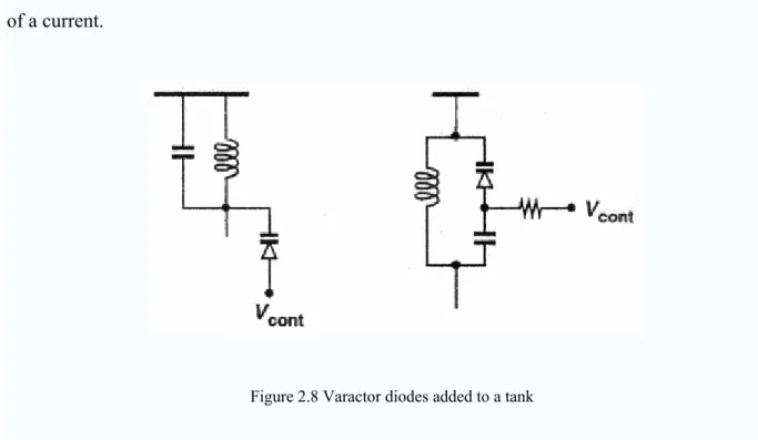
Figure 2.8 Varactor diodes added to a tank
In LC implementations, the tank capacitance can be provided by a reverse-biased diode (varactor) so that the dc voltage across the junction controls the resonance frequency, shown in Fig 2.8. A mathematical model of VCOs, , whereωFR is the
“free running” frequency and Kvco is the “gain” of the VCO. The existence ofωFR in the above
equation simply indicates that, for the practical range of Vcont, ωout may not approach zero. In
other words, Vcont creates a change aroundωFR. Since phase is the integral of frequency with
respect to time, the output of a sinusoidal VCO can be expressed as Equation (2.2).
cont VCO FR out cont K V V :ω =ω +
(
=
cos(
(2.2)+
∫
t)
dt
V
K
A
y
)
ω
FRIn particular, for sinusoidal modulation, , and Equation (2.3).
∞ −
t
t
VCO cont t m m cont V V ( )= cosω t(2.3)
y
(
t
)
A
cos(
FRt
K
V
msin
ω
mt
)
m VCOω
ω
+
=
Indicating that the VCO has tendency to reject high frequency components that appear at its control input. Also, if rad, then the narrowband FM approximation applies, and the output spectrum consists of a main component at and two sidebands at [5] [6]. 1 / << KVCOVm ωm
2.4 Design Considerations
2.4.1 Phase Noise
Figure 2.9 Output spectrum of ideal and actual oscillators
Noise rejection for analog design is always existence problem. If the noise floor raises up, it
influences the modulation signal to be distorted. In most cases, the design only takes care of the random deviation of available frequency and ignores the disturbance in the amplitude. Expressed by a mathematical model, a nominally periodic sinusoidal signal is written as,
FR
whereψn(t) is small random excess phase representing variations in
the period. The functionψn(t) is called “phase noise”. Note that for rad, and
then ; that is, the spectrum ofψn(t) is translated to ±ωc. In RF
applications, phase noise is usually characterized in the frequency domain. In Fig 2.9, an ideal sinusoidal oscillator operating at ωc, the spectrum assumes the shape of an impulse, whereas
for an actual oscillator, the spectrum exhibits “skirts” around the carrier frequency. To quantify phase noise, a unit bandwidth at an offset △ω with respect toωc, calculate the
noise power in this bandwidth and divide the result by the carrier power. The effect of phase noise occupies high proportion of modulation signal in RF communication systems [7].
[
( )]
cos A ) (t t t x = ωc +φn 1 << φ A A x ) (t n t t) cosωc φn(t)sinωct ( = −Figure 2.10 Generic transceiver front end
To understand the importance of phase noise in RF systems, consider a generic transceiver as depicted in Fig 2.10, where a local oscillator provides the carrier signal for both the
transmit and receive paths. If the LO output contains phase noise, both downconverted and upconverted signals are corrupted, shown as Fig 2.11.
Figure 2.11 (a) Downconversion by an ideal oscillator, (b) reciprocal mixing, (c) Effect of phase noise in transmitters
2.4.2 Quality factor of Oscillators
Traditionally, phase noise of LC oscillators usually depends on their Q. Intuitively, higher Q of the LC tank is better, the sharper the resonance and the lower the phase noise skirts. Resonant circuit usually exhibit a bandpass transfer function. The Q can also be defined as the
“sharpness” of the magnitude of the frequency response. In Fig 2.12, Q is defined as the resonance frequency divided by the two side -3 dB bandwidth.
Figure 2.12 A definition of Q
The Si-based radio implementation for a wireless system results in a new environment for the LC tank voltage controlled oscillator, which has been hard to be integrated into a
transceiver because of the poor quality of an on-chip inductor. Great effort has gone into different approaches to overcome this problem. Si-based IC technology has been improved to achieve a high Q inductor. A thick metallization process has been used for the top metal layer to reduce the series resistance of an inductor layer. To minimize the parasitic effects of the substrate, the distance has been increased between the top metal layer and the Si substrate. Recently, special efforts have been focused on growing SiO onto Si substrate. However, all of the above-mentioned approaches to produce a high-Q inductor increase the cost, which is opposite to the reason for which the Si-based solution was proposed in the first place. Si-based micro-electromechanical system (MEMS) technologies have also been used to implement the high-Q inductor. Copper plating provides high conductivity and thick
metallization. Surface micromachining technologies enable the inductor layer to hang over air. The Si substrate effects can be reduced by bulk micromachining technologies. However, even if the MEMS inductor shows a very high-Q characteristic, cost and reliability are obstacles to its commercial adoption [8] [9].
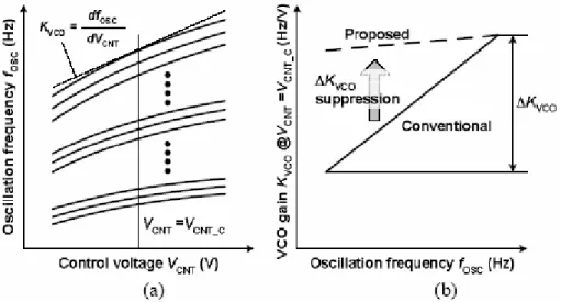
2.4.3 Tuning range and K
VCOof Oscillators
A wide tuning range LC-tuned voltage controlled oscillator featuring small VCO-gain (KVCO) fluctuation was developed. For small KVCO fluctuation, a serial LC-resonator that
consists of an inductor, a fine-tuning varactor, and a capacitor bank was added to a
conventional parallel LC-resonator that uses a capacitor bank scheme. To meet the growing demand for high data-rate communication systems worldwide, cellular phone systems such as W-CDMA must support multi-band or multi-mode operation. For a cost-effective W-CDMA RFIC that supports multi-band UMTS, a single VCO generating LO signals, which has a wide frequency range and attains low phase noise at low power, is a key component. Moreover, to achieve a low phase-noise LO signal when the VCO is included in a phase locked loop (PLL), sensitivity to the noise generated by the PLL’s building blocks must be reduced. VCO gain (KVCO), which is a frequency-conversion gain, must therefore be small.
A general approach to achieving both wide frequency tuning range (∆f) and low KVCO in a
VCO is to use a bank of switching capacitors. However, KVCO fluctuates widely in the
KVCO fluctuation increases with ∆f of the VCO, so it must be suppressed when wide ∆f is
necessary. Suppress KVCO-fluctuation against frequency (∆KVCO) while maintaining ∆f and
without degrading phase noise. Fig 2.13 illustrates oscillation frequency (fOSC) tuning
characteristics of a VCO using a conventional LC-resonator with banks of switching capacitors. Equation (2.4),(2.5) express its fOSC and KVCO of equivalent circuit and L1
represents the inductor of resonator, Cv1 is fine tuning pn-junction varactor, CB11, CB12 and
CB1 are for coarse tuning. fOSC is tuned continuously with CV1 by controlling control voltage
VCNT. The capacitor banks CB11 and CB12 have plural MOS varactors, and the capacitance of
each MOS varactor is changed to be either a maximum or minimum value by controlling voltage Vcoarse. As a result, fOSC is tuned gradually with CB1 by controlling Vcoarse. Therefore,
the VCO exhibits several frequency curves, as illustrated in Fig. 2.12(a) VCO gain (KVCO) is a
frequency conversion gain against VCNT [10] [11].
Figure 2.13 Illustration of frequency tuning characteristics of VCO using a bank of switching capacitors: (a) frequency and (b) VCO gain.
(2.4)
fosc
2
π
L
(
C
)
1
1 1 1C
V+
B=
(2.5) CNT V B V CNT osc VCOdV
L
dV
4
π
(
dC
C
C
df
K
3/2 1 1 1 1.
)
1
.
1
+
=
=
2.4.4 Output Swings of Oscillators
An LC resonator oscillator design applied in RF communication systems. It should be taken into consideration, its output swing matching with mixer to get a high respond gain. A better power transmission point at 0~1 dBm combined with mixer. The experimental result proves output swings restricting within 200 mV in a VCO design. No matter the output swings meet to this condition, it still keeps a stable and constant value. And it always is important for this entire design of oscillators.
2.4.5 Noise Power Trade off
In a physical oscillator design, it is always a trade off between power dissipation and noise. If the output voltages of N identical oscillators are added in phase, shown as Fig 2.14, then the total carrier power is multiplied by N², whereas the noise power increases by N. Thus, the phase noise decreases by a factor N at the cost of proportional increase in power dissipation.
Figure 2.14 Addition of the output voltages of N oscillators
Following parameters must be taken into account, the center frequency
ω
0, the powerdissipation P and the offset frequency △ω. Thus, the phase noise power of different
oscillators must be normalized to (ω0/Δω)2/P for a fair comparison.
2.4.6 Effect of Frequency Division and Multiplication
Since frequency and phase are related by a linear operator, division of frequency by a factor
N is identical to division of phase by the same factor. For a nominally periodic
sinusoid, , where represents the phase noise, a frequency divider simply divides the total phase by N, Equation (2.6).
x /N = Acos ⎡⎢⎣N t + N ⎥⎦⎤ (2.6) t n( ) 1
ω
φ
t) cos[
c n( )]
( A t t x = ω +φ φntwhere the phase noise contributed by divider is neglected. This indicates that magnitude of phase noise at given offset frequency is divided by N, and from narrowband FM
approximation the phase noise power is divided by N². A similar analysis shows that frequency multiplication raises the phase noise magnitude by the same factor.
2.4.7 Pulling and Pushing
Assumed that the magnitude of the noise injected into the signal path is much less than that of the carrier, thereby arriving at a noise shaping function for oscillators. An interesting phenomenon is observed if the injected component is close to the carrier frequency and has a comparable magnitude, shown as Fig 2.15. As the magnitude of the noise increases, the carrier frequency may shift toward the noise frequency ωn and eventually “lock” to that
Figure 2.15 Injection pulling of an oscillator as the noise amplitude increases
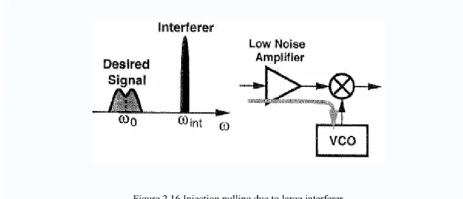
In a transceiver environment, various sources can introduce oscillator pulling. As like a power amplifier output may couple to LO and injection pulling arises in the receive path when the desired signal is accompanied by a large interferer, shown as Fig 2.16. If the interferer frequency is close to the LO frequency, coupling through the mixer may pull ωLO toward
ωint. Thus, the VCO must be followed by a buffer stage with high reverse isolation. However,
the noise of such a stage may increase the noise figure of the mixer.
Figure 2.16 Injection pulling due to large interferer
Fig 2.17 illustrates a GFSK modulator system, a topology used in DECT transmitters. This VCO first placed in a feedback loop so as to stabilize its output frequency. Subsequently, the control voltage of the VCO is switched to the baseband signal, allowing the VCO to function as a frequency modulator. However, the open loop operation makes the VCO frequency quite sensitive to variations in the load impedance “load pulling”. In particular, as the power
amplifier turns on and off periodically to save energy, the VCO center frequency changes considerably, demanding a high isolation stage between the VCO and the PA.
Figure 2.17 Load pulling due to variation of impedance
RF oscillators in general exhibit a poor supply rejection. If the supply voltage varies, so do the reverse to voltage across the varactor and the frequency of oscillation. In RF design, this is called “supply pushing”. An important case of supply pushing occurs in portable transceivers when the power amplifier turns on and off. Owing to the finite output impedance of the battery, the supply voltage may vary by several hundred millivolts.
Chapter 3 Bipolar and CMOS LC Oscillator
This chapter introduces several kinds of LC oscillators fabricated by CMOS and Bipolar. Analyze its topology and equivalent circuit to trace what design issue influences its entire function? Discuss with some novel VCO designs understanding their merit and drawback. Basically, the design considerations of a VCO design always takes care of phase noise, Q and so on. In RF application, it should have a good trade-off between these considerations, as described in chapter 2.
3.1 Negative-G
mOscillators
Figure 3.1 (a) Addition of active buffer in feedback loop of a Colpitts oscillator, (b) implementation of buffer with an emitter follower, (c) differential implementation of (b)
In Fig 3.1, an active buffer B1 is interposed between the collector and the emitter,
presenting a relatively high impedance to the bank. The buffer B1 can be implemented as an
emitter (or source) follower. Note that the base of Q1 is connected to Vcc to have the same dc
voltage as the base of Q2. The circuit can also incorporate two inductors to operate
differentially, shown as Fig 3.1(c). However, if the inductors are off-chip, bond wire parasitics make it difficult to achieve a small phase mismatch between the two tanks.
The feedback oscillator of Fig 3.1(c) can be viewed as a one port implementation as well. Calculating the impedance seen at the collector of Q1 and Q2, shown as Fig 3.2. Note that
positive feedback yield Equation (3.1). Thus, if |Rin| is less than or equal to the equivalent parallel resistance of the tank, the circuit oscillates. This topology is called a “negative-Gm oscillator”.
(3.1) in
g
mR
= /
−
2
In addition to contributing noise, Q1 and Q2 in Fig 3.1(c) saturate heavily if the peak swing
at nodes X and Y exceeds approximately 400 mV. To resolve this issue, a capacitive divider can be inserted in the feedback path, shown as Fig 3.3, allowing greater swings and higher common mode level at nodes X and Y than at the bases of Q1 and Q2.
Figure 3.3 Capacitive division in feedback path of an oscillator
Figure 3.4 CMOS oscillators, (a) output referred to VDD, (b) output referred to ground,
(c) Differential operation with one inductor
3.2 Interpolative Oscillators
The frequency of VCOs can be varied by adjusting the tank capacitance or inductance. An interpolative oscillator provides an alternative tuning mechanism by employing more than one resonator. Fig 3.5 illustrates a feedback oscillatory system incorporating two transfer functions, H1(s) and H2(s), whose outputs are scaled by variable factors α1 andα2,
respectively, and summed. The overall open loop transfer function is therefore equal to H(s)= α1 H1(s)+α2 H2(s), which must equal +1 for the system to oscillate. In the extreme cases
whereα1=0 orα2=0, the oscillation frequency, ωc, is determined by only H1(s) or H2(s), and
for intermediate values ofα1 andα2, ωc can be “interpolated” between its lower and upper
bounds. Of course, this occurs only if the roots of H(s)-1=0 move in a “well-behaved” manner from one extreme to the other.
In Fig 3.6, it shows a conceptual illustration of the oscillator. R1 and R2 denote the
equivalent parallel resistance of each tank. For the system to oscillate, the open loop transfer function must equal unity.
1 + 2 − =0 (3.2) +L R R
R α
α
It assumes Equation (3.2) that has a unique set of conjugate roots on the imaginary axis or in the right half plane, then the circuit oscillates at a single frequency.
Fig 3.7illustrates that the resonance frequencies of the two tanks, ω1 andω2 are far apart.
It plots the open loop gain and phase of such an oscillator, revealing two frequencies at which the total phase is zero and the gain is greater than unity. As a consequence, the circuit may oscillate at more than one frequency. It can be shown that the maximum spacing betweenω1
andω2 that avoids this effect is equal to , where the two tanks are assumed to
have equal Q. Interpolative oscillators exhibit a trade-off between the phase noise and the tuning range. 1 2 2 2 2 2 2 2 2 2 1 1 2 1 1 1 1 1 1 + + + L C s L s R s L R G s s C L s L R Gm m ) 1 /( Q (ω +ω2 2 )
Figure 3.7 Open loop gain and phase of an interpolative oscillator
3.3 Experimental VCO designs
3.3.1 A 21.5/43-GHz Dual Frequency Balanced Colpitts VCO
Figure 3.8 21.5/43-GHz Dual Frequency Balanced Colpitts VCO circuit schematic
The circuit schematic is shown in Fig 3.8. Two single common base Colpitts VCOs are synchronized at the base terminals and through the varactors between the emitter terminals. The resulting balanced VCO operates differentially and virtual ac grounds are formed at the
base terminals and at the node between the varactors. Thus, each half of the balanced VCO circuit behaves like a single Colpitts VCO. The two parts operate in anti-phase at the fundamental frequency, which is collected differentially at the collectors. The second harmonic is probed directly at node, shown in Fig 3.8, where the fundamental frequency components cancel, while the second harmonics add constructively. Four varactors, which are placed between the two emitters, are tuned differentially by Vtune+ and Vtune-, which are
related to the reverse bias across each varactor, Vtune, through, Equation (3.3),
(3.3) e tune tune e tune tune
V
V
V
V
V
V
+
−
=
+
=
− +,where represents the dc voltage at the emitter, which is 0.4 V according to simulation. Common mode noise voltages result in changing capacitance of and in opposite directions, thus leaving the total capacitance of the parallel connection unchanged. This increases the frequency stability, i.e., reduces phase noise when differentially tuned. Simulation shows that the phase noise of a VCO using four varactors is about 3 dB lower than using two varactors. No output buffer is used in this design. The capacitors used for ac coupling to a 50Ohm load resistor are chosen as small as 50 fF to prevent the resonator from being heavily loaded. This is a major reason for the low output power obtained in this design.
In the VCO design, small signal analysis is carried out first. Loop gain and phase shift are estimated with respect to varying inductance, capacitance, transistor size, and bias conditions. The VCO oscillation frequency is then determined by fulfilling the well-known oscillation
conditions, i.e., zero phase shift and larger-than-unity loop gain. Second, harmonic balance analysis is used to calculate the phase noise. The ratio of C1 to C2 is crucial to both phase
noise and loop gain and is chosen carefully by simulations. Relatively large sized transistors are used to reduce the base resistance and minimize 1/f noise. However, a too large transistor size should be avoided, since large parasitic capacitances lower tuning range. Proper bias currents in the VCO are also very important for the phase noise and loop gain. Large currents result in large voltage swings in the resonator, thus reducing phase noise. On the other hand, a transistor operating under large bias currents contribute significant shot noise to the circuit. The voltage swing in the resonator is limited by the breakdown voltage of the transistors. The open-base collector–emitter breakdown voltage, BVCEO, in the technology used here is 2.5 V.
Our VCE simulated has a peak-to-peak value of 3 V. This 20% excess in VCE over the BVCEO
should not raise much reliability concern, since the impedance seen by the base is less than infinity. Finally, optimization is carried out automatically toward low phase noise through fine tuning of the components’ values and bias conditions.
A balanced Colpitts VCO has been presented, which has a 21.5 GHz differential output and a 43 GHz single ended output. Excellent low phase noise characteristics are achieved. This demonstrates the great potential of using the VCO topology presented here for low-cost, low-phase-noise, and high-frequency signal generators, possibly up to 60 GHz [12].
3.3.2 A Switched Resonators Applied in a Dual-Band LC Tuned VCO
A switched resonator concept, which can be used to reduce the size of multiple band RF systems and which allows better tradeoff between phase noise and power consumption, is demonstrated using a dual band voltage controlled oscillator in a 0.18 µm CMOS process. To maximize Q of the switched resonator when the switch is on, the mutual inductance between the inductors should be kept low and the switch transistor size should be optimized. The quality factor of switched resonators is ~30% lower than that of a standalone inductor. This work operates on 0.9 GHz and 1.8 GHz dual band frequency.
Figure 3.9 Schematic of dual band VCO
The proliferation of wireless applications is rapidly increasing the demand for low cost communication terminals, which can support multiple standards and frequency bands. In response to this, multi-band terminals using multiple RF transceivers have been reported. However, increases die area or chip count in a radio, which, in turn, increases cost and
complexity of radios. A way to mitigate this is the use of a tunable/programmable transceiver consisting of a tunable low-noise amplifier, buffers and mixers, and a voltage controlled oscillator with a wide tuning range. To realize the tunable RF blocks, the variable inductor concept has been previously reported and utilized first in a VCO. The VCO partially relies on the changes in series resistance of an inductor to attain continuous variations of effective inductance. This resistance, however, significantly degrades of the resonator and phase noise of the VCO. To reduce the degradation of phase noise, a switched resonator concept, shown as dotted rectangle in Fig 3.9 is proposed and demonstrated in a dual band VCO, and a VCO with a tuning range greater than 50% and excellent phase noise performance. In this work, the measured and simulated characteristics of switched resonators including the quality factor are reported. Analytical expressions, which explain the behaviors of switched resonators, as well as the design considerations and approaches to improve their properties are presented. Lastly, this work suggests that a dual band VCO using switched resonators can have the same phase noise and power consumption while occupying a smaller area than that for two VCOs needed to cover the two bands.
Fig 3.10(a) and (b) shows switched resonators including mutual inductance (M). The inductance seen between ports 1 and 2 are changed by turning the switch transistor Msw on and off. The equivalent circuit of the switched resonator is shown in Fig 3.10 (c). In the case that port 2 is grounded and that L1 and L2 have no mutual effect (M=0), the resonator is
simplified into the circuit in Fig 3.10 (d) when the switch is on, and into the circuit in Fig. 3.10 (e) when off. When the switch is off, the inductance of switched resonator is largely determined by the two inductors while the capacitance is determined by the parasitic
capacitances (CpL1’s and CpL2) of the inductors and the capacitances (Cdb and Cgd) at the drain
of the switch transistor. The extracted inductance using measurements and the simple inductor model is lower due to the effects of Cgd in series with Cgs, and Cdb of the switch transistor
(M4). When the switch is on, the channel resistance is close to zero. The inductance and
capacitance of the switched resonator are switched by shorting out L2, the capacitances
associated with L2, L1, and the switch transistor. The inductance is approximately L1 and the
capacitance is Cp1, thus, leading to simultaneous decreases of inductance and capacitance
Figure 3.10 (a) and (b) Two-use configurations of a switched resonator. (c) An equivalent circuit of a switched resonator in (a). (d) The equivalent circuit when port 2 is ac grounded and the switch is on. (e) The equivalent circuit when the switch is off.
3.3.3 A Low phase noise VCO design with Symmetrical Inductor
When a symmetric inductor is driven differentially, voltages on adjacent conductors are in anti-phase but currents flow in the same direction on each side. This increases the overall magnetic flows as Fig 3.11 and Fig 3.12. The equivalent circuit of inductor is shown in Fig 3.13. In the high frequency operation, the substrate parasitic C and R involved. For the differential excitation, these parasitic effects have higher impedance than in the single-ended
connection. Obviously, this reduces the real part and reactive component of the input
impedance. Therefore, the inductor Q factor is better and yields a wider operating bandwidth. In this work, this argument is well proved by the measurements of single ended and
differential inductors.
Figure 3.11 Two single inductor excitation
Figure 3.13 Inductor equivalent circuit model
The inductor area can be saved as 50% when using differential inductor without sacrificing its performances. The equivalent model as shown in Fig 3.14 can be easily constructed for Spice-like simulator. Something needed to notice here, that the model is three ports. In the differential application, the centre point is a virtual ground as illustrated in port 3. The port 3 can be widely use as the dc supply or ground. Since the advantages of symmetrical
inductors as mentioned before, the symmetrical VCO will be the better choice for a low phase noise design.
Figure 3.14 Spice-like equivalent circuit
The work presented a design methodology of C-band VCO using 0.35 µm CMOS low cost process. The single-ended and symmetrical driven inductors are thoroughly investigated, designed, and measured. A general three port model for a symmetrical driven inductor is well established in this work. These two types’ inductors are applied for the low phase noise VCO design. The symmetrical driven VCO achieves a phase noise of -112dBc/Hz at a frequency offset of 1MHz from the carrier which yields 10 dB improvements in comparison to that of single-ended driven VCO [14].
Chapter 4 Multi-section Resonator VCO applied for UWB
4.1 Introduction of Ultra Wideband
Figure 4.1 Occupied frequency of different protocol
The release of the first worldwide official ultra-wideband (UWB) emission masks by the U.S. Federal Communication Commission (FCC) in February 2002 opened the way, at least in the U.S., to the development of commercial UWB products. The strong power limitations set by the FCC determined as a natural consequence the application scenarios suitable for UWB communications, that is, either high data rates (HDRs) over short ranges, dealt with by the IEEE 802.15.3a Task Group, or low data rates (LDRs) over medium-to-long ranges, within the IEEE 802.15.4a Task Group.
Different UWB high data rate physical layer (HDR-PHY) submissions to the 802.15.3a Task Group converged into two main proposals: the multi-band orthogonal frequency division multiplexing (MB-OFDM) solution, based on the transmission of continuous OFDM signals combined with frequency hopping (FH) over instantaneous frequency bandwidths of 528 MHz, and the direct-sequence (DS) UWB proposal, based on impulse radio transmission of UWB DS-coded pulses. As the main focus targeted HDR, final standard specifications
lacked requirements on ranging, while a well-known feature of UWB is to allow accurate distance estimation and potentially enable joint communications and ranging. In any case, both MB-OFDM and DS-UWB adopt bandwidths exceeding 500 MHz for UWB emissions in compliance with the UWB definition given by the FCC and can thus provide, when specified, high ranging accuracy.
The UWB good ranging potential was particularly emphasized for location-aware
applications in ad-hoc and sensor networks; the introduction of positioning in LDR networks forms the main concern of the recent IEEE 802.15.4a Task Group, and impulse radio UWB (IR-UWB) radio was proposed as a possible radio transmission technique [15].
4.2 Proposal VCO design
Figure 4.2 Proposal multi-section VCO equivalent circuit
Base on considering the coverage range of Ultra Wideband and saving the area of physical layout, refer to section 3.3.2 and 3.3.3. If this work uses different single inductance to fulfill this bandwidth 3.1 GHz~10.6 GHz, its die will enlarge very much and mutual inductance will be unpredictably causing electrical characteristic dropping. The proposal circuit schematic is shown as Fig 4.2. It generates four different sections of resonating frequencies, because of tuning range limitation, to assemble the entire frequency bandwidth. Le1 andLe2 are
inductance adjustable to this proposal LC tank. Note that deciding an inductor to afford the bandwidth 3.0 GHz~4.0 GHz, and this inductor should have high Q factor to be a high equivalent resistance of this LC tank, shown in Fig 4.3.
Figure 4.3 Simplified LC tank equivalent circuit
(4.1) Req= (1+Q2)×R
The three sections built on the same model of L, Req, Equation (4.1), to each section
inductance still keeps enough to feed start-up oscillation condition, . Q factor, line width, inductance and mutual inductance must be taken into consideration in this
proposal design. Utilize Ansoft designer V2 to analyze the EM effect of Le1 andLe2 modified
by inductor model type “standard“ of TSMC 0.18μm, shown in Fig 4.4.
q
g R
2 ≥ − / m e
Figure 4.4 2.5D EM simulation of Le
This Le model owns 5 port with mutual inductance effect and parasitic effect between port and port. Finally, an equivalent 5 ports’ inductor built on the same area. It really saves the finite space of physical layout and efficiently solves inadequate tuning range to afford bandwidth 3.1 GHz~10.6 GHz, physical layout Le shown as Fig 4.5. An LC tank includes inductors and capacitors to resonate wanted resonating frequency.
The variation resonating frequency of VCO always varies the capacitance of LC tank. It has two kinds of method, one is per providing different operating voltage of transistors to
generating different kind of parasitic capacitance, the other is directly varying the capacitance of LC tank. For this design, method two is chosen and it can keep the output swing and power in constant. Capacitors VC1 and VC2 adopt varactor, g=3 and b=14, can afford all different
section of LC tank to resonate. The above discusses all of LC tank resonator. Another key issue that causes resonating is active component, in Fig 4.2 M1 and M2, cross coupled pair
provides a negative resistance Rin, shown in Equation (3.1). This current steer of LC tank always keeps transistors in saturation region. Under the condition of starting oscillating, the LC tank’s equivalent resistance, Equation (4.1), must be larger than absolute value of Rin. The output buffer adopts a constant current source, avoiding the variation of voltage to reflect on current and this output buffer should take into account degrading the parasitic capacitance as could as possible. To satisfy all of above consideration of a VCO design, the Multi-section inductor CMOS LC-tuned VCO applied for UWB is presented [16] [17] [18] [19].
4.3 The Simulation and Experimental result
Simulation result of each section inductors, as shown in Fig 4.7, 4.8, 4.9, 4.10.
Figure 4.7 Nr=4.25 turns phase noise and tuning range
Freq. tuning range 3.2GHz~4.5GHz Output buffer swing=0.35 V
Figure 4.8 Nr=3 turns phase noise and tuning range
Freq. tuning range 4.65GHz~6.8GHz Output buffer swing=0.35 V
Figure 4.9 Nr=2.25 turns phase noise and tuning range
Freq. tuning range 6.4GHz~9.6GHz Output buffer swing=0.5 V
Figure 4.10 Nr=2 turns phase noise and tuning range
Freq. tuning range 7GHz~10.6GHz Output buffer swing=0.55 V
Expertimental result of each section inductors, as shown in Fig 4.11, 4.12, 4.13, 4.14. 0 . 5 1 . 0 1 .5 2 . 0 2 . 5 3 .0 3 .5 2 .2 2 .3 2 .4 2 .5 2 .6 2 .7 Fr eq (GHz) V c tr l( V ) N r = 4 .2 5
Figure 4.11 Nr=4.25 turns (a) phase noise and, (b) tuning range.
Freq. tuning range 2.2 GHz~2.7GHz Output buffer swing=0.63 V
0 . 5 1 . 0 1 . 5 2 . 0 2 . 5 3 . 0 3 . 5 3 . 2 3 . 4 3 . 6 3 . 8 4 . 0 4 . 2 Fr e q (G H z ) V c t r l( V ) N r = 3
Figure 4.12 Nr=3 turns (a) phase noise and, (b) tuning range.
Freq. tuning range 3.3 GHz~4.1GHz Output buffer swing=0.66 V
0 .5 1 .0 1 .5 2 .0 2 .5 3 .0 3 .5 3 .0 3 .1 3 .2 3 .3 3 .4 3 .5 3 .6 3 .7 3 .8 Fr e q (G H z ) V c tr l( V ) N r = 2 .2 5
Figure 4.13 Nr=2.25 turns (a) phase noise and, (b) tuning range.
Freq. tuning range 3.0 GHz~3.75GHz Output buffer swing=0.63 V
0 . 4 0 . 6 0 . 8 1 . 0 1 . 2 1 . 4 1 . 6 1 . 8 2 . 0 2 . 2 2 . 4 3 . 0 3 . 1 3 . 2 3 . 3 3 . 4 3 . 5 Freq(G H z) V c t r l( V ) N r = 2
Figure 4.14 Nr=2 turns (a) phase noise and, (b) tuning range.
Freq. tuning range 3.0 GHz~3.45GHz Output buffer swing=0.63 V
Chapter 5
Summary
The results have much difference between simulation and experiment. That is because the wafer needs bond-wire to a test board, shown in Fig 5.1, for measuring variation of VDD,
VG, and VCTRL. Bond-wire per each pad has a little parasitic inductance, and it combines with
original existence inductance to be a bigger load. An equivalent Le inductor has a crack that the four ports should not be overlapping in layout, Nr=2 to Nr=3 and Nr=2.25 to Nr=4.25. To analyze the experiment results, it shows that resonated tuning range transparently shifts to low frequency tuning range. In ADS simulation, frequency tuning range Nr=2 is higher than Nr=3, but experimental result is opposite. The overlap ports utilize different metal to connect with varactors in layout. The space between metal 4 and metal 6 causes a capacitance effect. It also enlarges the capacitance load of LC tank. And the inductor model is not ideal as like
simulation.
Parameter This work VCO(Nr=4.25) This work VCO(Nr=3) This work VCO(Nr=2.25) This work VCO(Nr=2) Current 6mA(all circuit) 9mA(all circuit) 6mA(all circuit) 9mA(all circuit)
Tuning Range 2.2GHz~2.7GHz (500MHz) 3.3GHz~4.1GHz (800MHz) 3GHz~3.75GHz (750MHz) 3GHz~3.45GHz (450MHz) Phase noise(1MHz) -112 dBc/MHz -108 dBc/MHz -107 dBc/MHz -108 dBc/MHz Die Size(mm^2) 1.237x0.693 1.237x0.693 1.237x0.693 1.237x0.693
Reference
[1] P.Milozzi, K. Kundert, K. Lampaert, P. Good, and M. chian, ”A design system for RFIC: Challenges and solutions.” Proceedings of the IEEE, Oct.2000.
[2] Philip A. Dafesh, Paul Hanson and Robert Yowell, The Aerospace Corporation ; Tom Stansell, Consultant to The Aerospace Corporation, “A Portable UWB to GPS Emission Simulator.” IEEE 2004.
[3] Shao-Hua Lee, Yun-Hsueh Chuang, Sheng-Lyang Jang, Senior Member, IEEE, and Chien-Cheng Chen “Low-Phase Noise Hartley Differential CMOS Voltage Controlled Oscillator”, IEEE MICROWAVE AND WIRELESS COMPONENTS LETTERS, VOL. 17, NO. 2, FEBRUARY 2007.
[4] Akira Shibutani, Takahiko Saba, Member, IEEE, Seiichiro Moro, Student Member, IEEE, and Shinsaku Mori, Member, IEEE “Transient Response of Colpitts-VCO and
Its Effect on Performance of PLL System”, IEEE TRANSACTIONS ON CIRCUITS AND SYSTEMS—I: FUNDAMENTAL THEORY AND APPLICATIONS, VOL. 45, NO. 7, JULY 1998.
[5] “RF MICROELECTRONICS”, Behzad Razavi. University of California, Los Angeles.
[6] “The Design of CMOS Radio-Frequency Integrated Circuit 2nd edition”, Thomas H. Lee. [7] Sangsoo Ko, Student Member, IEEE, and Songcheol Hong, Member, IEEE “Noise Property of a Quadrature Balanced VCO”, IEEE MICROWAVE AND WIRELESS
COMPONENTS LETTERS, VOL. 15, NO. 10, OCTOBER 2005.
[8] Sang-Woong Yoon, Member, IEEE, Stéphan Pinel, Member, IEEE, and Joy Laskar,
Fellow, IEEE, “High-Performance 2-GHz CMOS LC VCO With High-Q Embedded
Inductors Using Wiring Metal Layer in a Package.” IEEE TRANSACTIONS ON ADVANCED PACKAGING, VOL. 29, NO. 3, AUGUST 2006.
[9] Satoshi Hamano, Kenji Kawakami, and Tadashi Takagi Mitsubishi Electric Corporation, 5-1-1 Ofuna, Kamakura, Kanagawa, 247-8501, JAPAN “A Low Phase Noise 19 GHz-band VCO using Two Different Frequency Resonators”, IEEE 2003.
[10] Takahiro Nakamura, Toru Masuda, Nobuhiro Shiramizu, and Katsuyoshi Washio Central Research Laboratory, Hitachi, Ltd. Kokubunji, Japan; Tomomitsu Kitamura, and Norio Hayashi Renesas Technology, Corp. Gunma, Japan “A Wide-tuning-range VCO with Small VCO-gain Fluctuation for Multi-band W-CDMA RFIC”, IEEE 2006.
[11] Paavo Väänänen, Niko Mikkola, and Petri Heliö “VCO Design With On-Chip Calibration System”, IEEE TRANSACTIONS ON CIRCUITS AND SYSTEMS—I: REGULAR PAPERS, VOL. 53, NO. 10, OCTOBER 2006.
[12] Mingquan Bao, Yinggang Li, Member, IEEE, and Harald Jacobsson, Member, IEEE “A 21.5/43-GHz Dual-Frequency Balanced Colpitts VCO in SiGe Technology”, IEEE
JOURNAL OF SOLID-STATE CIRCUITS, VOL. 39, NO. 8, AUGUST 2004.
Dual-Band Monolithic CMOS LC-Tuned VCO”, IEEE TRANSACTIONS ON MICROWAVE THEORY AND TECHNIQUES, VOL. 54, NO. 1, JANUARY 2006. [14] Hsin-lung Tu, Tsung-Yu Yang and Hwann-Kaeo Chiou Dept. of Electrical Engineering National Central University, Jhongli, Taiwan, ROC “Low phase noise VCO design with Symmetrical Inductor in CMOS 0.35-µm Technology”, IEEE 2005.
[15] UWB Ranging Accuracy in High- and Low-Data-Rate Applications; Roberta Cardinali, Luca De Nardis, Member, IEEE, Maria-Gabriella Di Benedetto, Senior Member, IEEE, and Pierfrancesco Lombardo.
[16] Seong-Mo Yim and Kenneth K. 0 “Demonstration of a Switched Resonator Concept in a Dual-Band Monolithic CMOS LC-nned VCO”, IEEE 2001 CUSTOM INTEGRATED CIRCUITS CONFERENCE.
[17] Frank Herzel, Heide Erzgraber and Nikolay Ilkov Institute for Semiconductor Physics (IHP), Walter-Korsing-Str. 2 15230 Frankfurt (Oder), Germany “A New Approach to Fully Integrated CMOS LC-Oscillators with a Very Large Tuning Range”, IEEE 2000 CUSTOM INTEGRATED CIRCUITS CONFERENCE.
[18] Piljae Park, Cheon Soo Kim, Member, IEEE, Mun Yang Park, Sung Do Kim, and Hyun Kyu Yu, Senior Member, IEEE “Variable Inductance Multilayer Inductor With MOSFET Switch Control”, IEEE ELECTRON DEVICE LETTERS, VOL. 25, NO. 3, MARCH 2004. [19] Jussi Ryynänen, Student Member, IEEE, Kalle Kivekäs, Student Member, IEEE, Jarkko
Jussila, Student Member, IEEE, Aarno Pärssinen, Member, IEEE, and Kari A. I. Halonen “A Dual-Band RF Front-End for WCDMA and GSM Applications”, IEEE JOURNAL OF SOLID-STATE CIRCUITS, VOL. 36, NO. 8, AUGUST 2001.