oxide stack as the gate dielectric, the NW devices could also serve as nonvolatile Si–oxide–nitride–oxide–Si (SONOS) memory de-vices. Our results indicate that the combination of trigate and NW channels help to improve the device performance in terms of step-pers subthreshold swing and reduced threshold voltage. Improve-ment in programming and erasing efficiency of the nonvolatile SONOS memory devices is also demonstrated with the trigated NW structure.
Index Terms—Field-effect transistor, multiple gate, nanowire (NW), poly-Si, Si–oxide–nitride–oxide–Si (SONOS).
I. INTRODUCTION
A
FTER decades of research and development efforts, thin-film transistors (TFTs) fabricated on insulating substrates have become fundamental building blocks for large-area elec-tronics such as flat-panel display. Among several TFT tech-nologies, poly-Si one is especially attractive. Due to the great improvement in film crystallinity over the amorphous counter-parts, poly-Si TFTs exhibit high carrier mobility and make pos-sible the integration of other circuit components like the driver, digital-to-analog (D–A) converters, controllers, processors, and even memories on the same panel [1]. The so-called system-on-panel (SOP) approach not only improves the performance and reliability, but also reduces the manufacturing cost.Certainly poly-Si TFTs face several challenges that need to be carefully addressed. One of them is related to the granular structure of the poly-Si films. The presence of grain bound-aries in the film may impede the carrier transport. Moreover, defects presenting in the grain boundaries act as charge trap-ping centers. For conventional TFT structures having a planar thin film as the channel, the abundant defects contained in the channel tend to retard the gate modulation of the channel sur-Manuscript received February 11, 2009. Date of publication August 25, 2009; date of current version May 14, 2010. The review of this paper was arranged by Associate Editor Lars-Erik Wernersson. This work was supported in part by the National Science Council of the Republic of China (ROC) under Contract NSC 96-2221-E-009-212-MY3.
H.-C. Lin is with the Department of Electronics Engineering and Institute of Electronics, National Chiao Tung University, Hsinchu 300, Taiwan. He is also with the National Nano Device Laboratories, Hsinchu 300, Taiwan (e-mail: [email protected]).
T.-W. Liu, H.-H. Hsu, and T.-Y. Huang are with the Department of Electron-ics Engineering and Institute of ElectronElectron-ics, National Chiao Tung University, Hsinchu 300, Taiwan.
C.-D. Lin is with the National Nano Device Laboratories, Hsinchu 300, Taiwan.
Color versions of one or more of the figures in this paper are available online at http://ieeexplore.ieee.org.
Digital Object Identifier 10.1109/TNANO.2009.2029573
increase the operation voltage needed to achieve the required drive performance, accompanied by the penalty of larger power consumption. Such concern also stands for thin-film memory devices that usually require high voltages for programming and erasing (P/E) operations.
A useful approach to overcome the negative impacts of the granular structure of the poly-Si film is to reduce the total amount of defects by thinning down the channel body. In line with this, poly-Si nanowire (NW) transistors were recently pro-posed and demonstrated to exhibit steep subthreshold swing (∼100 mV/dec or smaller), small threshold voltage, and high ON/OFF current ratio (>107) [2]–[7]. Concurrently, NW Si– oxide–nitride–oxide–Si (SONOS) devices have recently been demonstrated as a good candidate for high-density nonvolatile memory applications [8], [9]. Due to the high surface-to-volume ratio of the NW channel, the P/E operation could be performed at a lower voltage and much faster speed over the planar counter-part [8]. However, the fabrication of the NW devices typically requires advanced lithographic tools and/or complicated pro-cess flow. These are not compatible with the manufacturing of flat-panel products where the device feature size is generally several micrometers or larger. In this paper, we propose a sim-ple and cost-effective approach to fabricate planar poly-Si TFTs and trigated poly-Si NW SONOS devices simultaneously with-out resorting to advanced lithographic tools. Greatly enhanced P/E speed with the proposed trigated NW structure is clearly demonstrated.
II. DEVICEFABRICATION
Fig. 1 shows the process sequence to fabricate simultaneously planar poly-Si TFTs together with the trigated NW SONOS de-vices. In addition to the cross-sectional view of the completed device structure at each step, the top views of device layout at some key steps are also shown to help elucidate the pro-cess features. The fabrication began on Si wafers capped with thermal oxide to simulate the glass substrate. First, a 50-nm-thick tetraethoxysilane (TEOS) oxide and a 50-nm-50-nm-thick silicon nitride were deposited on the wafer surface sequentially by low-temperature chemical vapor deposition [LPCVD, as shown in Fig. 1(a)]. Next, an anisotropic etching step was performed to etch the nitride and TEOS oxide, and form a dummy struc-ture, as shown in Fig. 1(b). Then, an HF-based wet etching step was performed to selectively remove the TEOS layer and form cavities underneath the nitride at the sidewalls of the dummy structure [see Fig. 1(c)], followed by the deposition of an 1536-125X/$26.00 © 2009 IEEE
Fig. 1. Process flow for the simultaneous fabrication of the planar and NW SONOS devices. Top views at some key steps are shown in the right side. The straight lines denote the direction corresponding to the cross-sectional views shown in the left.
amorphous silicon (a-Si) layer by LPCVD [see Fig. 1(d)]. In this step, the cavities were fully refilled with the a-Si layer that was subsequently transformed into polycrystalline phase by solid-phase crystallization (SPC) treatment (at 600◦C in N2ambient for 12 h). Then, a lithographic step was used to define the active regions including the source/drain (S/D) and channel for both planar and NW devices, followed by an anisotropic etching step to define the active region [see Fig. 1(e)]. Afterwards, the Si lay-ers remaining in the cavities snugly formed the NW channels once the top hard mask and side TEOS oxide were selectively removed [see Fig. 1(f)]. Then, an oxide–nitride–oxide (ONO) (4 nm/7 nm/13 nm) stack and an n+ poly-Si layer were sequen-tially deposited. Gate formation was subsequently performed. Self-aligned phosphorous ion implant (30 keV, 1015cm−2) was executed to dope the S/D region [see Fig. 1(g)]. After the S/D activation step, a passivation oxide layer was deposited to cover the fabricated devices, followed by normal metallization proce-dure to form the test pads.
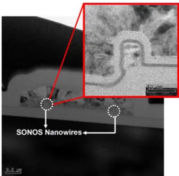
A transmission electron microscopic (TEM) picture of a NW SONOS device is shown in Fig. 2. The height and width of the NW are around 50 and 25 nm, respectively. From the enlarged view of the structure, we can see that the NW is trigated by the conformal ONO and the n+ poly-Si layers. It should be noted that at one side of the NW, the underlying oxide layer is recessed as a result of the etching step stated in Fig. 1(f) during fabrication.
Fig. 2. Cross-sectional TEM image of a NW SONOS device.
III. ELECTRICALCHARACTERISTICS
With the proposed scheme, both planar and NW TFTs can be fabricated simultaneously and integrated easily on the same panel. Typical subthreshold and output characteristics of pla-nar and NW devices are shown in Figs. 3 and 4, respectively. The use of ONO as the gate dielectric for the planar TFTs has been described previously [10]. Well-behaved device character-istics are indeed demonstrated in this paper. More importantly, the NW device shows steeper subthreshold swing and better ON/OFFcurrent ratio than the planar one. This is attributed to the trigated configuration, which provides better gate controllabil-ity over the channel potential [11], and the use of NW channels with significantly reduced defects [12]. In addition, much bet-ter control over the device fluctuation is demonstrated with the NW structure, as shown in Fig. 5. As has been pointed out in one of our previous studies [13], such improvement is again attributed to the shrinkage of channel volume with the NW structure.
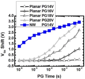
For P/E operations, a high voltage is applied to the gate, while the source and drain are both grounded. Fig. 6 shows the VT H shift versus programming time of NW SONOS devices with gate bias ranging from 11 to 14 V. In this study, VT H is simply defined as the gate voltage at a drain current of 10−9 A. For a fixed period, the VT H shift increases with increasing gate bias. It can be seen that a memory window of 3 V can be achieved within 1 ms with an applied voltage of 14 V, as shown in Fig. 7. We apply this operation condition to program fresh devices to study the erasing characteristics. Fig. 8 shows the results of
VT H shift as a function of erasing time with gate bias of−9,
−10, and −11 V, respectively. The VT H shift increases with increasing magnitude (i.e., absolute value) of the gate voltage and/or operation time. It can be seen that the rate of VT H shift slows down when erasing time is longer than 100 ms with gate
Fig. 3. (a) Subthreshold and (b) output characteristics of a planar device.
Fig. 4. (a) Subthreshold and (b) output characteristics of a NW SONOS device.
Fig. 5. Pelgrom plot indicating that the NW SONOS devices exhibit improved
VT Hfluctuation control.
Fig. 6. VT Hshift as a function of programming (PG) time for NW SONOS
devices stressed under different voltage. (L = 0.7 µm).
Fig. 7. Fresh and programmed subthreshold characteristics of NW SONOS devices. (L = 0.7 µm).
bias of−11 V. This is probably due to the injection of electrons from the gate, and can be alleviated with the adoption of gate electrode with a high work function [14].
Fig. 9 compares the programming characteristics of planar and NW SONOS devices. To compare the programming capa-bility, we apply the same gate bias of 14 V to both planar and NW devices. For the NW one, VT H shift is over 1 V when the
Fig. 8. VT Hshift as a function of erasing (ER) time for NW SONOS devices
stressed under different voltage.
Fig. 9. VT Hshift as a function of programming time for NW (L = 0.7 µm)
and planar (L/W = 0.7/5 µm) SONOS devices stressed under different voltage.
Fig. 10. VT H shift as a function of erasing time for NW (L = 0.7 µm) and
planar SONOS (L/W = 0.7/5 µm) devices stressed under different voltage.
programming time is merely 1 µs. On the contrary, VT Hshift of the planar device is less than 0.1 V even when the programming time increases to 10 ms. In order to obtain the same VT H shift as the NW device at 10 ms, a gate bias of 20 V is needed for the planar device. Similar trends also occur in the erasing character-istics, as shown in Fig. 10. If we apply gate voltage of−11 V to
Fig. 11. Retention characteristics of NW SONOS devices characterized at different temperature. L = 0.7 µm.
Fig. 12. Endurance characteristics of NW SONOS devices under two P/E conditions. L = 0.7 µm.
the planar device for 1 s, the programmed device exhibits only negligible shift. To attain comparable erasing speed to that of the NW device biased with gate voltage of−11 V, the gate bias of the planar device must be raised to−20 V. The aforementioned findings and comparisons on P/E characteristics between planar and NW devices are basically consistent with those previously reported for devices with monocrystalline Si NW channels. Im-proved P/E efficiency with the use of NW channels is attributed to the enhanced carrier injection through the channel due to the enhanced field strength at the channel surface [9].
Data retention characteristics of fresh devices measured at 25◦C and 85◦C, respectively, are shown in Fig. 11. If we pro-gram the devices with gate bias of 13 V for 1 ms, and−11 V with 50 ms for erasing, the memory window can be around 0.8 V after ten years at room temperature. Moreover, the temperature dependence of memory window at ten years is weak. The weak temperature dependence tends to imply that the data lost paths of the fabricated NW SONOS devices are through Frenkel–Poole emission and tunneling effect.
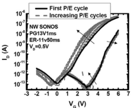
The endurance characteristics are shown in Fig. 12. It is seen that the P/E cycles can be more than 104with acceptable memory window. Nevertheless, window opening is observed in our NW SONOS devices. The memory windows in the beginning are about 1.39 and 2.29 V for the two P/E conditions specified in
Fig. 13. Evolution of subthreshold characteristics of NW SONOS devices with increasing P/E cycles. The arrows indicate the evolution direction. (L = 0.7 µm).
Fig. 14. Retention characteristics of NW SONOS devices after 104P/E cycles. Results for fresh device are also included for comparison. (L = 0.7 µm).
the figure. As stressing cycles increase, the windows extend from 1.39 and 2.29 V to 1.98 and 2.96 V, respectively. Note that the window opening is due to an increase in VT Hof the programmed state and a decrease in VT Hof the erased state. To gain insights into the origins, we also measured and inspected the evolution of subthreshold characteristics during the P/E operations. Fig. 13 shows the ID–VG characteristics of the device corresponding
to the measured points shown in Fig. 12. The arrows contained in the figure indicate the evolution of the I–V curves. In the figure, we conclude that the increase in subthreshold swing due to the generation of interface states is responsible for the increase in VT H of the programmed state. In Fig. 13, we also observe a negative shift in VT H of the erased state, implying the occurrence of hole trapping in the gate dielectric. To make it clear, we also characterized the retention characteristics of the device after 104 P/E cycles. The results are shown in Fig. 14, together with the retention characteristics of a fresh device as a reference. It can be seen that, for the stressed device in the erased state, most of the negative VT H shift recovers within the first 1000 s. This indicates that most of the trapped holes are located close to the oxide/channel interface.
in the future.
REFERENCES
[1] S. Uchikoga, “Low-temperature polycrystalline silicon thin-film transistor technologies for system-on-glass displays,” MRS Bull., vol. 27, pp. 881– 886, Nov. 2002.
[2] M. Im, J.-W. Han, H. Lee, L.-E. Yu, S. Kim, S. C. Jeon, K. H. Kim, G. S. Lee, J. S. Oh, Y. C. Park, H. M. Lee, and Y.-K. Choi, “Multiple-gate CMOS thin-film transistor with polysilicon nanowire,” IEEE Electron
Device Lett, vol. 29, no. 1, pp. 102–104, Jan. 2008.
[3] Y. Shan and S. J. Fonash, “Self-assembling silicon nanowires for device applications using the nanochannel-guided “Grow-in-Place” approach,”
ACS Nano, vol. 2, no. 3, pp. 429–434, 2008.
[4] N. Singh, A. Agarwal, L. K. Bera, T. Y. Liow, R. Yang, S. C. Rustagi, C. H. Tung, R. Kumar, G. Q. Lo, N. Balasubramanian, and D. L. Kwong, “High-performance fully depleted silicon nanowire (diameter≤ 5 nm) gate-all-around CMOS devices,” IEEE Electron Device Lett, vol. 27, no. 5, pp. 383–386, May 2006.
[5] K. H. Cho, S. D. Suk, Y. Y. Yeoh, M. Li, K. H. Yeo, D. W. Kim, D. Park, W. S. Lee, Y. C. Jung, B. H. Hong, and S. W. Hwang, “Temperature-dependent characteristics of cylindrical gate-all-around twin silicon nanowire MOSFETs (TSNWFETs),” IEEE Electron Device
Lett, vol. 28, no. 12, pp. 1129–1131, Dec. 2007.
[6] H. C. Lin, M. H. Lee, C. J. Su, T. Y. Huang, C. C. Lee, and Y. S. Yang, “A simple and low-cost method to fabrication TFTs with poly-Si nanowire channel,” IEEE Electron Device Lett., vol. 26, no. 9, pp. 643–645, Sep. 2005.
[7] H. C. Lin, H. H. Hsu, C. J. Su, and T. Y. Huang, “A novel multiple-gate polycrystalline silicon nanowire transistor featuring an inverse-T gate,” IEEE Electron Device Lett., vol. 29, no. 7, pp. 718–720, Jul. 2008.
[8] S. D. Suk, K. H. Yeo, K. H. Cho, M. Li, Y. Yeoh, K.-H. Hong, S. H. Kim, Y. H. Koh, S. Jung, W. J. Jang, D. W. Kim, D. Park, and B.-I. Ryu, “Gate-all-around twin silicon nanowire SONOS memory,” in Proc. Symp. VLSI
Technol., 2007, pp. 142–143.
[9] J. Fu, N. Singh, K. D. Buddharaju, S. H. G. Teo, C. Shen, Y. Jiang, C. Zhu, M. B. Yu, G. Q. Lo, N. Balasubramanian, D. L. Kwong, E. Gnani, and G. Baccarani, “Si-nanowire based gate-all-around nonvolatile SONOS memory cell,” IEEE Electron Device Lett., vol. 29, no. 5, pp. 518–521, May 2008.
[10] S.-I. Hsieh, H.-T. Chen, Y.-C. Chen, C.-L. Chen, J.-X. Lin, and Y.-C. King, “Reliability and memory characteristics of sequential laterally solidified low temperature polycrystalline silicon thin film transistors with an oxide-nitride-oxide stack gate dielectric,” Jpn. J. Appl. Phys., vol. 45, pp. 3154– 3158, 2006.
[11] H. H. Hsu, H. C. Lin, K. H. Lee, J. F. Huang, and T. Y. Huang, “Character-istics of poly-Si nanowire transistors with multiple-gate configurations,” in Proc. Tech. Dig. VLSI Technol. Syst., Appl., 2008, pp. 101–102. [12] H. C. Lin, K. L. Yeh, M. H. Lee, W. Lee, W. J. Lin, and T. Y. Huang,
“Am-bipolar Schottky barrier poly-Si thin-film transistors with narrow channel width for improved performance,” in Tech. Dig. 2003 Int. Workshop on
Active-matrix Liquid Crystal Displays (AMLCD), Jul., p. 247.
[13] H. H. Hsu, H. C. Lin, L. Chan, and T. Y. Huang, “Threshold voltage fluctuation of double-gated poly-Si nanowire field-effect transistor,” IEEE
Electron Device Lett., vol. 30, no. 3, pp. 243–245, Mar. 2009.
[14] C. H. Lee, K. I. Choi, M. K. Cho, Y. H. Song, K. C. Park, and K. Kim, “A novel SONOS structure with TaN metal gate for multi-giga bit flash memories,” in Proc. IEDM Tech. Dig., 2003, pp. 613–616.
Horng-Chih Lin (S’90–M’95–SM’01) was born in
I-Lan, Taiwan, on August 1, 1967. He received the B.S. degree from the Department of Physics, National Central University, Chung-Li, Taiwan, in 1989, and the Ph.D. degree from the Institute of Electronics, National Chiao Tung University (NCTU), Hsinchu, Taiwan, in 1994.
From 1994 to 2004, he was with the National Nano Device Laboratories, where he was engaged in the research projects of nanoscale device technology development. He joined the faculty of NCTU in 2004, where he is currently a Professor in the Department of Electronics Engineering and the Institute of Electronics. His current research interests include thin-film transistor fabrication and characterization, reliability of CMOS devices, and nanowire device technology. He has authored or coauthored more than 100 technical papers in international journals and conferences.
Dr. Lin was a member of the Program Committee of the International Reliabil-ity Physics Symposium during 2001 and 2002, and the International Conference on Solid State Devices and Materials from 2005 to 2008.
Ta-Wei Liu was born in Changhua, Taiwan. He
received the B.S. degree in materials science and engineering and the M.S. degree from the Insti-tute of Electronics Engineering, National Chiao-Tung University, Hsinchu, Taiwan, in 2006 and 2008, respectively.
He is currently with the Institute of Electronics, National Chiao Tung University. His current research interests include nanowire thin-film transistors fabri-cation and characteristic fluctuation.
Hsing-Hui Hsu was born in Taipei, Taiwan, in 1982.
He received the B.S. degree in electrical engineering in 2004 from National Taiwan University, Taipei, and the M.S. degree in 2008 from the Institute of Elec-tronics, National Chiao-Tung University (NCTU), Hsinchu, Taiwan, where he is currently working to-ward the Ph.D. degree at the Institute of Electronics Engineering.
His current research interests include the fabrica-tion and characterizafabrica-tion of Si nanowire FETs and memory devices.
Chuan-Ding Lin was born in Hsinchu, Taiwan, in
1970. He was graduated from Ming-Hsin Institute of Technology, Hsinchu County, in 1992.
He is currently an Engineer in the National Nano Device Laboratory (NDL), Hsinchu, where he is en-gaged in the process integration and development. His current research interests include dry etching process-ing and novel nanodevice fabrication development. He has authored or coauthored several technical pa-pers in international conferences.
Tiao-Yuan Huang (S’78–M’78–SM’88–F’95)
re-ceived the B.S.E.E. and M.S.E.E. degrees from Na-tional Cheng Kung University, Tainan, Taiwan, in 1971 and 1973, respectively, and the Ph.D. degree from the University of New Mexico, Albuquerque, in 1981.
For two years, he was with Taiwanese Navy. For 14 years, he was with the U.S. semiconductor indus-try. Since 1995, he has been a Professor in the De-partment of Electronics Engineering, National Chiao Tung University, Hsinchu, Taiwan.
Prof. Huang was the recipient of the Semiconductor International’s Tech-nology Achievement Award for his invention and demonstration of the fully overlapped lightly doped drain MOS transistors.