國立交通大學
電信工程學系
碩士論文
低功率低雜訊四相位電壓控制震盪器
A Low Power and Low Phase Noise QVCO
研究生:沈宜星
指導教授:周復芳 博士
低功率低雜訊四相位電壓控制震盪器
A Low Power and Low Phase Noise QVCO
研究生:沈宜星 Student: I-Shing shen
指導教授:周復芳 博士 Advisor: Dr. Christina F. Jou
國 立 交 通 大 學
電
信 工 程 學 系 碩 士 班
碩 士 論 文
(初稿)
A Thesis
Submitted to Department of Communication Engineering College of Electronic engineering
National Chiao Tung University In Partial Fulfillment of the Requirements
for the degree of Master
in
Communication Engineering June 2007
Hsinchu, Taiwan, Republic of China
低功率低雜訊四相位電壓控制震盪器
研究生 : 沈宜星 指導教授 : 周復芳 博士
國立交通大學電信工程學系碩士班
中文摘要
本論文裡提出了一種新型的電流偏壓製作技術,我們利用一個大訊號弦
波來偏壓震盪器。
這種新型態的偏壓方式可以同時得到較低的相位雜訊和低功率消耗,且不影
響本來震盪器的輸出擺幅,另外提出使用電容來使 vco core 交互作用已呈現四
相位的輸出。經過量測的結果得到與模擬相近的結果,phase noise 約為
-115.7db@1MHz 且 qvco 的功率消耗僅 3.75mw,FOM 約為 190.5db/HZ
A Low Power and Low Phase Noise QVCO
Student: I-Shing shen Advisor: Dr. Christina F. Jou
Department of Communication Engineering
National Chiao Tung University
ABSTRACT
In this thesis, a low power and low phase noise qvco is introduced.
Additionally, a wideband voltage-controlled oscillator (VCO) and its frequency
divider are designed. These two circuits are both suitable for MB-OFDM UWB
application.
The wideband VCO is fabricated in TSMC 0.18 μm CMOS process. They can
generate three carrier frequencies in Band Group #14, #13, and #12. The
measurement shows that the tuning range is 1.3GHz from the VCO from 9100 to
10400 MHz. Moreover, the phase noise is -115.7 dBc/Hz at 1 MHz offset and the
total power dissipation is 3.72mW.
Acknowledgement
在這兩年的碩士班生涯中,我首先要感謝指導教授周復芳老師,給予我所
研究的主題相當大的支持和體諒,讓學生在碩士生涯獲益良多。並且特別感謝
碩士班學長唐士豪,在問題重重的兩年提供我不少研究方向,並在學業上鼓勵
及給予信心。
還要感謝
919 實驗室的每一份子,在這兩年間都能相處融洽並互相砥礪互
相切磋學問。多虧雄子豪和大雕(林智鵬)無俚頭和低俗的搞笑,為實驗室生
活增添許多歡樂,宇清雖然鮮少出現在實驗室,不過他的精神一直與我們大家
同在,匯儀和俊緯學長也對我的碩士生涯帶來很大的啟發和幫助,方瑞
嫻身為
919 唯一的女生,感謝她為這枯燥的環境帶來一點活力,其他還要謝謝寶明和
學弟們。
最後我要感謝我的前女友莊媁婷,感謝他陪我度過苦悶的碩士班生活,雖然他
已經不在我得身邊了,但希望有一天他可以知道他是我支持我完成這個震盪器
的原動力,也是我設計靈感的泉源.
List of Figure
Fig1.3.1 (a) Ring oscillator, and (b) relaxation oscillator………...4
Fig 1.3.2 An LC-tuned oscillator as a feedback circuit………..5
Fig 1.5.1 Definition of Q with two-sided –3dB bandwidth……….7
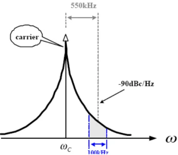
Fig.1.6.1 Conversion of noise around integer multiples of the oscillation frequency into phase noise………11
Fig.1.6.2 Illustration of phase noise specification………12
Fig. 1.1.1 Model of the ideal LC-resonant oscillato……….14
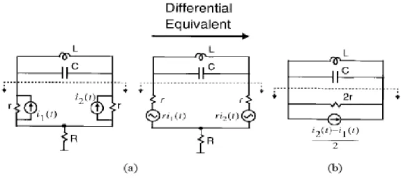
Fig. 2.1.1 (a) Current flow when the stage is switched to one side. (b) Differential equivalent circuit………15
Fig. 2.1.2 Simulated voltages and currents in the current-limited regime………..….16
Fig.2.1.3 Simulated voltages and currents in the voltage-limited regime………17
Fig 2.1.4 simulated tank voltage amplitude versus tail-current for the complementary differential oscillator………18
Fig. 2.1.5 Complementary LC oscillator with noise sources………19
Fig. 2.1.6 (a) Simplified model for transistor noise sources. (b) Differential equivalent circuit………..20
Fig.2.1.8. the simulated ISF’s of different noise sources in the 1.8-GHz complementary differential oscillator………...22
Fig.2.1.9. Evolution of tail noise current………...….23
Fig. 2.1.10 Induced sideband due to sinusoidal at Fdev and 2fo+Fdev……….23
Fig. 1.1.11 Two interleaved VCO configuration………...24
Fig. 2..2.1 (a) conventional quadrature vco with constant bias current (b) The waveform conventional quadrature vco(c) The phase noise of the conventional quadrature vco………..27
Fig.2.2.2. (a) QVCO with the biasing transistors switched by its own output (b) the simulated waveform of QVCO (C) The phase noise of QVCO………...29 Fig.2.2.3. (a) QVCO with the biasing transistors switched by its own output (b) QVCO with
Fig.2.3.1 Proposed SIPC-QVCO with CMOS schematic………..…32
Fig. 2.3.2 Block diagram of (a) the conventional P-QVCO and (b) SIPC-QVCO…..34
Fig. 2.3.3 Switching and coupling transistors and the LC-tanks for (a) The conventional P-QVCO and (b)The SIPC-QVCO………...34
Fig.2.3.4. (a) Simulated phase noise performances of the SIPC-QVCO. (b) Simulated phase noise performances of the P-QVCO...……35
Fig.2.3.5. (a) simulated time-domain outputs of SIPC-QVCO.(b) simulated time-domain outputs of P-QVCO………..….37
Fig.2.3.6. simulated time-domain outputs of too small coupling mos (sipc-qvco)…..38
Fig. 2.4.1 (a) The source injection parallel circuit by capacitance QVCO(b) The phase noise of sipc-qvco with capacitance. ………...40
Fig. 2.4.2 Quadrature output……….….43
Fig. 2.4.3 current waveform of Ic, Id, Itial……….….43
Fig. 2.5.1 Chip micrograph……….…....44
Fig. 2.5.2 Measurement instruments (a) Agilent E5052A signal source analyzer (b) HP 8563E spectrum analyzer (c) HP E3611A powesupply………...45
Fig 2.5.1 the phase noise of the proposed QVCO……….…..47
Fig 2.5.2 the power spectrum of the proposed QVCO………47
CONTENTS
Chinese Abstract II
English Abstract III
Acknowledgement IV
List of Figures V
Contents VII
Chapter 1 . introduction ...1
1.1 Introduction... 1 1.2 Oscillator Theory ... 2 1.3 Resonatorless VCO’s ... 4 1.4 LC-Tank VCO... 5 1.5 The Definitions of Q ... 71.6 The Origin of Phase Noise... 10
Chapter 2...13
Design and Implementation LC-Tank VCO’s ...13
2.1 Design issues in CMOSs differential lc oscillator ... 13
2.2 Design circuit for tail current of the oscillator... 26
2.3 Source injection parallel circuit (sipc) with MOS ... 32
2.4 . SIPC with capacitance ... 39
2.5 Measurement considerations... 44
2.6 Measurement results and comparison ... 46
Chapter 3 Conclusions and Future Work ...48
3.1 Conclusions... 48
Chapter 1 . introduction
Serving to give the outputs of frequency synthesizers, voltage-controlled oscillators (VCO’s) in fact determine the intrinsic output phase noise and thus necessitate careful designs. The design of VCO's becomes even more challenging in RF applications, where stringent requirements of phase noise and power consumption remain as the toughest tasks that RF IC engineers have to deal with.
1.1
Introduction
The VCO is, without a doubt, the most important block of the frequency synthesizer because it works at the highest frequency and requires a low phase noise. It is the element in frequency synthesizers that determines its overall quality. Up to now, VCO’s are one of the remaining building blocks that are difficult to integrate into a single chip transceiver, and large research efforts are put into the task of a complete integration of RF oscillators. Some of the most important specifications of a VCO are
Phase Stability: the frequency spectrum of a VCO output should look likes an ideal impulse, i.e., the phase noise of a VCO must be as low as possible. Electrical Tuning Range: the tunable frequency range of a VCO must be able to
cover the entire required frequency range of the interested application.
Tuning Linearity: an ideal VCO has a constant gain at the entire frequency range. Also, a constant VCO gain can simplifies the design procedure of VCO
Besides, the other characteristics including such as the output frequency stability with temperature, power consumption, and the cost of fabrication are also major concerns for all communication products.
Based on the considerations stated above, modern communication systems usually utilize LC-tank oscillators. Although some types of oscillators such as relaxation oscillators, ring oscillators, etc., implemented in advanced submicron CMOS technology may be also capable of achieving gigahertz operation frequency nowadays, their phase noise behavior and frequency stability at high frequency are
still not good enough for communication applications. LC-tank oscillators are the only type of integrated oscillator that will be capable of achieving the required high frequency and low noise at reasonable power consumption. In this chapter, we will first introduce the oscillator theory of an oscillator.
1.2
Oscillator Theory
Before presenting the various types of VCO's, it is necessary to review the basic concepts of oscillation. An oscillator generates a periodic output. As such, the circuit must entail a self-sustaining mechanism that allows its own noise to grow and eventually become a periodic signal. Most RF oscillators can be viewed as a feedback circuit. Consider the simple linear feedback system depicted in Figure 1.2.1(a), with the over all transfer function
( )
( )
H( )
S s H s X s Y − = 1 ) ( 1.1A self-sustaining mechanism arises at the frequency s0 if H(s0 ) = +1, and the oscillation
amplitude remains constant if s0 is purely imaginary, i.e., H(s0 = jw0 ) = +1. Thus, for
steady oscillation, two conditions must be simultaneously met at w0
(1) The loop gain, |H (jw0)|, must be equal to unity, and
Figure 1.2.1 (a) Feedback oscillatory system, and (b) addition of frequency-selective network to (a)
It’s the well-known Barkhausen’s criteria, the above conditions imply that any feedback system can oscillate if its loop gain and phase shift are chosen properly. Ring oscillators and phase shift oscillators are examples. However, in most RF oscillators, a frequency-selective network is included in the loop to stabilize the frequency, as shown in Figure 1.2.1(b). The frequency selective network is often referred as a “resonator”, and thus those oscillators without frequency selective network are referred as “resonatorless oscillators”. In most practical cases, a unity gain at oscillation frequency doesn't guarantee sustained oscillation and a gain greater than unity at oscillation frequency is required to ensure oscillation. Although a gain greater than unity leads to a growing oscillatory transient response rather than a sustained oscillation with constant amplitude, the increasing envelope of signal nevertheless saturates the circuit in some ways and the loop gain is degraded to unity.
We should also note that the Barkhausen’s criteria are necessary but not sufficient, even with the loop gain set to be higher than unity. For example, the phase shift around the loop may equal to 360 at zero frequency and the loop gain is sufficient, the circuit latches up rather than oscillates, since a signal of zero frequency with growing amplitude means nothing but a growing and eventually saturating dc signal . Also, when the circuit inhibits more than one frequency that has zero phase shift, the poles of interest may go through the imaginary axis more than once, which implies that at certain condition increasing gain actually stabilizes the loop by forcing the poles back to LHP (left-half plane). This is illustrated in with the Pierce oscillator as an example.
1.3
Resonatorless VCO’s
The Barkhausen’s criteria for oscillation can be met without resonators in a circuit as well. If the open- loop circuit exhibits sufficient gain at zero-phase frequency,oscillation occurs. Also, if the open- loop input/output characteristic entails hysteresis, the circuit may oscillate even if the small signal phase shift does not appear to besufficient
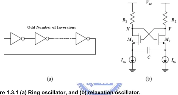
Figure 1.3.1 (a) Ring oscillator, and (b) relaxation oscillator.
An example of the first type is ring oscillator. As shown in Figure 1.3.1(a), if a cascade of M gain stages with an odd number of inversions is placed in a feedback loop, the circuit oscillates with a period equal to 2MTd, where Td is the delay of each stage with a fan-out of one. The oscillation can be viewed as occurring at the frequency for which the total phase shift is zero and the loop gain is unity. Va rious implementations of the gain stages utilized in ring oscillators along with methods of tuning the frequency are described in my reference.
Figure 1.2.1(b) shows an example of oscillators incorporating hysteresis. Called a “relaxation oscillator”, the circuit can oscillate even if C is the only storage element, simply because the positive feedback around M1 and M2 provides rapid switching at the end of each cycle, breaking the feedback loop for most of the period. At high frequencies, however, the hysteresis diminishes and oscillation occurs only if the poles at nodes X and
impedance seen looking into the X-Y port of the cross coupled pair is approximately equal to s
c
g
m 1 1 2 −− , that is, a negative resistance in series with a negative capacitance.
In high frequency operation, the first component cancels the loss in R1 and R2, and the second resonates with the capacitance at X and Y.
Resonatorless oscillators have not been popular in RF designs. This is becausethey not only exhibit an open- loop Q close to unity but also contain many noisy activeand passive devices in the signal path. For example, in a three-stage differential ringoscillator, the open-loop Q is approximately equal to 1.3, and nine transistors (including the tail current sources) and six load resistors add noise to the carries .
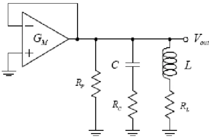
Figure 1.3.2 An LC-tuned oscillator as a feedback circuit.
1.4
LC
-Tank VCO
An LC-tank oscillator is a feedback network with an LC-tank as the feedback circuit. As stated before, oscillation occurs at the frequency at which the loop transfer function is one and has zero phase shifts. In reality, the loop transfer function is always designed to have value greater than one, but have zero phase shifts at the oscillating frequency. The amplitude of oscillation is usually limited by nonlinear effects. For the LC-tank oscillator shown in Figure 1.3.2, the oscillation conditions are already as Equation 1.2 to 1.4.
LC
O1
=
ω
1.2(
C
)
R
R
R
R
o
P L C effω
21
+
+
=
1.3(
C
)
R
G
M effω
o
2=
1.4From Equation 1.4, if we increase the value of C, the power consumption of the VCO increases, but the action improves the tuning range. The major criterion of an oscillator is to have a good phase noise performance. Phase Noise is important in our application because it determines the sensitivity of the receiver and the purity of the transmitter. Moreover, the inherent phase noise of the VCO dominates the noise performance of a synthesizer in that if the VCO phase noise degrades to a certain degree, the closed-loop couldn’t help improving output phase noise anymore. Hence, although the general idea of phase noise is already introduced in section 2.1, it is mandatory to restate the phase noise in this section in detail. The following discussions will begin with various definitions of quality factor Q since it has a great concern with the phase noise. Then the origin of phase noise will be discussed. Finally, some examples of phase noise requirements will be given.
1.5
The Definitions of Q
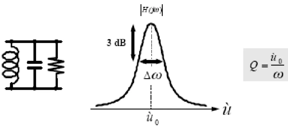
Figure 1.5.1 Definition of Q with two-sided –3dB bandwidth.
The quality factor Q is conventionally defined within the context of a second-order system with damped oscillatory behavior. As shown in Figure 1.5.1, a typical RLC tank has an impedance value as a function of frequency
( )
⎥ ⎥ ⎦ ⎤ ⎢ ⎢ ⎣ ⎡ − + = u u jQ R u j Zu
u
O o & & &&
&
1 1.5 With the quality factor Q and the oscillation frequency ω0LC and L C R Q=
u
&
O = 1 1.6The Q defined by the values of R, L and C here is derived from direct computation of impedance response and thus exhibits no physical meaning. Normalize the impedance response to its peak value R
( )
⎥ ⎥ ⎦ ⎤ ⎢ ⎢ ⎣ ⎡ − + = u u jQ u j Hu
u
O o & & &&
&
1 1 1.7Then the two-sided -3dB bandwidth Δω can be derived from evaluating the non-negative solutions of
1
0 0±
=
⎟
⎟
⎠
⎞
⎜
⎜
⎝
⎛
−
u
u
Q
u
u
&
&
&
&
1.8 which are⎥
⎥
⎥
⎥
⎦
⎤
⎢
⎢
⎢
⎢
⎣
⎡
⋅
+
+
=
⎟⎟
⎠
⎞
⎜⎜
⎝
⎛
+u
Q
u
u
u
&
Q
&
&
&
20 2 00
4
2
1
1.9⎥
⎥
⎥
⎥
⎦
⎤
⎢
⎢
⎢
⎢
⎣
⎡
⋅
+
+
−
=
⎟⎟
⎠
⎞
⎜⎜
⎝
⎛
−u
Q
u
u
u
&
Q
&
&
&
20 2 00
4
2
1
Q
u
A
&&
&
=
u
&
+−
u
&
−=
u
&
0 1.10
It is obvious that Q can be re-defined as the ratio between the oscillation frequency and the two-sided -3dB bandwidth
u A Q
u
O & &&&
= 1.11The definition in Equation 1.11 describes how "sharp" the transfer function of the RLC tank is, and hence how "pure" the oscillation output will be. However, if the inductor is removed, this definition can no longer be applied since there won't be such a band-pass response. A more general definition is the ratio of the stored energy and the dissipated energy per cycle
) ( ) ( n dissipatio Energy stored Energy Q= 1.12
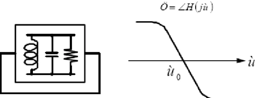
Note that this definition yields the same result as that given by the definition of Equation 1.11 for a simple RLC tank. Another definition proves especially useful in oscillators. Here the circuit is considered as a feedback system and the phase of the open- loop transfer function, f(w), is examined at resonance. To see how it works, first, the phase response f(w) can be derived from Equation 1.8
⎥ ⎥ ⎦ ⎤ ⎢ ⎢ ⎣ ⎡ ⎟ ⎟ ⎠ ⎞ ⎜ ⎜ ⎝ ⎛ − − = ∠ = − u u Q u j H
u
u
o & & &&
&
0 1tan
) ( φ 1.13which starts at low frequencies with a value of +90° and ends at high frequencies with a value of −90°, as shown in Figure 1.4.1. Take the derivative with respect to w and evaluate the result at w = w0
u
u
u
u
u
u
u
u
Q
O O O u Q Q o o u u d dO
&
&
&
&
&
&
&
& & & 2 1 1 1 2 2 2|
= ⎥ ⎥ ⎦ ⎤ ⎢ ⎢ ⎣ ⎡ + + − =⎥
⎦
⎤
⎢
⎣
⎡
−
= φ 1.14Herein we see that the quality factor Q can be alternatively defined as
u d d Q
u
&&
φ 2 0 = , 1.15Evaluated at w = w0. Called the "open-loop Q", this definition provides an interesting point
of view that if the frequency slightly deviates from the oscillation frequency
ω
0, the phase will deviate from 0 ndicated in the Barkhausen criteria as the condition of oscillation. The degree the phase deviates from 0 depends on the slope,ω φ
d d
, of the transition in the phase response. If the slope, and hence the Q, is large, small deviation in
frequency causes the phase to drift far away from the condition of oscillation, and thus the loop will force the frequency back to where the phase most meets Barkhausen’s criteria. In other words, the open-loop Q is a measurement of how much the closed-loop system opposes variations in the frequency of oscillation.
Figure 1.5.2Definition of Q based on open-loop phase slope.
1.6
The Origin of Phase Noise
In the section 2.1.1, we analyze noise source from the circuit and we describe effects of noise now.It is possible to analyze phase noise either in the time domain or in the frequency domain. Both analyses are equivalent due to the duality between the time and frequency domains. For ring oscillators, people would like to use a time domain analysis. Hence, the notion of phase noise is translated into “jitter”. The jitter can be expressed as the time difference between the zero crossing of the real oscillator and an ideal oscillator oscillating at the same average frequency. It is common to represent the jitter in a histogram. The specification that people usually report under the name of jitter is in fact the variance of the jitter since the jitter itself is different for each cycle. Indeed, for ring oscillators, the frequency of oscillation is not as obvious as for LC-tank oscillators. Besides, people like to refer to ring oscillators as delay cells, which implies a time constant rather than a frequency.
Figure1.6.1Conversion of noise around integer multiples of the oscillation frequency into phase noise
However, for LC-tank oscillators, since an oscillator is a periodically time varying system. The time-varying nature of the VCO converts the noise around integer multiples of the oscillating frequency into phase noise, which is illustrated in Figure 1.5.1. The major noise sources are noise generated in transistors in the GM cell shown in Figure 1.3.2 and the thermal noise by various resistances in circuit. A detail analysis on the effect of various noise sources is shown in my reference. The noise generated by a transistor is shown in Equation 1.16. Due to the hot carrier effect, the value of a in Equation 1.16 can be as high as three in short channel devices, while a is around 2/3 for long channel devices. gd0 is the channel conductance and is defined as the reciprocal of the resistance at the drain node when Vds=0. gd0 is a function of W, L, and Vgs.
f
K
KT
f
I
g
i
B a d noise=
0+
Δ
24
γ
1.16To improve the phase noise, we should increase the ratio of the carrier power to the noise power. One way to do it is to increase the size of the transistors and reduce the biasing current. Keeping gd0 constant, the thermal noise generated by the transistors is
kept at a constant level, but the 1/f noise reduces due to the increase in the total gate area. However, increasing the gate dimension, the gate capacitance contributes a larger portion of the total capacitance required for oscillation, and hence reducing the tuning range. Another noise source is the thermal noise of the series resistance of the inductors. The noise generated by the resistor is
KTR
v
noise4
2
=
1.17To minimize the noise power generated by the series resistance, the quality factor of the inductor should be maximized.
Chapter 2
Design and Implementation LC-Tank VCO’s
2.1
Design issues in CMOSs differential lc oscillator
An analysis of phase noise in differential crosscoupled inductance–capacitance (LC) oscillators is presented. The effect of tail current and tank power dissipation on the voltage amplitude is shown. In this section, I will consider about the effect of tail current and tank power dissipation. Various noise sources in the complementary cross-coupled pair are identified, and their effect on phase noise is analyzed. The predictions are in good agreement with measure- ments over a large range of tail currents and supply voltages.
Due to their relatively good phase noise, ease of implementation, and differential operation, cross-coupled inductance–capacitance (LC) oscillators play an important role in high-frequency circuit design. In this paper, the time-variant phase-noise model of my reference will be applied to analyze these oscillators. A simple expression for the tank amplitude is first obtained. The effect of different noise sources in such oscillators is then investigated, and methods for exploiting the cyclostationary properties of noise are shown. New design implications arising from this approach and experimental results are given.
The dependence of tank amplitude on the tail current and supply voltage is calculated in Section I. The effect of noise sources in both active and resistive tank loss is analyzed in Section. Section C is to investigate the effect of tail-current noise.
I. TANK MPLITUDE
The model of LC-resonant oscillators is shown in fig2.1.1. The oscillation frequency is decided by the equivalent inductance Leq and capacitance Ceq in the tank. For the purpose of
frequency tuning, it is common to use varactors and to vary Ceq in LC-resonant oscillators. The
tuning range has to be very wide to meet the UWB system specification. Unfortunately the noise on the control voltage translates into phase noise and wider tuning range makes this problem more serious. Moreover, the size of the varactors has to be increased and the nonlinearity of larger varactors converts more amplitude noise into phase noise.
Fig. 0.1.1 Model of the ideal LC-resonant oscillator
This VCO adopts a complementary cross-coupled negative-gm configuration which has several benefits: (1) only one inductor is needed and large chip area is saved. (2) Smaller voltage drop across the MOS transistors reduces the effect of velocity saturation in the short channel regime. (3) The complementary structure offers higher trans-conductance for a given current, which results in fast switching of the cross-coupled pair. (4) The output swing is more symmetry to alleviate the noise up-conversion effect and then phase noise performance is improved. In addition, the current source is in parallel with a capacitor which provides a path to remove the noise disturbance from the current source. For symmetry the capacitor is actually placed at both sides of the current source.
Tank voltage amplitude has an important effect on the phase noise, as emphasized by the presence of q in the denominator of the expression for the single-sideband phase noise
( )
⎟
⎟
⎟
⎟
⎟
⎠
⎞
⎜
⎜
⎜
⎜
⎜
⎝
⎛
Δ
Δ
•
=
Δ
Γ
ω
ω
2 2 2 max 22
log
10
RMS nq
i
f
L
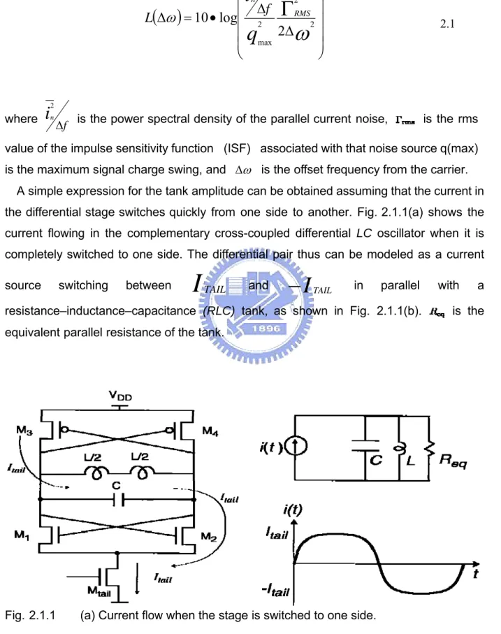
2.1 wherei
n f Δ 2is the power spectral density of the parallel current noise, is the rms value of the impulse sensitivity function (ISF) associated with that noise source q(max) is the maximum signal charge swing, and Δ is the offset frequency from the carrier. ω
A simple expression for the tank amplitude can be obtained assuming that the current in the differential stage switches quickly from one side to another. Fig. 2.1.1(a) shows the current flowing in the complementary cross-coupled differential LC oscillator when it is completely switched to one side. The differential pair thus can be modeled as a current source switching between
I
TAIL and−
I
TAIL in parallel with a resistance–inductance–capacitance (RLC) tank, as shown in Fig. 2.1.1(b). is the equivalent parallel resistance of the tank.
(b) Differential equivalent circuit.
At the frequency of resonance, the admittances of the L and C cancel, leaving Req Harmonics of the input current are strongly attenuated by the LC tank, leaving the fundamental of the input current to induce a differential voltage swing of amplitude
R
I
tail eq π4 across the tank if one assumes a rectangular current waveform. At high frequencies, the current waveform may be approximated more closely by a sinusoid due to finite switching time and limited gain. In such cases, the tank amplitude can be better approximated as
V
tank≈
I
tailR
eq 2.2 This mode of operation is referred to as the current-limited regime of operation since, inthis regime; the tank amplitude is solely determined by the tail-current source and the tank equivalent resistance. Fig. 2.1.1 shows the simulated node voltages as well as the drain currents of the NMOS transistors, M1 and M2 in this regime of operation. The values of L and are such that the circuit oscillates at 10GHz.
Fig. 2.1.2 Simulated voltages and currents in the current-limited regime
Fig.2.1.3 Simulated voltages and currents in the voltage-limited regime
Note that (2) loses its validity as the amplitude approaches the supply voltage because both NMOS and PMOS pairs will enter the triode region at the peaks of the voltage. Also
the tail NMOS transistor may spend most (or even all) of its time in the linear region. This behavior can be seen in the simulated voltages and currents shown in Fig.2.1.3 The tank voltage will be clipped at Vdd by the PMOS transistors and at ground by the NMOS transistors. Therefore, for the oscillator of Fig.2.1.1 (a), the tank voltage amplitude does not significantly exceed vdd Note that since the tail transistor is in the triode region, the tail current does not stay constant. Thus, the drain-source voltage of the differential NMOS transistors can drop significantly, resulting In a large drop in their drain current, as shown in Fig. 2.1.3. This region of operation is known as the voltage-limited regime.
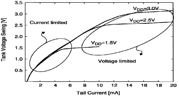
Fig.2.1.4 shows the simulated tank voltage amplitude as a function of tail current for three different values of vdd. As can be seen, the tank amplitude is proportional to the tail current in the current-limited region, while it is limited by Vdd in the voltage-limited regime.
Fig. 2.1.4 Simulated tank voltage amplitude versus tail-current source for the complementary differential oscillator.
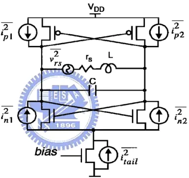
II. NOISE SOURCES FROM CMOS
Fig. 2.1.5 depicts the noise sources in the oscillator. The noise power densities for these sources are required to calculate the phase noise using (1). In general, these noise sources are cyclostationary because of the periodic changes in currents and voltages of the active devices. In this section, we first introduce a simplified stationary model for the noise sources and then examine subtleties arising from their cyclostationary behavior. It is very useful to analyze phase noise of the circuits in the section 2.2, 2.3 and 2.4.
Fig. 2.1.6 (a) Simplified model for transistor noise sources. (b) Differential equivalent circuit.
In a simplified stationary approach, the power densities of the noise sources can be evaluated at the most sensitive time (i.e., the zero crossing of the differential tank voltage) to estimate the effect of these sources [7]. Fig. 2.1.6(a) shows a simplified model of the sources in this balanced case. Converting the current sources to their Thevenin equivalent and writing Kirchoff’s voltage law, one obtains the equivalent differential circuit shown in Fig. 2.1.6(b). Note that the equivalent parallel resistance is canceled by the negative resistance provided by the positive feedback. Therefore, the total differential noise power due to the four cross-coupled transistors is
⎟ ⎠ ⎞ ⎜ ⎝ ⎛ + = ⎟ ⎠ ⎞ ⎜ ⎝ ⎛ + + + =
i
i
i
i
i
i
i
cc n n p p n p 2 2 2 1 2 2 2 2 4 1 2 2 1 2 1 Wherei
i
i
n n n 2 2 2 1 1= = andi
i
i
p p p 2 2 2 1 1= = Noise densities fi
n Δ 2 and fi
p Δ 2 are given by(
V
V
)
C
i
T GS OX n L W kT f = − Δ 4 γμ 2Where μ is the mobility of the carriers in the channel, Cox is the oxide capacitance per unit area, W and L are the width and length of the MOS transistor, respectively,
V
GS is the gate- source voltage, andV
T is the threshold voltage. Equation (4) is valid for both short- and long-channel regimes of operation. However, is around 2/3 for long-channel transistors while it may be between two and three in the short-channel region due to hot-electron effects?In addition to these sources, the contribution of the effective series resistance of the inductor
r
s caused by ohmic losses in the metal and substrate is given byR
r
i
P S rs C kT L kT f 4 4 2 = = Δ Where(
)
r
L
r
Q
R
s s P oω
2 2 =≈ is the equivalent parallel resistance at the frequency of oscillatio.
III TAIL CURRENT NOISE SOURCE
To gain further insight into the effect of the tail noise source, its ISF, as well as those for the NMOS and PMOS drain noise sources, are shown in Fig. 2.1.8. The ISF’s are calculated using direct impulse injection and measuring the resultant phase shift.
As can be seen from Fig. 2.1.8, the ISF associated with the tail-current source has a fundamental frequency that is double the oscillation frequency. This is expected since the tail nodeis pulled up every time each one of the differential NMOS transistors turns on, and thus the tail node moves at twice the frequency of the differential voltage.
Fig.2.1.8. The simulated ISF’s of different noise sources in the 1.8-GHz complementary differential oscillator.
Due to this frequency doubling, the Fourier component of the ISF at
ω
odenoted by C1 is zero, and therefore the noise of the tail-current source in the vicinity ofω
ohas no effect on the differential noise current. However, even-order coefficients such asc
0,c
2, andc
4are significant; therefore, noise components around even harmonics ofω
o have a significant effect on the phase noise, as shown in Fig.2.1.9. Also, the low-frequency noise component of the tail noise source can affect phase noise through asymmetry. To verify this behavior, a sinusoidal current with amplitude of 200μA was injected in parallel with the tail-current source, and the induced sideband power below the carrier was measured using fast Fourier transform (FFT) analysis in HSPICE. In Fig. 2.1.10, sinusoidal injection at low frequencyf
mand in the vicinity of twice the oscillation frequency
f
f
m
+
2
0 results in noticeable sidebands. However, sinusoidal injection of the same amplitude atf
f
m
+
0 does not produce any observable
sidebands.
Fig.2.1.9.Evolution of tail noise current
The tail capacitor mentioned in the previous section attenuates the high-frequency noise components of the tail-current source, so one expects corresponding attenuation of phase noise due to this noise. In fact, the induced sidebands due to injection at
f f + m
2 0 in the presence of the 10-pF tail capacitor are very small and are below the
numerical noise floor of the FFT operation.
Since upconversion of 1/f noise is thus the most significant remaining noise component of noisy tail current, one must properly size the tail-current transistor and satisfy the single-ended symmetry criterion by sizing the cross-coupled NMOS and PMOS transistors properly.
How to obtain quadrature signals
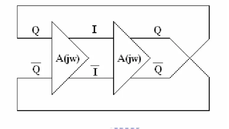
There are several ways to obtain quadrature signals: divider-by-2 circuit, RC poly-phase filters, and two interleaved voltage-controlled oscillators. The divider-by-2 circuit needs an oscillator operating at 2 times higher than the desired frequency and a high-speed frequency divider. Both circuits dissipate a lot of power in spite of a smaller chip size. RC poly-phase filters attenuate the signal and increase the effective capacitance of the tank. Also a lot of chip area is needed for a good matching of the filters. For the low power consumption and quadrature phase accuracy, two interleaved voltage-controlled oscillators are adopted in this circuit. According to the Barkhausen criterion, oscillation occurs only when the loop gain [A(jω)]4 is unity. Therefore A(jω) has amplitude of one with a 90 degree phase shift and quadrature signals are obtained at the four outputs of these two VCOs.
Fig. 0.1.11 Two interleaved VCO configuration
As shown in Fig. 0.1.12 (a), the VCO is in a complementary cross-coupled negative-gm configuration. The advantages of this configuration are mentioned in Chapter 2. However, there is a difference from the VCO in Chapter 2. The tail current source is removed to maximize the output swing. Two benefits also achieved thanks to the removal of the current source. First the current source is the main contributor to the phase noise. Second, when all transistors in the VCO core are put in GHz-switching bias condition, flicker noise will apparently be reduced by about 10 dB. The dimension of four cross-coupling PMOS transistors is an important parameter. If cross-coupling is made weak, two-tones oscillation exists probably; if it is made strong, DC power is wasted and more capacitance is added into the LC-tank. By means of transient simulations, the optimal width of the cross-coupling
transistors should be set to one-third of the width of the core transistors while the length of all transistors is chosen as the minimal length (0.18 μm in this circuit)
2.2
Design circuit for tail current of the oscillator
A 10-GHz CMOS conventional quadrature voltage controlled oscillator (QVCO) is described by fig.2.1.2 Two differential pairs (one for negative gm generation and the other one for the coupling input) of each resonator have separate biasing transistors which are switched on and off by the coupling input of each resonator. The simulation of proposed VCO in fig2.2.2 implemented in a 0.18-μm CMOS technology shows 5-dB phase noise improvement from a conventional QVCO with constant tail current sources while the two QVCOs consume the same power of 3.88 mW in the simulation.
With quadrature voltage controlled oscillator (QVCO) where two LC-tank VCOs coupled with each other as shown in Fig. 2.2.1, accurate quadrature-phase local oscillator (LO) signals can be obtained. The conventional QVCO in Fig.2.2.1, however, usually shows poorer phase noise performance than a single-phase VCO. This is because the phase shift of the resonator of the QVCO is not zero at the oscillation condition and thus its quality factor is degraded .
Several approaches have been reported to improve the phase noise performance of QVCO. In [1] and [2], additional phase shift was inserted between the two LC-tanks, allowing each resonator to be optimally driven at zero-degree phase shift. In this way, superior phase noise performance was obtained but the accurate control of the phase shift is complicated and the phase shifter introduces additional power consumption. As alternative ways, the series coupling and harmonic coupling schemes are developed which requires either a higher supply voltage or an on-chip transformer.
In this section, the phase noise of a QVCO is improved by the newly proposed coupling and biasing scheme in fig2.2.2. In the following, the detailed description of
the proposed low-phase noise QVCO and the simulated results of the 10-GHz QVCO implemented in a 0.18-μm CMOS technology are given
One of the major sources of the phase noise of MOSFET VCO is the noise of biasing transistor. For a single-phase CMOS VCO, it has been shown the phase noise can be greatly reduced if biasing transistor is switched on and off because the trapped electrons causing the noise are released periodically . This switched biasing scheme can be extended to QVCO by the output voltage as shown in Fig. 2.2.2(a). According to the SpectreRF simulation result shown in Fig.2.2.2, the phase noise is improved by 5dB from the conventional QVCO in Fig.2.1.1.
(a)
(b)
(c)
Fig. 2.2.1 (a) conventional quadrature vco with constant bias current (b) The waveform conventional quadrature vco
For the conventional QVCO in Fig. 2.1.1(a), however, the output swing is limited by the common-source node voltage because the minima of the output are not aligned with the minima of the common-source node voltage as shown in Fig. 2.1.1(b). This is due to the time delay caused by the resistance of the transistor in the triode region and the parasitic capacitance at the common source node.
(a)
(c)
Fig.2.2.2. (a) QVCO with the biasing transistors switched by its own output (b) The simulated waveform of QVCO
(C) The phase noise of QVCO
In this work, the special circuit shown as fig2.2.2(a) in stead of providing a fixed tail current, two tail transistors separated , which are controlled by the differential output voltage, are employed. Since the tail transistors are turn off alternatively by the differential output of the VCO during each oscillating period, the probability of trapping carriers by the dangling bonds in the conducted channels is significantly reduced. For the 10-GHz VCO design, simulation results indicate that a 5-dB phase noise improvement at 1-MHz offset can be achieved by employing the switched-bias technique.
In fact, the mos as tail current source can not seen as the ideal switches, because output voltage swing is not enough big to turn on and off all time. In the fig 2.2.2, it shows this way for current source of the signal vco design is not good way, but this way could improve much when the circuit becomes qvco. We will discuss this issue of qvco in the next section.
(a)
(b)
Fig.2.2.3. (a) QVCO with the biasing transistors switched by its own output (b) QVCO with the constant tail current source.
2.3
Source injection parallel circuit (sipc) with MOS
This scction presents a source-injection parallel coupled (SIPC) quadrature voltage-controlled oscillator (QVCO) topology. In the proposed SIPC-QVCO, compare to the conventional parallel-coupled LC-QVCO (P-QVCO), the coupling transistors are configured in a way so that the noise, con- tributed by the coupling transistors at the output, can be avoided. The newly proposed SIPC-QVCO and conventional P-QVCO are fabricated based on 0.18μm CMOS technology. The phase noise of SIPC-QVCO simulated at 10GHz shows more than 10 dB improvements than that of the conventional P-QVCO over the offset frequency range of 1 MHz while dissipating the same amount of power.
THE QUADRATURE LO signal is a key element in many of the direct conversion transceivers whic tend to dominate today’s wireless communication technology. ince the introduction of the parallel-coupled LC-quadrature voltage-controlled oscillator (QVCO) (P-QVCO) topology, which was proposed by Rofougaran [1], it has become one of the most commonly used topology for the quadrature signal generation. Recently, Andreani [2] reported a series-coupled LC-QVCO topology (S-QVCO) that exhibits improvement in phase noise compare to the P-QVCO. However, the S-QVCO has disadvantage in the low supply voltage application, which is one of the major trends in concurrent technologies, due to the stack of the coupling transistors in series with the cross-coupled transistors of the differential VCO. In this letter, a source-in- jection parallel-coupled LC-QVCO (SIPC-QVCO) topology is proposed as a low voltage and low phase noise QVCO.
A.SIPC-QVCO Topology Description
Fig.2.3.1cshows the schematic of the proposed SIPC-QVCO topology.As shown in Fig.2.3.1, the SIPC-QVCO consists of two LC-tuned differential VCOs and four coupling transistors. Note that, contrary to the conventional P-QVCO, the drain nodes of the coupling transistors are connected directly to the supply voltage ( ). In
VDD VDD Vctrl Vbias Vbias VDD VDD Vctrl Vbias Vbias
Fig.2.3.1 Proposed SIPC-QVCO with CMOS schematic.
B. Mechanism of Quadrature Signal Generation
The schematic of the SIPC-QVCO might seem like a minor modification from the conventional P-QVCO. However, the mechanism for quadrature signal generation is fundamen- tally modified. Fig. 2.3.2(a) and (b) represent the P-QVCO and SIPC-QVCO as a combination of functional block diagrams. As can be seen in Fig.2.3.2(a), the quadrature output signals in P-QVCO are generated by the combination of two differ- ential-VCOs and the cascade of two differential amplifiers (Implemented as coupling transistors) with one of them incross-connection. In Fig. 2(b), the simplified block diagram of the SIPC-QVCO is constructed as an alternating combination of two differential-VCOs and two frequency-doublers. The coupling transistor pairs and are configured as differential voltage buffer.
Fig. 2.3.2 Block diagram of (a) the conventional P-QVCO and (b) SIPC-QVCO
Fig. 2.3.3 Switching and coupling transistors and the LC-tanks for (a) the conventional P-QVCO and (b) the SIPC-QVCO.
C. Phase Noise Analysis
To understand the advantage of the SIPC-QVCO in phase noise, Fig.2.3.3 compares some parts SIPC-QVCO with P-QVCO: the switching and coupling transistors and the
transistors modeled as a voltage source in series with the gate and
i
n2
represents the resulting noise current in the drain. In the case of conventional P-QVCO shown in Fig. 2.3.3(a), when the coupling transistor is in saturation, the resulting 1/f noise current
i
n2 flows through the inductor L1. Since the inductor impedance at low frequencies is small, the voltage drop across the LC-tank byi
n2 is insignificant. However, when the coupling transistor turns off, the abrupt change in the noise current leads to a voltage induction across the inductor L1, in proportion to the value of and the time derivative, which could be a significant amount. Therefore, the switching operation of the coupling transistors effectively up-converts the 1/f noise to the frequency of oscillation leading to phase noise degradation. This is the main reason for the degradation of the inferior phase noise performance in P-QVCO compare to that of the core differential-VCO.In comparison, with the SIPC-QVCO, the 1/f noise of the coupling transistor contributes no voltage induction across the LC-tank since the drain of the coupling transistors are directly connected to the supply voltage as shown in Fig.2.3.3 (b).
Note that the separation of the coupling transistors from the LC-tuning circuits helps to obtain wider tuning range as parasitic capacitances of the coupling transistors are separated.
D.SIMULATION RESULT
The proposed SIPC-QVCO and the conventional P-QVCO have been implemented with a 0.18μm CMOS technology. For the fair comparison, both QVCOs adopted same active and passive component sizes and biased to dissipate the same total dc current of 16 mA from 1.5-V supply. Both QVCOs are simulated at the same frequency of 10 GHz by the small adjustments in the control voltage of the varactor. Fig. 2.3.4 compares the phase noise performance of the two QVCOs. As can be seen in Fig. 4, over the offset frequency ranges of 10KHZ ~ MHz, SIPC-QVCO shows more than 10-dB superior phase noise performance compare to that of the conventional P-QVCO. The simulated output power level of each quadrature signal was -10dBm. Fig.2.3.5 shows the simultadd time domain signal operating at 10 GHz.
(a)
(b)
Fig.2.3.4. (a) simulated phase noise performances of the SIPC-QVCO. (b) Simulated phase noise performances of the P-QVCO
(a)
(b)
Fig.2.3.5. (a) Simulated time-domain outputs of SIPC-QVCO. (b) Simulated time-domain outputs of P-QVCO
I have to be careful for designing size of mos( ). The size of mos() is too small that the two vco can not generate quadrature signal as shown in fig. 2.3.6. However, more large size of the coupling mos causes more power dissipation, because the drain
nodes of the coupling mos are connected directly to the supply voltage (vbias). In order to design low power qvco, I have to reduce the size of coupling mos in the SIPC-QVCO, so in the next section, we try to not use coupling mos to obtain quadrature signal.
2.4.
SIPC
with capacitance
A novel quadrature voltage controlled oscillator (QVCO) using source injection parallel coupling with the capacitances is presented. The QVCO realized with LC-tank is demonstrated in a 0.18um RF CMOS 1P6M process. Using the switch of current source technique efficiently reduces the power dissipation. However, by stacking switching transistors, the architecture cannot perform well in phase noise. Through an improved circuit schematic with source injection parallel coupling, the phase noise of the circuit can be lower than vco in the section 2.2. As a result of reducing four transistors in the circuit, the total power dissipation can be cut down even more by using four capacitances to coupling two vco cores. The simulation shows the phase noise is around -109dBc/Hz at 1MHz offset as shown in fig 2.4.1 and the output frequency tuning range of the fabricated QVCO is 1.8 GHz ranging from 9.15 to 10.95 GHz. The circuit draws only 1.8.mA from a 1.5-V supply. Compared with the recent works, the proposed topologies show a better phase noise performance and can be for low-power applications.
VDD VDD Vctrl VDD VDD Vctrl (a)
(b)
Fig. 2.4.1 (a) the source injection parallel circuit by capacitance QVCO (b) The phase noise of sipc-qvco with capacitance.
The development of single-chip CMOS solutions for the 10-GHz wireless local area network standard is desirable to enable implementations at low cost. In today’s complex radio architecture, it is often necessary for the local oscillator in a transceiver to produce two tones with a quadrature phase relationship. The voltage-controlled oscillator has been the subject of intense study. Recently, a CMOS VCO can be implemented by using a ring structure or an LC tank. Both of them are beneficial and detrimental. By definition, the ring VCO is known for a wide tuning range but drawback of a high phase noise that it is disqualified for most structures in modern RF transceivers. Accordingly, most investigations are focused on the LC VCO design. Owing to the limited range of the variable capacitance of the varactor, the tuning range of CMOS LC VCOs is very small. Hence, Razavi proposed that the varactor controlled by the DC potentials at both of its input terminals to enable the LC VCO yielding a wide tuning range. In recent years, several techniques exist to generate quadrature . Each method has its own advantages and disadvantages. Different implementations of quadrature oscillators can be found in the literature:
1) Using four-delay stage ring oscillator to fulfill the quadrature phase.
filter.
3) A VCO running at double frequency followed by a digital frequency divider based on flip-flop.
4) Two oscillators are injection locked in quadrature by coupling their second-order harmonic in anti-phase, and using a coupling network that exhibits high odd-mode and low even-mode impedance.
5) Two crossed-coupled VCO forced to run in quadrature by using coupling transistors and capacitance. In additional coupling transistors in parallel with the tank of two differential oscillators are used for quadrature generation (P-QVCO). Alternative solutions are the series-coupled QVCO (S-QVCO) topologies as proposed in fig 1.4.. That exhibits improvements in terms of phase robustness and phase noise compared to the P-QVCO. With the demand for low cost and high integration of wireless transceiver building blocks, here, we present an alternative method to obtain quadrature oscillator based on the switching current source in the triode region technique to reduce the power dissipation. In this work, the original coupling transistors are modified by using source injection parallel coupling to improve the phase noise. A new QVCO using switch current source technique and source injection parallel coupling is demonstrated here.
Circuit Blocks Description- Figure 2.4.1 shows the proposed QVCO topology. In
the section 2.2, the circuit of the tail current source proposed by fig 2.2 can not work as the two ideal switches, because the output voltage signal limited by the circuit is not enough big to turn off mos of current source. This VCO adopts a cross-coupled negative-gm configuration since the structure offers higher trans-conductance for a given current, which results in fast switching of the cross-coupled pair. The cross-coupled VCO and the current source operate as switches and the topology consists of two identical VCO in parallel. Each one is composed of two switching transistors as the current source, varactors Cv and inductors L. In order to analyze this circuit, the following introduction is divided into two parts: (1) the switching current source technique. (2) The source injection parallel coupling.
(1) the switching current source in the triode region of the technique
The main advantage of switching current source in the triode region of the technique is to lower the power dissipation, because the MOS biased by the
designed to control the two side of the varactors since the dc voltage are different between two differential output nodes (I/Q). By way of adding capacitors C for dc block and ac short, the voltage of the netX is different as shown fig 2.4.3. The circuit is equivalent for two identical VCO in ac and two VCO in parallel like . In general, a differential VCO uses a current source to bias oscillators reliably and the phase noise of the VCO is increased. The node Vx (Vy, Vz, Vw ) which are drain of tail current source is operated at the same frequency of the oscillation frequency of the LC tank VCO, the node VX( Vy, Vz, Vw )since the node is pulled up when each one of the differential NMOS turn on. As a result, the small capacitor C is adopted for ac short to inject the high-frequency from another vco core, then the mos work as switches. The noise of current source is reduced. A VCO with a current source in the triode region can operate with a low power supply and work as two ideal switches in the proposed QVCO.
The main issue for recent QVCO approach is to achieve a monolithic integration between low phase noise with a wide frequency tuning range and low power consumption at given operating frequencies. As mentioned above, power consumption can be decreased to a half compared to the conventional QVCO topologies and the phase noise can be decreased by this special way. Due to stacking switching transistors to provide current like the ideal switches, the architecture performs well in phase noise. Hence, the source injection parallel coupling will improve the phase noise, because the MOS of the current source is affected to work like the two ideal switches by another vco core
(2) The source injection parallel coupling
The use of source injection parallels removes the additional noise contributions compared to the conventional coupling transistor based topology, because there are no coupling MOS to add noise in the circuit. The coupling transistors are removed and the two differential VCOs are coupled through the source injection parallel. The capacitors C are adopted for ac coupling and dc block. Therefore, the source injection parallel coupling can be seen as the coupling transistors in the section 2.3. In the other hand, the conventional coupling transistors dissipate 30% ~ 100% of the power
and the power dissipation can be avoided altogether.
Fig. 2.4.2Quadrature output
2.5
Measurement considerations
All of the building blocks mentioned in previous sections will be combined to be a whole frequency synthesizer and simulated together. Fig. 2.5.1 shows the whole circuit schematic. The die size is roughly 0.61mm x 1.15mm.
The measuring equipment for this circuit contains Agilent E5052A signal source analyzer (Fig. 2.5.2(a), at CIC), HP 8563E spectrum analyzer (Fig. 2.5.2(b), at LAB), HP E3611A power supply (Fig. 2.5.2(c), at LAB).
(a)
(b)
(c)
Fig. 2.5.2 Measurement instruments
(a) Agilent E5052A signal source analyzer (b) HP 8563E spectrum analyzer (c) HP E3611A power supply
2.6
Measurement results and comparison
Measurement Result- Figure 2.6.1 shows the layout of the proposed QVCO
fabricated in TSMC 0.18 μm RF CMOS 1P6M process. The chip sizes are 0.61 x 1.115 mm2. According to Fig. 2.6.3, the output frequency tuning range of the fabricated QVCO is 1.3-GHz ranging from 9.1 GHz to 10.4 GHz from the center frequency of 10.09 GHz at Vctrl which is 1.5V. Fig.2.6.2 (a) shows the phase noise of -115.7dBc/Hz at 1MHz offset at frequency 10.38GHz. The core current consumed 2.48mA from a 1.5V supply. The figure-of merit (FOM) characteristic is expressed as
( )
⎥⎥⎥ ⎦ ⎤ ⎢ ⎢ ⎢ ⎣ ⎡ =⎟⎟
⎠
⎞
⎜⎜
⎝
⎛
Δ
f
P
f
ply L o FoM sup 2 1 log 10 λ 2.2Here, fo is the oscillation frequency of the VCO, fΔ is the offset frequency, and Psupply
is the power consumption. In order to compare with the recent published papers, the power-frequency-normalized figure of merit (FOM) is calculated. According to Table 1, the performance of the proposed QVCO is an excellent one for low-power topology compared with the reported results in the literature. FOM of the proposed QVCO is 190 db.
(b)
Fig 2.5.1 phase noise of the proposed QVCO
Fig 2.5.2 the power spectrum of the proposed QVCO.
Fig 2.5.3 the tuning rang of the proposed QVCO.
Chapter 3
Conclusions and Future Work
3.1 Conclusions
A low-power quadrature voltage-controlled oscillator using source injection parallel coupling (SIPC) technique and switching current source is demonstrated. This VCO adopts a cross-coupled negative-gm configuration since the structure offers higher trans-conductance for a given current, which results in fast switching of the cross-coupled pair. The advantage of switching current source technique can lower the power dissipation. Although power consumption can be decreased compared to the conventional QVCO topologies, it will increase the phase noise due to stacking switching transistors in series like a cascade. We also use the source injection coupling to improve the phase noise. Additionally, because of less coupling transistors used, the capacitance coupling can also lower the power dissipation. Based on measurement results, the power consumption of the core current is only 2.48mA. The measured phase noise, power consumption and carrier frequency is close to simulated.
Table 3-1 Comparison and Discussion
[1] Jong-Phil Hong, Seok-Ju Yun, Nam-Jin Oh, and Sang-Gug Lee,” A 2.2-mW Backgate Coupled LC Quadrature VCO With Current Reused Structure” IEEE MICROWAVE AND WIRELESS COMPONENTS LETTERS, VOL. 17, NO. 4, APRIL 2007
[2}Chan-Young Jeong, and Changsik Yoo,“5-GHz Low-Phase Noise CMOS
Quadrature VCO”, IEEE MICROWAVE AND WIRELESS COMPONENTS LETTERS, VOL. 16, NO. 11, NOVEMBR 2006
[3]Sangsoo Ko, Jeong-Geun Kim, Taeksang Song, Euisik Yoon, and Songcheol Hong, “K- and Q-Bands CMOS Frequency Sources With X-Band Quadrature VCO”, IEEE TRANSACTIONS ON MICROWAVE THEORY AND TECHNIQUES, VOL. 53, NO. 9, SEPTEMBER 2005
[4]Shenggao Li,Issy Kipnis,Mohammed Ismail,“A 10-GHz CMOS quadrature LC-VCO for multirate optical applications”,IEEE Journal of Solid-State Circuits, Octorber 2003.
-190.
3
-115.7
2.48
9.1~10.4
0.18
This
Work
-163
-95-
8
10
0.13
[4]
-188
-118
6.57
10.18~11
0.18
[3]
-184.
-117
5.5
0.13
[2]
-186.
-124
2.01
0.18
[1]
FO
M
Phase
Noise
[dBc/Hz]
Core
Current
[mA]
Frequen
cy
[GHz]
Technolo
gy
[um]
QVCO
Reference
[1] B. Razavi,“A 1.8V GHz CMOS voltage-controlled oscillator,” IEEE Int. Solid-State
Circuit Conf. (ISSC) Dig. Tech. Papers, San Francisco, CA, pp.388-389, Feb.1997.
[2] Wang, C. S., S. W. Kao and P. C. Huang, “A low phase noise wide tuning range CMOS quadrature VCO using cascade topology,” IEEE Asia-Pacific Conference on Advanced
System Integrated Circuits, pp. 138-141, August 2004
[3] Vancorenland, P. Steyaert, M.“A 1.57GHz fully integrated very low phase noise quadrature VCO,” VLSI Circuits, 2001.Digest of Technical Paper. 2001 Symposium on, pp. 111–114.
[4] J. Cabanillas et al, “A900 MHz low phase noise CMOS quadrature oscillator,” Proc.
IEEE Radio Frequency Integrated Circuits Symp, pp. 63-66, Jun. 2002.
[5] L. Sander, J. Gierkink et al, “A Low phase noise 5 GHz CMOS quadrature VCO using superharmonic coupling.” IEEE Journal of Solid State Circuit, vol. 38, no. 7, Jul. 2003. [6] D. baek, T. Song E. Yoon, and S. Hong, “8-GHz CMOS quadrature VCO using
transformer-based LC tank,” IEEE Microwave and Wireless Component Letters, vol. no.
10. pp. 446-448, October 2003.
[7] Sangsoo Ko, Jeong-Genu Kim, Tasksang Song, Euisik Yoon, “K- and Q-Bands CMOS Frequency sources With X-Band Quadrature VCO,” IEEE Transactions on Microwave
and Techniques, vol. 53, no. 9, Sep. 2005.
[8] A. Rofougaran, J. Rael, M. Rofougaran and A. Abidi “ A 900 MHz CMOS LC-oscillator with quadrature outputs,” IEEE JSSCC Dig. Tech. Papers, pp. 392-393, February 1996. [9] P. Andreani “A low-phase-noise, low-phase-error 1.8GHz quadrature CMOS VCO,”
IEEE JSSCC Dig. Tech. Papers, pp. 290-291, February 1996.
[10] Nam-Jim Oh and Sang-Gug Lee “Current Reused LC VCOs,” IEEE Microwave and
Wireless Component Letters, vol. 15 no. 11. November 2005.