Novel Transformerless Grid-Connected Power
Converter With Negative Grounding for Photovoltaic
Generation System
Jia-Min Shen, Student Member, IEEE, Hurng-Liahng Jou, Member, IEEE, and Jinn-Chang Wu, Member, IEEE
Abstract—This paper proposes a novel transformerless grid-connected power converter with negative grounding for a pho-tovoltaic generation system. The negative terminal of the solar cell array can be directly connected to the ground in the proposed grid-connected power converter to avoid the transparent conduct-ing oxide corrosion that occurs in some types of thin-film solar cell array. The proposed grid-connected power converter consists of a dc–dc power converter and a dc–ac inverter. The salient features of the proposed power converter are that some power electronic switches are simultaneously used in both the dc–dc power con-verter and dc–ac incon-verter, and only two power electronic switches operate at high switching frequency at the same time (one is in the dc–dc power converter and the other is in the dc–ac inverter). The leakage current of the photovoltaic generation system is reduced because the negative terminal of the solar cell array is connected directly to the ground. Finally, a prototype was developed to verify the performance of the proposed grid-connected power converter. The experimental results show that the performance of the pro-posed grid-connected power converter is as expected.
Index Terms—Leakage currents, solar power generation, thin films.
I. INTRODUCTION
T
HE wide use of fossil fuels has resulted in the emission of greenhouse gases and the cost of fossil-fuel energy has become higher and higher. Climate change, caused by these greenhouse gases, has seriously damaged the environment. Be-cause of the problems associated with climate change, interest in renewable energy sources, such as solar power and wind power, has increased [1]–[12].Many materials can be used to manufacture solar cells, but polycrystalline Si and monocrystalline Si are the most widely used. A thin-film solar cell can generate power under conditions of low irradiation. Therefore, the thin-film solar cell has the potential to generate electrical power for a longer time than a crystalline Si solar cell. Since the thin-film cell can be easily combined with glass, plastic, and metal, it can be incorporated in
Manuscript received January 29, 2011; revised March 28, 2011 and June 1, 2011; accepted September 24, 2011. Date of current version February 20, 2012. Recommended for publication by Associate Editor J. M. Guerrero.
J.-M. Shen and H.-L. Jou are with the Department of Electrical Engineering, National Kaohsiung University of Applied Sciences, Kaohsiung 80778, Taiwan (e-mail: [email protected]; [email protected]).
J.-C. Wu is with the Department of Microelectronics Engineering, Na-tional Kaohsiung Marine University, Kaohsiung 81143, Taiwan (e-mail: [email protected]).
Digital Object Identifier 10.1109/TPEL.2011.2170435
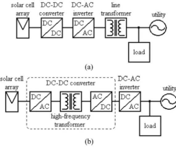
Fig. 1. Grid-connected photovoltaic generation system with an isolation trans-former. (a) Line frequency transtrans-former. (b) High-frequency transtrans-former.
green architecture. The use of thin-film solar cells has increased steadily and this trend is set to continue in the future.
In general, an earth parasitic capacitance will be generated between solar modules and their ground. This parasitic capac-itance is about 50–150 nF/kW for a glass-faced solar cell ar-ray [4], [13]. However, this capacitance is increased to 1 μF/kW if the thin-film solar cell array is used [4]. Serious leakage cur-rent occurs if a high-frequency pulsating voltage is applied be-tween the thin-film solar modules and the ground [4], [14], [15]. Corrosion damage in thin-film modules, caused by a so-called transparent conductive oxide (TCO) corrosion of cadmium tel-luride (Cd-Te) or amorphous silicon (A-Si), is observed if the voltage of the negative terminal of a solar module is lower than that of the ground. The damage to the electrical conductivity of the inside of the glass cover cannot be repaired and causes sub-stantial power loss [16]. Consequently, the life of thin-film solar modules is shortened [7], [17], [18]. However, TCO corrosion can be prevented by the negative grounding of solar modules.
Using an isolation transformer in the grid-connected inverter can solve the problem of the leakage current caused by the earth parasitic capacitance in solar modules. There are two types of grid-connected inverter with an isolation transformer. One is a line frequency transformer, and the other is a high-frequency transformer. Fig. 1(a) shows a grid-connected photovoltaic gen-eration system with a line frequency transformer. The solar modules can be grounded directly and there is no current path for leakage current because the line frequency transformer is isolated [4], [19]. This system supplies no dc current to the grid and has the advantage of a simple control circuit. However, the 0885-8993/$26.00 © 2011 IEEE
line frequency transformer’s disadvantages are large volume, high weight, and high cost.
Fig. 1(b) shows a grid-connected photovoltaic generation sys-tem with a high frequency transformer. The transformer is incor-porated in a dc–dc converter and is operated at high frequency to reduce volume and cost. However, the control circuit of this grid-connected photovoltaic generation system is complicated due to the use of a transformer-isolated dc–dc converter. Be-sides, the high-frequency transformer is not placed at the output of the grid-connected photovoltaic generation system, so it can-not prevent the dc current from injecting the grid.
The use of an isolation transformer in the grid-connected photovoltaic generation system should be avoided due to cost, size, and efficiency. In general, the bridge-type dc–ac inverter is used in the grid-connected photovoltaic generation system [15]. However, a conventional bridge-type dc–ac inverter, without an isolation transformer, results in the problem of leakage current because it cannot sustain the voltage of its negative terminal at a constant value. Recently, many dc–ac inverter topologies have been proposed to solve the problem of leakage current [7], [10], [14], [18], [20]–[23].
Lopez et al. proposed a diode-clamped multilevel dc–ac in-verter [20]; Chen et al. proposed a hybrid diode-clamped multi-level dc–ac inverter [10]. In a multimulti-level dc–ac inverter, two split capacitors are connected to the dc bus of a dc–ac inverter and the middle point is connected to the neutral line of the utility. The two voltage terminals on the dc bus of a dc–ac inverter are clamped. No pulsating voltage is applied between the thin-film solar modules and the ground. So, the leakage current is sup-pressed. Ma et al. proposed Conergy neutral point clamped to simultaneously improve the efficiency of a diode-clamped mul-tilevel inverter and overcome the leakage current problem [21]. Gonzalez et al. proposed the dc–ac inverter and Yu et al. pro-posed the H6 dc–ac inverter, in which one or two switches are combined with a full-bridge inverter to reduce the leakage cur-rent [14], [22]. Xiao et al. proposed several topologies to solve the problem of leakage current [23].
Although the aforementioned transformerless dc–ac inverter topologies can solve the leakage current problem, the negative grounding required in Cd-Te and A-Si thin-film solar cell array still cannot be solved. Boeke and van der Broeck proposed a three-phase four-wire dc–ac inverter with a split-capacitor arm where the middle point of the split-capacitor arm is connected to the neutral line of the three-phase four-wire distribution power system [7]. A buck-boost converter is used to build up the nega-tive bus voltage. Araujo et al. proposed a novel grid-connected nonisolated converter with a grounded generator [18]. A novel dc–dc converter is applied to generate two dc capacitor voltages of the half-bridge dc–ac inverter where a transformer (coupling inductor) is integrated in the dc–dc converter to achieve the neg-ative grounding of the solar cell array. The negneg-ative terminal of the solar cell array of the aforementioned two topologies can be directly connected to the ground, so the problems of leakage current and negative grounding are solved simultaneously.
This paper proposes a transformerless grid-connected power converter with negative grounding for a photovoltaic generation system. The proposed transformerless grid-connected power
converter simultaneously solves the problems of leakage cur-rent and negative grounding as the topologies shown in [7] and [18]. The negative grounding of the solar cell array in the proposed paper is achieved by a boost dc–dc converter and select switches. Therefore, the problem of TCO corrosion in Cd-Te or A-Si thin-film solar modules is also solved. Finally, a proto-type was developed and tested to verify the performance of the proposed transformerless photovoltaic generation system.
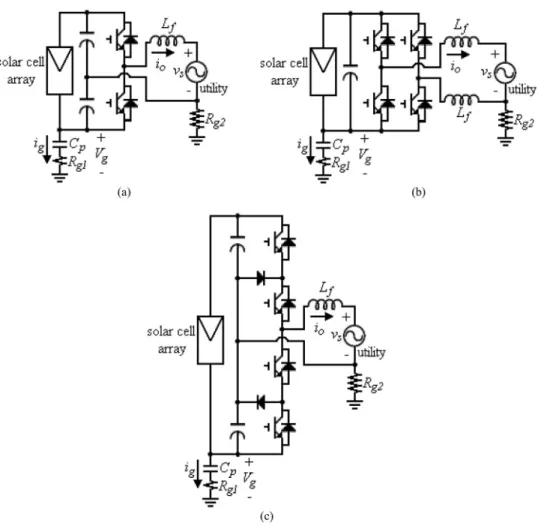
II. LEAKAGECURRENT OF ADC–AC INVERTER This section analyzes and discusses the problem of leakage current in a grid-connected photovoltaic generation system that uses a conventional half-bridge inverter, a conventional full-bridge inverter, and a diode-clamped multilevel half-full-bridge in-verter. Fig. 2 shows the relevant circuit configurations. In the following analysis, the capacity of the solar cell array shown in Fig. 2 is assumed to be 1 kW. An equivalent capacitor Cp
is serially connected to an equivalent resistor Rg 1 to represent
the parasitic elements of the solar cell array, and these are con-nected between the negative terminal of the solar cell array and the ground. The utility is connected to the ground by an equiva-lent resistor Rg 2. The capacitance of the parasitic capacitor Cp
is typically 1 μF in a 1-kW solar cell array. Since the utility voltage is 120 V, Rg 2 must be lower than 25 Ω to satisfy the
requirements [24]. Fig. 2(a) shows a conventional half-bridge inverter, which is controlled by pulsewidth modulation (PWM) and named as type 1. Fig. 2(b) shows a conventional full-bridge inverter. The conventional full-bridge inverter can be controlled by a bipolar PWM or a unipolar PWM, named as type 2 and type 3, respectively. Fig. 2(c) shows the diode-clamped multi-level half-bridge inverter named as type 4. A filter inductor Lf
connected to the output of the dc–ac inverter is used for filtering the switching harmonic of the dc–ac inverter.
Table I shows the main parameters of the simulation sys-tem. Fig. 3 shows the simulation results for the resistors Rg 1=
1 Ω and Rg 2 = 1 Ω. As can be seen, the grounding voltage vg
and the leakage current ig differ for different types of dc–ac
inverters. For the conventional half-bridge and diode-clamped multilevel half-bridge inverters (type 1 and type 4), the neutral line of the utility is directly connected to the middle point of the split dc capacitors. The voltage between the negative terminal of the solar cell array and the ground is stabilized by the lower dc capacitor of these types of dc–ac inverters. As seen in Fig. 3, the voltage of the negative terminal for these types of dc–ac inverters is−200 V. A voltage ripple with a frequency equaling that of the utility is incorporated in the voltage of the negative terminal because the ac current connected to the utility passes through the split dc capacitors. This voltage ripple is very small and depends on the capacitance of the split dc capacitors. Since the impedance of the earth parasitic capacitance is very large at the utility frequency, the leakage current of the utility frequency is very small. Fig. 3 shows a small high-frequency leakage cur-rent in the half-bridge inverter. This is due to the equivalent ground resistor Rg 2of the utility and switching operation of the
power electronic switches. However, the leakage current for the half-bridge inverter is less than 2.5 mA.
Fig. 2. Inverter topologies used in the grid-connected photovoltaic generation system. (a) Conventional half-bridge inverter. (b) Conventional full-bridge inverter. (c) Diode-clamped multilevel half-bridge inverter.
TABLE I
MAINPARAMETERS FORDIFFERENTINVERTERSUSED IN THESIMULATION
During the positive half-cycle of the utility voltage, the switching operation occurs at the upper side of the diode-clamped multilevel half-bridge inverter and results in a switch-ing ripple in the upper side capacitor. However, the voltage of the lower side capacitor is sustained and no leakage current is generated between the negative terminal and the ground. Simi-larly, this switching ripple will appear in the lower side capacitor during the negative half-cycle of the utility voltage and result in a small leakage current between the negative terminal and the ground. However, the leakage current for the diode-clamped multilevel half-bridge inverter is still less than 2 mA.
As seen in Fig. 2(b), the two lines from the utility are con-nected to the midpoints of two power electronic switch legs of a conventional full-bridge dc–ac inverter. To achieve symmetrical
circuit configuration and better suppress the leakage current, two filter inductors are connected between the outputs of the dc–ac inverter and the utility, respectively. As can be seen in Fig. 3, the voltage at the negative terminal of type 2 is a voltage ripple with a dc offset. The amplitude, frequency, and dc offset are 90 V, 60 Hz, and−100 V, respectively. The voltage at the neg-ative terminal of type 2 contains no pulsating voltage at the switching frequency due to the symmetric switching of the bipo-lar PWM. Since this voltage ripple is low frequency, the peak value of the leakage current is smaller than 50 mA. However, this leakage current is larger than that of the conventional half-bridge and the diode-clamped multilevel half-half-bridge inverters.
Fig. 3 also shows that the voltage at the negative terminal of type 3 contains a pulsating voltage with a frequency equaling the switching frequency due to the asymmetric switching of the unipolar PWM. The magnitude of this pulsating voltage is 90 V and results in a serious leakage current (about 1A) through the parasitic capacitance of the solar cell array.
Fig. 4 shows the simulation results for resistors Rg 1 = 10 Ω
and Rg 2= 10 Ω. As can be seen, the simulation results are similar
to those of Fig. 3. From the simulation results shown in Figs. 3 and 4, it can be seen that the leakage current in the conventional full-bridge inverter controlled by the unipolar PWM is too large to comply with the standard VDE 0126-1-1 [25].
Fig. 3. Simulation results for different types of inverter under 1 μF, Rg 1 =
1 Ω, and Rg 2= 1 Ω.
The major reason for grounding connection is safety. In prac-tical applications, the grounding resistance is usually very small. The earth parasitic capacitance, between the solar cell array and the ground, will cause leakage current and result in additional power loss. Table II shows the calculated power loss caused by the leakage current for the same earth parasitic capacitance (1 μF) and different resistors Rg 1 and Rg 2 (1 Ω, 5 Ω, and
10 Ω) in a 1-kW solar cell array [10], [26]. The power loss is the product of the square of the leakage current and the sum-mation of equivalent resistors Rg 1 and Rg 2. As can be seen
in Table II, the leakage currents are small in the conventional half-bridge inverter, the conventional full-bridge inverter with bipolar PWM, and the diode-clamped multilevel half-bridge in-verter. As seen in Table II, the power loss caused by the leakage current in types 1, 2, and 4 is very small. However, the power loss caused by the leakage current is significant in type 3, and it will evidently degrade the system efficiency. Besides, it can also be found that the calculated power loss of type 3 increases as the resistance is increased. Additionally, the leakage current will cause additional power loss at the filter inductor and power
elec-Fig. 4. Simulation results for different types of inverter under 1 μF, Rg 1=
10 Ω, and Rg 2= 10 Ω.
tronic switches. The power loss caused by the leakage current of type 3 will be higher than 1% in practice after considering the effects of both the parasitic and nonparasitic components.
III. CIRCUITCONFIGURATION
Fig. 5 shows the circuit configuration of the proposed photo-voltaic generation system. As can be seen, the grid-connected power converter is transformerless, and its negative terminal is connected directly to the ground. Both the problems of TCO corrosion and leakage current in Cd-Te or A-Si thin-film so-lar cell array can be avoided. The proposed transformerless grid-connected power converter is composed of a dc–dc power converter and a dc–ac inverter. The dc–dc power converter is a boost converter. The dc–dc power converter consists of three dc capacitors C1, C2, and C3, an inductor L1, two diodes D1 and D2, and four power electronic switches G1, G2, G3, and G5. The dc–dc power converter converts the dc voltage of the solar cell array to a stabilized dc voltage. The dc–ac inverter consists of two dc capacitors C2 and C3, an ac inductor Lf, and four
Fig. 17. Experimental results of the grid-connected power converter under the distorted utility voltage. (a) Utility voltage. (b) Output current of the dc–ac inverter.
Fig. 18. Experimental results for the power efficiency of the grid-connected power converter under different output power.
0 V and contains nearly no high frequency component. The leakage current ig, passing through the simulated capacitor and
resistor, is shown in Fig. 16(d). It is smaller than 10 mA. Be-cause of the small ripple for the negative terminal voltage of the proposed transformerless grid-connected power converter, the leakage current complies with the requirement stated in the VDE 0126-1-1 standard [25]. This effectively demonstrates that the proposed transformerless grid-connected power converter can not only solve the problem of TCO corrosion but also the problem of leakage current.
Fig. 17 shows the experimental results of the grid-connected power converter under the distorted utility voltage. The THD% of the distorted utility voltage shown in Fig. 17(a) is 7.5%. As seen in Fig. 17(b), the output current of the dc–ac inverter is still very close to sinusoidal. The THD% of output current of the dc–ac inverter is only 3.4%. This experiment verifies that the output current of the proposed grid-connected power converter can generate a sinusoidal output current even when the utility voltage is distorted.
Fig. 18 shows the experimental results for the power effi-ciency of the grid-connected power converter under different output powers. The solar cell array was replaced by a dc power supply to simplify the adjustment of output power in the exper-imental process. The output voltage of the dc power supply was set at 175 V. As can be seen, the power efficiency is 95.31% at full load and the maximum efficiency is 96.68%. The European efficiency is 96.17%.
VII. CONCLUSION
This paper proposes a novel transformerless grid-connected power converter. The negative terminal of the solar cell array can be directly connected to the ground in the proposed grid-connected power converter. The salient features of the proposed power converter are only two power electronic switches of the power converter are operated at high switching frequency si-multaneously (one is a dc–dc power converter and the other is a dc–ac inverter), and the negative terminal of the solar cell array is directly connected to the ground to solve the problems of TCO corrosion and leakage current for some types of thin-film solar cell array. The experimental results show that the proposed grid-connected power converter can trace the maximum power point of the solar cell array, convert solar power to a high quality ac power to inject into the utility, and reduce the leakage current of the solar cell array.
ACKNOWLEDGMENT
The authors would like to thank ABLEREX Corporation, Ltd., Irwindale, CA, for the financial and technical support in this paper.
REFERENCES
[1] T. Suntio, J. Leppaaho, J. Huusari, and L. Nousiainen, “Issues on solar-generator interfacing with current-fed MPP-tracking converters,” IEEE
Trans. Power Electron., vol. 25, no. 9, pp. 2409–2419, Sep. 2010.
[2] S. L. Brunton, C. W. Rowley, S. R. Kulkarni, and C. Clarkson, “Maximum power point tracking for photovoltaic optimization using ripple-based extremum seeking control,” IEEE Trans. Power Electron., vol. 25, no. 10, pp. 2531–2540, Oct. 2010.
[3] L. Maharjan, S. Inoue, H. Akagi, and J. Asakura, “State-of-charge (SOC)-balancing control of a battery energy storage system based on a cascade PWM converter,” IEEE Trans. Power Electron., vol. 24, no. 6, pp. 1628– 1636, Jun. 2009.
[4] J. M. A. Myrzik and M. Calais, “String and module integrated inverters for single-phase grid connected photovoltaic systems—a review,” in Proc.
IEEE Bologna Power Tech Conf., Jun. 23–26, 2003, vol. 2, pp. 1–8.
[5] J. Leppaaho and T. Suntio, “Dynamic characteristics of current-fed super-buck converter,” IEEE Trans. Power Electron., vol. 26, no. 1, pp. 200–209, Jan. 2011.
[6] A. Koran, K. Sano, R. Y. Kim, and J. S. Lai, “Design of a photovoltaic simulator with a novel reference signal generator and two-stage LC output filter,” IEEE Trans. Power Electron., vol. 25, no. 5, pp. 1331–1338, May 2010.
[7] U. Boeke and H. van der Broeck, “Transformer-less converter concept for a grid-connection of thin-film photovoltaic modules,” in Proc. IEEE Ind.
Appl. Soc. Annu. Meet., Oct. 5–9, 2008, pp. 1–8.
[8] Y. Sozer and D. A. Torrey, “Modeling and control of utility interactive inverters,” IEEE Trans. Power Electron., vol. 24, no. 11, pp. 2475–2483, Nov. 2009.
[9] Z. Liang, R. Guo, J. Li, and A. Q. Huang, “A high-efficiency PV module-integrated DC/DC converter for PV energy harvest in FREEDM systems,”
IEEE Trans. Power Electron., vol. 26, no. 3, pp. 897–909, Mar. 2011.
[10] A. Chen, W. Wang, C. Du, and C. Zhang, “Single-phase hybrid clamped three-level inverter based photovoltaic generation system,” in Proc. IEEE
Int. Symp. Power Electron. Distrib. Generation Syst., Jun. 16–18, 2010,
pp. 635–638.
[11] X. Li and A. K. S. Bhat, “Analysis and design of high-frequency iso-lated dual-bridge series resonant DC/DC converter,” IEEE Trans. Power
Electron., vol. 25, no. 4, pp. 850–862, Apr. 2010.
[12] J. I. Itoh and F. Hayashi, “Ripple current reduction of a fuel cell for a single-phase isolated converter using a DC active filter with a center tap,”
IEEE Trans. Power Electron., vol. 25, no. 3, pp. 550–556, Mar. 2010.
[13] T. Kerekes, M. Liserre, R. Teodorescu, C. Klumpner, and M. Sumner, “Evaluation of three-phase transformerless photovoltaic inverter topologies,” IEEE Trans. Power Electron., vol. 24, no. 9, pp. 2202–2211, Sep. 2009.
[14] R. Gonzalez, J. Lopez, P. Sanchis, and L. Marroyo, “Transformerless inverter for single-phase photovoltaic systems,” IEEE Trans. Power
Elec-tron., vol. 22, no. 2, pp. 693–697, Mar. 2007.
[15] M. Calais and V. G. Agelidis, “Multilevel converters for single-phase grid connected photovoltaic systems-an overview,” in Proc. IEEE Int. Symp.
Ind. Electron., Jul. 7–10, 1998, vol. 1, pp. 224–229.
[16] H. Schmidt, “Do thin-film modules need special inverters?” presented at the Fifth User Forum Thin-Film Photovoltaics, W¨urzburg, Germany, Jan. 26–28, 2009.
[17] C. R. Osterwald, T. J. McMahon, J. A. del Cueto, J. Adelstein, and J. Pruett, “Accelerated stress testing of thin-film modules with SnO2:F transparent conductors,” in Proc. National Center Photovoltaics Solar Program Rev.
Meet., Mar. 24–26, 2003, pp. 1–4.
[18] S. V. Araujo, P. Zacharias, and B. Sahan, “Novel grid-connected non-isolated converters for photovoltaic systems with grounded generator,” in
Proc. IEEE Power Electron. Spec. Conf., Jun. 15–19, 2008, pp. 58–65.
[19] L. Quan and P. Wolfs, “A review of the single phase photovoltaic module integrated converter topologies with three different DC link configura-tions,” IEEE Trans. Power Electron., vol. 23, no. 3, pp. 1320–1333, May 2008.
[20] O. Lopez, R. Teodorescu, and J. Doval-Gandoy, “Multilevel transformer-less topologies for single-phase grid-connected converters,” in Proc. IEEE
Conf. Ind. Electron., Nov. 6–10, 2006, pp. 5191–5196.
[21] L. Ma, T. Kerekes, R. Teodorescu, X. Jin, D. Floricau, and M. Liserre, “The high efficiency transformer-less PV inverter topologies derived from NPC topology,” in Proc. Eur. Conf. Power Electron. Appl., Sep. 8–10, 2009, pp. 1–10.
[22] W. Yu, J. S. Lai, H. Qian, C. Hutchens, J. Zhang, G. Lisi, A. Djabbari, G. Smith, and T. Hegarty, “High-efficiency inverter with H6-type config-uration for photovoltaic non-isolated ac module applications,” in Proc.
IEEE Appl. Power Electron. Conf. Expo., Mar. 18, 2010, pp. 1056–1061.
[23] H. Xiao and S. Xie, “Leakage current analytical model and application in single-phase transformerless photovoltaic grid-connected inverter,” IEEE
Trans. Electromagn. Compat., vol. 52, no. 4, pp. 902–913, Nov. 2010.
[24] IEEE Guide for Safety in AC Substation Grounding, IEEE Standard 80-2000, Jan. 2000.
[25] Automatic Disconnection Device Between a Generator and the Public
Low-Voltage Grid, Standard DIN VDE 0126-1-1, Feb. 2006.
[26] O. Lopez, F. D. Freijedo, A. G. Yepes, P. Fernandez-Comesaa, J. Malvar, R. Teodorescu, and J. Doval-Gandoy, “Eliminating ground current in a transformerless photovoltaic application,” IEEE Trans. Energy Convers., vol. 25, no. 1, pp. 140–147, Mar. 2010.
[27] H. L. Jou, K. D. Wu, J. C. Wu, and J. M. Shen, “Simplified maximum power point tracking method for the grid-connected wind power genera-tion system,” Electr. Power Compon. Syst., vol. 36, no. 11, pp. 1208–1217, Nov. 1, 2008.
[28] T. J. Liang and J. L. Shyu, “Improved DSP-controlled online UPS system with high real output power,” IEE Proc. Electr. Power Appl., vol. 151, no. 1, pp. 121–127, Jan. 9, 2004.
Jia-Min Shen (S’08) was born in Tainan, Taiwan,
in 1982. He received the M.S.E.E. degree from the National Kaohsiung University of Technology, Kaoh-siung, Taiwan, in 2005. He is currently working to-ward the Ph.D. degree in electrical engineering from the National Kaohsiung University of Applied Sci-ences, Kaohsiung.
His research interests include power electronics applications and DSP control.
Hurng-Liahng Jou (M’99) was born in Taiwan in
1959. He received the B.S.E.E. degree from Chung Yuan University, Jonglih, Taiwan, in 1982, and the M.S.E.E and Ph.D.E.E. degrees from National Cheng Kung University, Tainan, Taiwan, in 1984 and 1991, respectively.
He is currently a Professor in the Department of Electrical Engineering, National Kaohsiung Univer-sity of Applied Sciences, Kaohsiung, Taiwan. His research interests include power electronics applica-tions and power quality improvement technique.
Jinn-Chang Wu (M’07) was born in Tainan, Taiwan,
in 1968. He received the M.S.E.E. and Ph.D.E.E. de-grees from National Cheng Kung University, Tainan, Taiwan, in 1992 and 2000, respectively.
He is currently an Associate Professor in the De-partment of Microelectronics Engineering, National Kaohsiung Marine University, Kaohsiung. His re-search interests include power quality and power electronics applications.