[
Student Paper
1
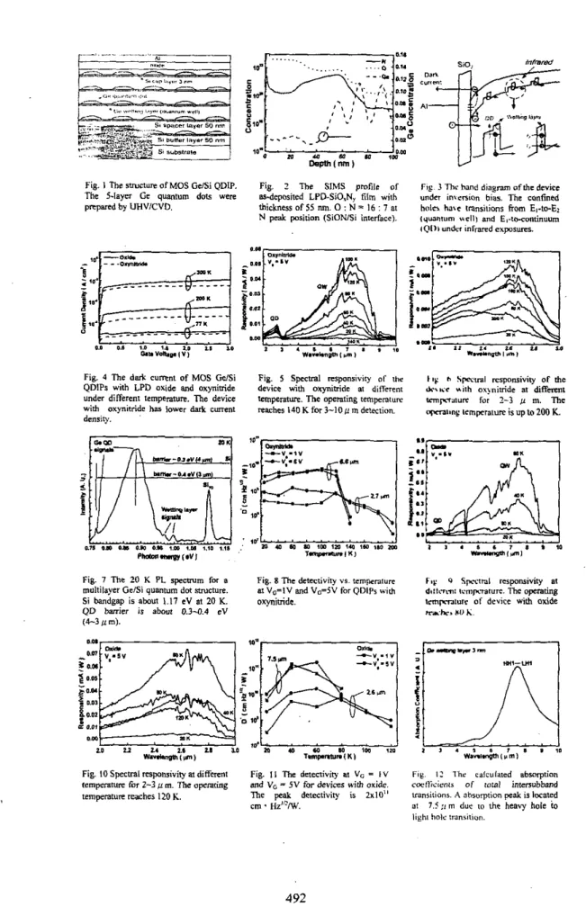
MOS Ge/Si Quantum Dot Infrared Photndetectors,with Quantum Dot and
Wetting Layer Responses
E X .
Hsu',S.
T.
Changb,
P.-S. Kuu',P. S .
Chen', C.
W.
Liu'", J.-H.
Lu', and C.
H. Kuan'
'Department o f Electrical Engineering and Graduate Institute o f Electronics Engineering,National Taiwan University, Taipei, Taiwan,
R.
0. C.
Department of Electronic Engineering, Chung Yuan Christian University, Chung-Li, Taiwan, R. 0. C .
ERSOIITRI, Hsinchu, Taiwan, R. 0. C. E-mail: cheeil7!cc.ee.ntu.rdu.tw
Due to low dark current, high operation temperature and normal incident detection, the quantum dot infrared photodetector (QDIP) using the intervalence band transitions
is
very attractive in the military, medical, astronomical and other applications. The simple metal-insulator-semiconductor (MIS) structure with tunneling insulator can make the GeISi QDIP compatible with Si ULSl process, and make it possible to have convenient and accurate body temperature measurement using a S i chip. A 5-period self-assembled Ge/Si quantum dots with3
nm wetting layers (quantum well) grown by UHVICVD (Fig. I) is fabricated into MIS tunneling diodes [I] with low temperature (50°C) liquid phase deposition (LPD) oxide and oxynitride [2]. The existence
o f N in
oxynitride is confirmed by SlMS (Fig. 2).The dark current o f MIS tunneling diode is dominated by thermal generation o f electron-hole pairs through the defects in the depletion region and at the Si/Si02 interface (Fig. 3). The LPD oxynitride has a low interface density, and thus has a low dark current a5 compared to LPD oxide (Fig. 4). T h e thermally-generated electrons tunnel through the insulator layer and the thermally-generated holes in deep depletion region as well as the holes tunneling
from
gate electrode are swept toward the substrate. Due to the large valence band offset formed in G d S i heterojunctions, the hole densities are high in the Ge quantum layers. The Ge quantum dots are placed in the depletion region at inversion bias to have electrical field to drift the photo-excited holes. Under infrared exposures, the confined holes have bound-to-bound (quantum well) andThe spectral responsivity o f the NMOS Ge/Si QDlP with oxynitride has two absorption regions (2-3p m and 3-lOpm, Fig.
5).
For 3-IO@ m detection, the peak wavelengthis
located at 6 . 8 , ~ m and the maximum operating temperature i s about 140 K. For 2-3 p m detection, the peak wavelength is located at 2.7 m and the operating temperature i s up to 200 K (Fig.6).
Sincethe operating temperature
i s higher for2-3
p m detection, this short wavelength response mainly comes from the quantum dot structure due to the better quantum confinement, while the 3 - l o p m response is dominated by the wetting layer structure. The photoluminescence (PL) spectrum also confirms that the short wavelength response comes form the quantum dot structure with the larger barrierfor
bound-to-continuum transition (0.3-0.4 eV, Fig. 7) [3]. The peak detectivity is IO'' and IOn cm.
Hz"/W for 6.8 p m and 2 . 7 , ~ m, respectively (Fig. 8). The MOS GeISi QDIP with LPD oxide has'a stronger responsivity as compared to the device with LPD oxynitride (Fig. 9). However, the operating temperature i s only 80 K for 3-10pm detection and is 120 K for2-3
,Um detection (Fig.
IO). The lower operation temperature is due to the larger dark current of oxide devices (Fig. 4). The7.S
p m detectivity at 60 K reaches 2x10'' cm.
Hz'"/W (Fig. I I).The valance band bound state energy o f wetting layer is calculated by
k
9 p method. Bycalculating the total intersubband transitions, a absorption peak i s located at 7 . 5 ~ m (Fig.
12).
The theoretical results show good agreement with the experimental spectrum and confirmed that the long wavelength response mainly comes from the wetting layer structure (quantum well).The MOS GeiSi QDlPs for 2-10 p m are successfully demonstrated. Using oxynitride as gate dielectric, the operating temperature reaches 140 K for 3 - I O u m and i s up to 200 K for
2-3
p m detection. The quantum dot structure is responsible for 2-3 fi m response with high operation temperature. This novel MOS GeISi QDlP can increase the functionality of S i chip and is fully compatible with ULSl technology.[ I ] C. W. Liu et al., IEDM Tech. Dig., pp.749-752, 1999. [2] B.-C. Hsuetal., IEDM Tech. Dig., pp.91-94, 2002.
13) Vinh Le Thanh el al., J. Vac. Sci. Technol. B 20(3), pp.1259-1265,2002.
_ _
Fig. 4 The dark current of MOS GelSi Fig. 5 Spesval xsponriviry of Ulr I t y h S m ' v a l rerponriviry of the
QDlPr with LPD axids and oxynitridc device with oxyniuidc 81 different *%IEC uiih aqniuide a! diffmnt
under different temparaturr. The device temperam. The operating temperauw m p n r ! v r r fur 2-3 U m. The
with mynitride has lower M c m t macher 140 K for 3-10 P m dewdon.
density. ~ c m p e m t u ~ is up to 200 K.
fig. 1 The 20 K PL s~permm for B Fig. 8 The deieciiviry VI. tmnmmturr f P Spuiml mrponriviry at
multilayer GelSi quantum dot m c f y ~ . adfnmi ~cmpmrurc. The operating
Si bandgap is abut 1.17 CV st 20 K. ionpmiurr of device with oxide
QD barrier is about 0.3.04 sV ?radw XI) L
(4-3 P m).
at V,=IV and VI;=5V for QDlPr with oxynimda.
Fig. IOSpecVdl~ponsi~iryatdiffersnt Fig. I 1 The dnecriviry I V, = I v Fig I: lhr. calculated abmorptian
temperature for 2-3 p m. The aperaring and V, = 5V for devices with oxide. cu.lli~.i~.ob of ioul intcnubband
temperature reacher 120 K, The pe& deieftiviry i s 2x10" mniitioni. h ahsorption pb is lceted
7.C :I m due to I h c heavy hole io
cm
.
W'iW. ailight holc trmsition.