行政院國家科學委員會專題研究計畫 成果報告
兼具偵測多波段紅外線及可見光的偵測器陣列模組之研發
(3/3)
計畫類別: 個別型計畫 計畫編號: NSC93-2215-E-002-002- 執行期間: 93 年 08 月 01 日至 94 年 07 月 31 日 執行單位: 國立臺灣大學電子工程學研究所 計畫主持人: 管傑雄 計畫參與人員: 盧仁祥 報告類型: 完整報告 報告附件: 出席國際會議研究心得報告及發表論文 處理方式: 本計畫可公開查詢中 華 民 國 94 年 10 月 25 日
行政院國家科學委員會補助專題研究計畫
■ 成 果 報 告
□期中進度報告
兼具偵測多波段紅外線及可見光的偵測器陣列模組之研發(3/3)
計畫類別:
█個別型計畫 □ 整合型計畫
計畫編號:NSC 93-2215-E -002-002-
執行期間:2004 年 08 月 01 日至 2005 年 07 月 31 日
計畫主持人:
管傑雄
共同主持人:
計畫參與人員: 盧仁祥,蕭學鈞,黃逵謙,謝寬洲,吳坤政
成果報告類型(依經費核定清單規定繳交):
□精簡報告 ■完整報告
本成果報告包括以下應繳交之附件:
□赴國外出差或研習心得報告一份
□赴大陸地區出差或研習心得報告一份
█出席國際學術會議心得報告及發表之論文各一份
□國際合作研究計畫國外研究報告書一份
處理方式:除產學合作研究計畫、提升產業技術及人才培育研究計畫、
列管計畫及下列情形者外,得立即公開查詢
█
涉及專利或其他智慧財產權,□一年
█二年後可公開查詢
執行單位: 台大電子所
中 華 民 國 2005 年 09 月 28 日
目錄
摘要 III
Abstract IV
一、計畫內容
1
1. Quantum Well Infrared Photodetector with V-groove
Structure for Normal Incident Light Coupling
1
A. 前言 1
B. 研究方法 2
1. Coupling Efficiency Estimation
2
2. Anisotropic Wet Etching
6
C. 結果與討論 7
D. 結論與計畫自評 11
E. 參考文獻 11
2. Superlattice Infrared Photodetector and 1-D Detector Array
13
A. 前言 13
B. 研究方法 13
1.
Fabrication Process of the Single Photodetector13
2.
Fabrication Process of the 1-D Detector Array16
C. 結果與討論 20
1. SLIP with Doping Density 1Ⅹ1017 in the Superlattice
20
2. SLIP with Doping Density 5Ⅹ1016 in the Superlattice
27
4. 1-D Detector Array
34
5. Comparison of Single Device and 1-D Detector Array
35
D. 結論與計畫自評 44
E. 參考文獻 44
3. Superlattice Infrared Photodetector with Grating Structure for
Normal Incident Light Coupling
46
A. 前言 46
B. 研究方法 47
C. 結果與討論 50
1. Sample with 45-degree facet coupling
50
2. Samples with grating structure
51
3. Discussion
56
D. 結論與計畫自評 63
E. 參考文獻 63
二、參考文獻
63
摘要
紅外線在日常生活方面的應用越來越廣泛,包含了國防,天文,環保以及醫 療等等。而現今世界各國都有許多公司與研究機構開始發展焦平面陣列的紅外線 偵測器,以期能達到較大面積與較準確的應用。但量子井或超晶格紅外線偵測器 因為受到電子躍遷的選擇律的限制,需要一個與長晶方向相同的電場來達成激發 電子的目的,所以並不能吸收正向入射的光線。一般在做單顆元件的特性量測 時,我們可以在樣品的側邊磨四十五度斜角,讓光線從斜面入射,使得紅外線有 垂直方向的電場。但在大型的焦平面陣列,並不能利用此一概念,而需要其他的 方式讓紅外線可以經由正向的入射來達成偵測的效果。在此計畫中,我們提出了 數種方式,分別是V 型谷結構來達成耦合垂直入射光的目標,並進而開發此結 構的一維線性陣列,以及利用金屬層上的週期性排列的孔洞,達成正向入射的目 的。 運用非等向性化學蝕刻在量子井偵測器上製作 V 型谷結構,可以耦合垂直 入射之光線。我們利用幾何光學來估計具 V 型谷結構之量子井偵測器耦合垂直 入射光的效率﹔並提出一套製作程序,用來製作具 V 型谷結構之量子井偵測 器。由光電流響應的量測顯示,V 型谷結構耦合垂直入射光的能力可大致等效於 45∘角斜面角 TM 模式的入射。 若要將其應用在紅外線熱影像時,此偵測器除了要有較高的背景限制效率溫 度之外,還必須以一維或二維的大型焦平面陣列來取代單一的偵測器元件。我們 也介紹了一維偵測器陣列的製程步驟,將元件做成陣列的型式。實驗結果顯示雖 然此一維偵測器陣列的響應峰值較單一偵測器元件要來的小,但是由於其暗電流 也比單一偵測器元件要小的多,所以其偵測度反而比單一元件要來的好。由結果 顯示,我們可以藉由增加環狀金屬的接觸面積,以及增加 V 型凹槽的傾斜角度, 來提高偵測器陣列的響應度。在製做一維偵測器陣列時,此製程步驟是一項不錯 的選擇。 在元件製程上,我們也可以在樣品表面設計一具有週期性結構的金屬孔洞, 以類似光子晶體的概念,形成另類的光柵,而使得此偵測器可以達到頂面正向入 射的目的,以避免底面入射必須磨薄的製程。 我們製作了三種不同週期的光柵結構,而光線由正面入射。我們可以利用各 種不同週期的光柵結構來調變響應的波形。這是因為響應的波形會受到表面電漿 共振的影響。而表面電漿共振的頻率可以用光柵的週期來控制。在本篇論文中, 我們成功地利用光柵結構製作出可以正向入射的紅外線偵測器,而且響應的波形 可以利用表面電將共振來調變。關鍵詞:量子井紅外線偵測器,超晶格紅外線偵測器,線性陣列,正向入射光耦 合,金屬條狀光柵
Abstract
Infrared detection has been used widely as the applications in military services, astronomy, environmental monitoring and medicine. In recent years, many companies and research institutes focused on the development of the infrared detector’s focal plane array to achieve the large area and more accurate detection applications. For quantum well or superlattice infrared photodetector, because of the selection rule, the photodetector does not absorb radiation incident normal to the surface since the light polarization must have an electric field component parallel to the growth direction. In general, the single photodetector device has to be illuminated through a 45∘polished facet. However, this illumination scheme limits the configuration of the detectors to linear array or large focal plane array. For imaging, it is necessary to be able to couple light uniformly to two-dimensional arrays of these detectors. In this paper, we will present several methods to achieve the goal of coupling the normal incident light, such as the photodetectors with V-groove structure for normal incident light coupling. Moreover, we fabricate the one-dimension linear array based on this structure. Besides, the periodic metal hole array is designed on the sample surface. This structure can act as the grating and make the detector achieve the goal of normal incidence.
V-groove structure can be fabricated on the QWIP by using anisotropic etching to couple the normally incident light. In this paper, the efficiency for the QWIPs with V-groove structure to couple the normally incident light is estimated by applying the ray optics. A feasible processing procedure for fabricating the V-groove structure is proposed. The responsivity measurement shows that the V-groove structure can couple the normal incident light with the same efficiency as the TM mode light incident into the 45∘edge facet of the photodetector.
For thermal imaging application, the detectors must have high background limited performance temperature TBLIP and 1-D or 2-D (Focal Plane) detector arrays have
been used instead of the single detector. The process of the linear array fabrication is also introduced. The experimental results show that the response of the detector array is smaller than single device, but the dark current of detector array is much smaller than single device. It leads to the larger detectivity of detector array. By increasing the contact area of metal ring and tilted angle of V-grooves for larger responsivity, it will be a new method to fabricate 1-D detector array.
For device fabrication, we can design a metal hole array with periodicity on the sample surface. Analogous to the concept of photonic crystal, the metal hole array can act as the grating and make the detector achieve the goal of normal incidence. The traditional fabrication of detector with normal incidence is to thin down the substrate.
Using this new structure, we can omit the thin-down process.
We fabricate three devices with different period of gratings for topside-illumination. Base on this structure, the photoresponse of each spectral shape is tunable by the period of gratings. The response shape is affected by surface plasmon. The plasmon peak can be selected by period of gratings. In summary, the experimental results confirm the applicability of SLIPs with grating structure for coupling the normal incident light and tunable response shape by surface plasmon.
Keywords:quantum well infrared photodetector, superlattice infrared photodetector, linear array, normal incident light coupling, metal strip grating
一、計畫內容
1. Quantum Well Infrared Photodetector with V-groove
Structure for Normal Incident Light Coupling
A. 前言
Quantum well infrared photodetectors (QWIPs) based on intersubband transition have been undergoing rapid development during the past several years. Infrared detectors made of GaAs/AlxGa1-xAs quantum well may be a potential alternative to
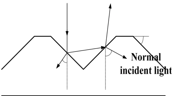
those based on HgCdTe material system because of the relative maturity of GaAs-related materials and their processing technology [1,2]. For most detector applications, normally incident radiation absorption is required for convenience. However, due to the isotropic effective mass of the active Γ electrons, the QWIP detector can only absorb light with the electric field perpendicular to the multiple quantum well layers [3,4,5]. In order to couple the normal incident radiation, much work has been done, such as two-dimensional grating, and random scattering couplers. Recently, a coupling scheme based on total internal reflection (TIR) instead of diffraction was proposed by C.J. Chen et al [6,7,8]. Referring to Fig. 1, this coupling scheme utilizes an array of QWIP wires with slant sidewalls to reflect the normally incident light. These QWIP wires are created by etching V-grooves through the detector active region to the bottom contact. In the ideal case showed in Fig. 1, the reflected light will propagate parallel to the MQW layers, and hence half of the photons can be absorbed for unpolarized light. Besides, the light can also be illuminated from the topside of the sample. On this condition, the light is coupled into the QWIP by refraction as shown in Fig. 2 instead of TIR.
Substrate
QW layers
Normal incident light
° 45
°
45
Fig. 2 Optical path for top-illuminated light.
Our work is to develop a method to estimate the coupling efficiency of V-groove structure and try to find the associated affecting factors. The processing steps to fabricate a QWIP with V-grooves are also proposed in this work for practical test. The responsivities of the QWIP with V-grooves are measured and compared with experimental results based on traditional edge coupling scheme. The IR absorpton spectrum and spectral response are also measured for comparison.
B. 研究方法
1. Coupling Efficiency Estimation
In this section, the responsivity of a QWIP with V-grooves is estimated and used as an index to evaluate the V-groove coupling scheme. The responsivity R of a detector, is defined as the ratio of the photocurrent Ip over the optical power Pi transmitted into
the detector, i.e.
g h e P I R d i p ν η = ≡ (1) where h is the photon energy, g is the photoconductive gain, and ν ηd is the quantum efficiency of the detector [9]. Among them, ηd is defined as average number of optical transitions per photon incident into the sample, and is given by
)] sin exp( 1 )[ 1 ( 2 1 2 * 0 2 θ ε η sN c m n W N f e R M A A w d Q c d = − − − Γ h , (2) where A is the area of the detector, Ac is the effective coupling area, M is the material removal factor, R is the reflection coefficient of the detector surface, s is the times that a photon passes the detector, N is the number of periods in a MQW structure, fQ is the oscillator strength, Nd is the doping density in the well, θ is the angle of incidence, W is the width of the well, nw and m* are the refractive index and the effective mass of
the well respectively, and Γ is the absorption linewidth [1]. The term (1/2) is used to count in the fact that only the component with the TM polarization can be absorbed for the unpolarized light. During fabricating a QWIP with V-grooves, some part of the MQW is removed by wet etching. The removal of material will affect the responsivity of the detector. Therefore, a parameter M is used to count in this effect.
In order to evaluate the coupling efficiency of V-groove coupling scheme, the edge coupling scheme that couples the incident light through a 45∘facet on the edge of the substrate is introduced first. The infrared light is back-illuminated onto the detector through the facet as illustrated in Fig. 3. Although the edge coupling is not useful for practical applications, it is still a standard to evaluate a QWIP’s intrinsic performance by virtue of the simple processing steps and the readily known light intensity inside the sample. It can also be a standard to evaluate another coupling scheme by comparing its responsivity with that of the edge coupling [1]. For convenience, a quantity named responsivity ratio (abbreviated as R ratio) is defined as
scheme coupling edge of η scheme coupling a of η ratio R d d = . (3)
The R ratio is the figure of merit of a particular coupling scheme and is independent on the quantum well parameters [1].
o 45 =
θ
Top contact Bottom contact Substrate QWIP o 45 = θ θ cos A Ac= A
Fig. 3 The light incident geometry under edge coupling. The light passes the QWIP two times.
o
45
With the definition of R ratio, the coupling efficiency of V-groove structure can be easily evaluated. All we need to do is plotting the optical path and substituting all related parameters into Eqs. (2) and (3) to calculate the R ratio. Since the light can be illuminated from backside or topside of the sample, we will discuss both conditions respectively.
coupled by the total internal reflection on the slant sidewall as shown in Fig. 4. The slope of the sidewall generated by wet etching is about 54∘instead of 45∘[10]. The light passes the detector by two times just the same as the edge coupling scheme. It is noted that the effective area Ac to couple the normal incident light is restricted by the area of sidewalls and varies with the geometry of the detector. The angle of incidence for TIR coupling scheme is 72∘ which is larger than 45∘for the edge coupling scheme. ° 18 ° 36 ° 54 o 72 = θ A effective coupling area Ac
Fig. 4 The optical path for the TIR coupling scheme in the V-groove structure. One may wish to reduce the width of QWIP wires in order to increase the number wires and hence the effective coupling area in a single detector pixel. When the sidewall separation is sufficiently narrowed, the optical path of the incident light will be different as shown in Fig. 5. This should be considered when designing the detector. ° 36 ° 54 ° 36 ° 18
Fig.5 The optical path of TIR coupling scheme when the width of the QWIP wires re sufficiently narrowed.
The top-illuminated situation is considered now. Referring to Fig. 6, 90% of the incident photon (TM mode) will pass through the air-GaAs interface and turns into a new direction by the refraction effect. The remaining 10% of photons are reflected and have 75% opportunity to enter the QWIP through another interface. We can calculate the R ratio easily as for the backside-illumination case. The R ratio for this condition is expected to be smaller than that in the backside-illumination case
° 54 ° 60 ° 39
Fig. 6 The optical path when the light is incident from the topside of the QWIP with -grooves.
d, the R ratio on this condition is less than that on the back-illuminated condition.
Number of V-grooves
ratio versus the number of V-grooves in a QWIP for V
To evaluate the efficiency and feasibility of the V-groove coupling scheme, we calculate the R ratio for a series of QWIPs with different number of V-grooves. The parameters of the MQW structure are assumed as Nd=1.2x1018cm-3, well width W=50 angstroms, oscillator strength fQ=1, number of wells N=30, and absorption linewidth Γ=20 meV. For a given QWIP, we calculated R ratio vs. the number of V-grooves within the QWIP. The result is shown in Fig. 7. For sufficiently large number of V-grooves, the R ratio is greater than one. The R ratio on top-illuminated condition is given in Fig. 8. As expecte
1
Fig. 7 The estimated value of R
R ratio 0.8 0.6 0.4 10 20 30 0.2 40
the back-illuminated condition.
Number of -grooves
R ratio versus the number of V-grooves in a QWIP for e top-illuminated condition.
2.
0.5
V Fig. 8 The estimated value of
th
Anisotropic Wet Etching
For anisotropic wet etching process, the slowest etching planes dictate the final shape of the etched profile. The [111] Ga planes therefore dominate the profile since the etching rate on [111] Ga is the slowest for most reaction-limited etchants. The etched profile generated by anisotropic etching is shown in Fig. 9. Typical reaction-rate-limited etchants yield outward sloping edges along [011] direction and inward sloping edges, i.e. trenching effect, along [011] dir . As the microscopic photographs shown in Fig. 10, the Q wires parallel
ection
WIP [011]direction
yield a perfect V-groove, while the wires parallel [011] direction almost disap due to the severe trenching effect. Thus, the wires on our mask should parallel
peared
] 1 01 [
direction to ensure the correct profile when fabricating the QWIP. On the other hand, the selection of the etchants is also important because the etching rate and angle of sidewall vary with etchants. After many tests on various etchants, the NH4OH-H2O2-H2O (3:1:50) etchant is selected to fabricate the QWIPs with V-grooves
because it has proper etching rate and yields a proper slope of sidewall, about 50∘.
R ratio 0.4 0.3 0.2 10 20 30 0.1 40
X Y Z ] 100 [ ] 001 [ ] 010 [ ) 100 ( GaAs ) 111 ( (111) ) 1 1 1 ( ) 1 1 1 ( o 74 . 54 = θ ] 011 [ ] 1 01 [
Fig. 9 The GaAs (100) wafer cleaved along (011) and (011) planes normal to the (100) surface. The etchants that etch the [111] Ga type planes as the slowest rates would yield anisotropic etch profile as shown.
ig. 10 The profile produced by the anisotropic etching process. The wires in the F
left photograph are parellel to the [011] direction and those in the right photograph are parallel to [011] direction.
C. 結果與討論
ent consists of 30 periods of GaAs quantum wells an
The MQW used in our experim
d Al0.25Ga0.75As barriers. The well width and the barrier width are 50 angstroms and 800 angstroms respectively. The doping density Nd is 1.2x10 18 cm−3 in the wells and 1.5x1018 cm−3 in the contact layers. Its detection peak λ
μm. Using thi ucture, a QWIP with V-grooves is fabricated to verify the expectation aforementioned. The 3-dimensional perspective of the device is shown in Fig. 11. This perspective is just for illustration, so the number of wires and distance between wires is different to the real device. The dimensions of real device are given in Fig. 12. Besides, the scanning electron microscopy (SEM) photographs are shown in Fig. 13 and Fig.14. The estimated R ratios of this QWIP for back-illuminated and top-illuminated case are 0.68 and 0.40 respectively.
s QW str
Fig. 11 3-dimensional perspective of the QWIP with V-grooves.
Fig.12 groove structure.
m μ 200 m μ 400 Top contact MQW layers m μ 150 22 periods
Dimension of the QWIP with
V-Fig. 13 SEM photograph of the QWIP with V-groove structure.
m μ 2 m μ 5 . 2 m μ 2 m μ 4 . 3 m period=9μ m μ 200
Fig. 14 SEM photograph the V-groove structure in our QWIP. The distance between ach QWIP wires is 9 μm
heme, the responsivity of QWIP with dge coupling scheme was firstly measured at various temperature and bias conditions.
Th he
greater than 60% of that measured with
from
ion are given in Fig. 18. The R ratio for the ba
e
To evaluate the V-groove coupling sc 45o
e
e structure of this QWIP is only a plane mesa without any V-grooves. T measured responsivity was shown in Fig. 15. Then, the QWIPs with V-grooves were measured for comparison. The QWIPs were illuminated by blackbody radiation from either backside and topside of the sample.
The responsivity with infrared radiation incident from backside of the sample was shown in Fig. 16. The responsivity is
oedge coupling scheme through the whole bias range. The results agree with our
estimation in section 2. Fig. 17 shows the responsivity with infrared radiation incident the topside of the sample. It is also greater than 60% of that measured with 45 o
edge coupling scheme through the whole bias range. The applicability of this coupling scheme is sure enough.
The responsivity ratios (R ratio) vs. bias voltage for both back-illuminated and top-illuminated condit
45
ckside-illumination is always larger than that of the topside one. The real value of the R ratio is a little bit larger than our estimation. It may be attributed to the absorption due to the multiple reflection, which is not taken into account in our estimation. In particular, for the bias dependence, it is noted that the R ratios at low bios region increase rapidly. This may be resulted from the variation of refractive index at the low bias region since the crystal structure of GaAs is polar and the refractive index change with bias. The further study is necessary to understand the reason.
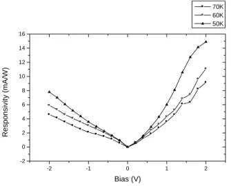
-2 -1 0 1 2 0 10 20 30 70K 60K 50K R e sp on siv ity (mA/W ) Bias (v)
Fig. 15 Responsivity of the QWIP with edge coupling scheme.
-2 -1 0 1 2 -2 0 2 4 6 8 10 12 14 70K 60K 50K 16 Respo n sivi ty (mA/ W ) Bias (V)
Fig. 16 Responsivity of the QWIP with V-groove on back-illuminated condition.
-2 -1 0 1 2 -2 0 2 4 6 8 10 12 14 70K 60K 50K 16 Respons iv it y (m A/ W ) Bias (V)
-2 -1 0 1 2 0.6 0.8 1.0 1.2 1.4 back-illuminated top-illuminated R r a tio Bias (V)
Fig. 18 Responsivity ratio (R ratio) of the QWIP with V-grooves at 50K. The R ratios on both top-illuminated and back-illuminated condition are calculated respectively.
D. 結論與計畫自評
The theoretical estimation model of the V-groove structure to couple the normally incident light with the quantum well infrared photodetector is proposed in this paper. A wet-etching process is given to fabricate the V-groove structure. The estimated R ratio is about 80% of the real value. The underestimation is attributed to the absorption due to the multiple reflection, which is not considered in our model. However, the experimental results show that the V-grooves can effectively couple the normal incident light for either backside-illumination or topside-illumination. The responsivities on both conditions are comparable to that of the QWIP with edge coupling scheme. Thus, the applicability of the V-groove coupling scheme is verified.
E. 參考文獻
[1] K.K. Choi "The Physics of Quantum Well Infrared Photodetectors ", Published by World Scientific, ISBN 9-810-22872-4, p.p. 155-167 and 189-199
[2] Shun Lien Chuang," Physics of Optoelectronic devices", Wiley Inter-science publication, p.p. 201-205 and 362-364
[3] Y. Fu, M. Willander "Optical coupling in quantum well infrared photodetector by diffraction grating" J. Appl. Phys., Vol. 84, No. 10, 1998, p.p. 5750-5755.
[4] G. Bastard and J.A. Brum "Electronic states in semiconductor heterostructures", IEEE J. Quantum electron. QE-22, 1986, p.p. 1625-1644
[5] G. Bastard "Wave Mechanics Applied to Heterostructures", Halsted, New York, 1988 [6] C.J. Chen, K.K. Choi, M.Z. Tidrow, D.C. Tsui "Corrugated quantum well Infrared
photodetectors for normal incident light coupling" Appl. Phys. Lett. Vol. 68, No. 1, 1996, p.p. 1446-1448
[7] C.J. Chen, K.K. Choi, W.H. Chang, D.C. Tsui "Performance of corrugated quantum well Infrared photodetectors" Appl. Phys. Lett. Vol. 71, No. 21, 1997, p.p. 3045-3047
[8] C.J. Chen, K.K. Choi, W.H. Chang, D.C. Tsui "Corrugated Infrared hot-electron transistors" Appl. Phys. Lett. Vol. 73, No. 9, 1998, p.p. 1272-1274
[9] Jasprit Singh "Semiconductor optoelectronics physics and technology", Published by McGraw Hill, ISBN 0-07-057637-8
[10] M.J. Howes, D.V. Morgan "Gallium arsenide materials, devices, and circuits", Published by John Wiley & Sons, ISBN 0-471-90048-6
2. Superlattice Infrared Photodetector and 1-D Detector Array
A. 前言
The superlattice infrared photodetectors have drawn much attention since the observation of intersubband absorption in the far infrared region. For thermal imaging application, the detectors must have high background limited performance temperature TBLIP and 1-D or 2-D (Focal Plane)
detector arrays have been used instead of the single detector.
In the report, we first investigated the effect of the doping density in the superlattice. By the simple fabrication process of samples into devices, and the measurement setup, we can measure the electrical and optical properties of our devices. With comparison the characteristics of the SLIPs with high doping density (1x1017cm-3) and low doping density (5x1016cm-3), it shows that the SLIPs with low doping density has better background limited performance temperature TBLIP,
responsivity, quantum efficiency, and detectivity due to the decrease of the impurity scattering. The new fabrication process of 1-D detector array is illustrated. The experimental results show that the response of the detector array is smaller than single device, but the dark current of detector array is much smaller than single device. It leads to the larger detectivity of detector array. By increasing the contact area of metal ring and tilted angle of V-grooves for larger responsivity, it will be a new method to fabricate 1-D detector array.
B. 研究方法
In order to analyze the characteristics of the photodetector, we have to make appropriate process to the device. First, we will introduce the fabrication process of single device and 1-D detector array.
1. Fabrication Process of the Single Photodetector
Figure 1 shows the flowchart of a complete process of single device [1,2,3]. Now, we go into details.
(1) Sample Cleaning
For improving the yield and reliability of the devices, the sample must be cleaned before processing. We sequentially rinse the sample in GP solution, acetone, methanol, and deionized water (DI water), each step for five minutes. After blown dry with nitrogen, the sample is then put in an oven at 90°C for one minute to bake out the mist.
(2) Lithography
Contact printing is a popular lithographic approach to GaAs device fabrication. In this technique, the sample is coated with photoresist by spin-coator. After coating, the photoresist-covered slice is baked at 90°C for five minutes in order to drive away the solvent of
the photoresist (soft- baking). Then the mask is placed in proximity to the slice for mask alignment and the photoresist is exposed by ultraviolet light. Next the slice is subjected to a development process that removes the exposed photoresist. Following step is the hard-baking which is used to further harden the photoresist and to improve adhesive force between slice and photoresist. Therefore, the pattern transfer is accomplished.
(3) Wet Etching
We use wet etching with the H3PO4-H2O2-H2O solution system to form mesa structures for
device isolation. The volume ratio of H3PO4-H2O2-H2O is 2:1:8 and the etching rate is about
4000Å to 5000Å per minute in the room temperature. Finishing etching process, the photoresist is washed out in the acetone.
(4) Electrode Deposition and Liftoff
The pattern of metal contact is now transferred to the sample by the same lithography procedure as Step (2). Then we dip the sample in the NH4OH: H2O=1:10 mixed solution about 25
seconds for ousting oxide from the sample surface. Next, the metal is applied to GaAs slices by thermal evaporation, which is good for lift-off applications. The evaporated metals are 600Å alloyed Au/Ge/Ni layer and 2400Å Au layer. Then the photoresist mask is dissolved by acetone to lift away the metallic film formed on the photoresist and therefore we obtain the desired electrode configuration.
(5) Anneal
By the reason of obtaining an ohmic contact, the surface of the slice must be heated until the metalization alloys into the GaAs. As temperature rises, the AuGe alloy begins to melt and GaAs is dissolved in the melt. Thereby, the GaAs layer that merges with germanium acts as an n-type dopant which help conducting the electrons. This diffusion phenomena results in spikes between the interface of slice and metal. Nickel can act as a wetting agent for the Au-Ge, so we add nickel to the AuGe metallization to reduce balling.
(6) Polishing Facet and Bonding Wire
Due to the selection rule of intersubband transitions, the normal incident light will not affect the infrared photodetector. Hence, we make a backside-illuminated detector by polishing a 45° facet on a selective area of the fabricated device. Although the edge coupling is useful only for single detector or 1-D detector array, it is still a standard to evaluate a detector’s intrinsic performance.
Fig. 2 shows an accomplished device. The detector is located on a ceramic plate to keep thermal contact well with the sample holder. The golden wire is used to connect the bottom and top contacts with the pads of the ceramic plate for measuring some electrical properties.
Su bs t r a t e Bot t om Con t a c t Ac t ive Re gion Top Con t a c t (a) (b) (c) (d) (e) (f) (g) (h) (i)
Fig. 1 The flowchart of single device fabrication : (a) first photoresist coating (b) pattern transfer by lithography (c) wet etching (d) first photoresist removal (e) second photoresist coating (f) pattern transfer by lithography (g) metal deposition by evaporation (h) lift-off (i) 45° facet polishing
Fig. 2 The final package of the fabricated photodetector.
2. Fabrication Process of the 1-D Detector Array
As shown in Fig. 3 is the 3-D solid eyes of a 1×N linear detector array. One of the main goals of the 1-D detector array is to eliminate the crosstalk between two neighboring detection pixels with an optical isolation structure. A fabricating instance of the 1-D detector array is shown in Fig. 4 which corresponds to the vertical (AA’ direction) and transverse (BB’ direction) cross-section of the array bulk in Fig. 1, respectively. We will show the detail process in the following [4,5,6].
(1) Trench Etching
Refer to Fig. 4 (a), (b), we first transfer the pattern on the surface of the slice by lithography. It should be noted that the angle between the trench patterns and cleaved edge ( [011] or [011] ) of the wafer should be 45° to ensure the V-groove coupling scheme being constructed in the later process step. We etch the photoresist-uncovered region of the slice with the H3PO4-H2O2-H2O
system. The etched region contains the mesh-like trench and the common ground region while the unetched region contains top contact region and numbers of detection pixels. The etched region must reach to the bottom contact layer, so that the electrical isolation among detection pixels can be achieved. Next, an optical isolation structure will be proposed.
(2) Optical Isolation Structure
Refer to Fig. 4 (c), an first insulating layer is deposited on the surface of the slice by sputtering silicon nitride (Si3N4). The insulator is used to avoid short problem between the top and bottom
contact or between the detection pixels. Then, we deposit a reflecting metal layer of titanium (Ti) upon the insulator layer by sputtering. Because the insulating layer and the reflecting metal layer of several regions, such as the surface of each pixel, the top and bottom contact, have to be removed, we refill the second insulating layer of polyimide into the mesh-like trenches to protect
the region in which the insulator and metal reflector have to be preserved. Next, we utilize HF to etch the insulating layer and the reflecting metal layer of the slice except those protected by the polyimide on the trenches. Therefore, the optical isolation structure is formed by the metal-insulator-semiconductor (MIS) structure.
A u P o ly im id e I B o t to m C o n ta c t S - I G a A s S u s tr a te P o ly i m i d e I I A c tiv e R e g io n M I S s tr u c t u r e A A ' B B '
Fig. 3 The 3-D solid view of a 1×N linear detector array
(3) V-groove Couple Scheme
Refer to Fig. 4 (d), in order to couple the normal incident light, we construct several rectangular grooves on the surface of each detection pixel by anisotropically wet etching. As mentioned above, the longer side of each rectangular groove must be parallel to the [011] direction to ensure the outward sloping structure. The etchant is composed of NH4OH-H2O2-H2O
mixed with 3:1:50 volume ratio. After the etchant is prepared, one must begin the etching process immediately to avoid the etchant aging problem. That is, H2O2 will escape from the etchant and
the composition will change.
(4) Field Passivation Layer
Refer to Fig. 4 (e), for making the metal on the top contact cross the trenches to the surface of each detection pixel, we coat the surface of the top contact with a field-passivation layer of polyimide.
(5) Electrode Deposition and Lift-off
Refer to Fig. 4 (f), the electrodes are created by the same process of single device. We deposit an alloy layer of Au/Ge/Ni and a layer of Au on the surface of the slice by evaporation. Then, the excess metal is removed by lift-off method and therefore we obtain the desired electrode configuration. Finally, the device is treated by rapid thermal annealing (RTA) to form the ohmic
contacts. The fabricated sample is then sliced into pieces of detector arrays, and is located on a ceramic plate to measure some electrical properties.
(a)
(b)
) (c
(d)
v-groove v-groove
(e)
Fig. 4 The schematic process flow of the 1-D linear array, which corresponds to the vertical (AA’ direction) and transverse (BB’ direction) cross-section of the array bulk in Fig. 3.3, respectively.
(f)
field-passivation layer
Top contact of pixel electrode
com m on ground electrode
his chapter. With the urrent-voltage (I-V) curves and responsivity of our sample, the characteristics of the detectors
is discussed through these 1-D detector array
a superlattice structure be
d 264meV. These energies refer to the contact layer. Therefore, the absorption avelengths are located from 6.01um to 9.37um corresponding to the transitions at zone center
arrier height of the two blocking layers is about 25
erature background radiation upon the detector. According to the I-V curves, w
performance temperature
BLIP is about 60K.
curves are not symmetrical with the respect to the bias polarity. Larger cu
C. 結果與討論
The sample structures and the experimental results are given in t c
can be observed. The influence of doping density in the well experiment results, and the fabricated is also proposed.
1. SLIP with Doping Density 1Ⅹ10
17in the Superlattice
(1) Sample Structure and Band Diagram
As shown in Fig. 5 (a), the Sample A is formed by sandwiching
tween the front and rear blocking layers. The superlattice structure consists of 20-period 40Å undoped Al0.32Ga0.68As and 60Å GaAs doped with 1x1017 cm-3. The blocking layer is 500Å
undoped Al0.32Ga0.68As, and the contact layer is doped with 1x1018 cm-3.
Figure 5 (b) shows the energy band diagram of Sample A which is estimated by the transfer matrix method with taking into account the band-nonparabolicity [7]. The first miniband is estimated to range between 57.6meV and 66.6meV while the second miniband ranges between 209meV an
w
and zone edge, respectively. The energy b 6.3meV.
(2) Current-voltage (I-V) Characteristics
Figure 6 shows the I-V curves under different temperatures. The solid lines present the dark current at temperature 40Kto100K,while the dash line is the photocurrent at temperature 30K under the room temp
hen temperature is above 60K, the difference between the dark current and the background photocurrent becomes very small. Therefore, the background limited
T
It is noted that the I-V
rrent at positive biases may be attributed to the dopant migration [8].
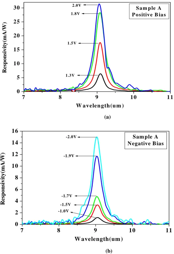
(3) Spectral Response
Figure 7 shows the spectral response of Sample A under different positive and negative biases. The responsivity is increased with the applied bias, and the lineshape of the photo response is unchanged. Only one peak at the long wavelength 9.05um is observed. This result is consistent with the transition of electrons from the top of the first miniband to the bottom of the second miniband. The maximum responsivity is about 31mA/W at wavelength 9.05um under bias +2.0V, and 15mA/W at wavelength 9.03um under bias -2.0V. The short wavelength absorption corresponding to the electron transitions from the bottom of the first miniband to the top of the
that the superlattice is no longer a low resistance structure and voltage drops on it. Th
appeared under high bias at high temperature because
th We also show the full width at the half
maximum (FWHM) in Fig. 8. The FW scattering in the superlattice is in
second miniband is disappeared. This phenomenon is because the doping density in superlattice is quite low so
erefore, the minibands may not be formed due to the misalignment of the energy states in the adjacent wells. Therefore, the wave function is localized. and the spectral responsivity becomes sharper [9].
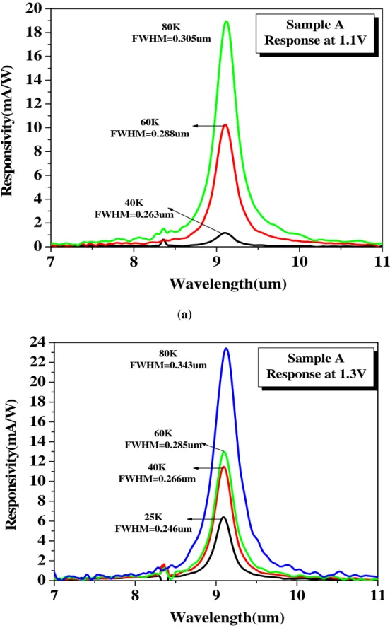
Figure 8 shows the spectral response of Sample A under biases +1.1V and +1.3V at several temperatures. When the temperature is increased, the carriers in the superlattice will increase by absorbing the thermal energy, and the superlattice becomes more conductive. Therefore, the external bias must be redistributed. The voltage drop on the superlattice is decreased, and more external bias drops on the blocking layers, as shown in Fig. 9. Under low bias, the responsivity is increased with the temperature because more voltage drops on the blocking barriers at high temperature. However, the response is dis
e dark current is also increased with temperature.
HM increased with temperature because the impurity creased.
Furthermore, the responsivity can be expressed as
g hc e
R(
λ
)=λ
η
, (1) where c is the velocity of light in the vacuum, g is the optical gain, andη
is the quantumefficiency which is the number of photoelectrons generated by per incident photon. With the sponsivity taken as 31mA/W under +2.0V, 15mA/W under -2.0V, and the optical gain taken as
ntum efficiency to be 0.43% at the voltage +2.0V and 0.21% at the vo
(4) Specific Detectivity
rce [10], and takes form as :
, (2) where is the dark current. So,
re
1, we estimated the qua ltage -2.0V.
We assume that the shot noise is the main current noise sou
f
eI
i
rms= 2
dΔ
dI
detectivity is derived as : d d i eI A R D 2 * = , (3)The peak detectivity D* at 60K is 3.7×10⁸cmHz1/2/W under V=1.1V at wavelength 9.1μm and 1.5×10⁸ cmHz1/2/W under V=1V at wavelength 9.12μm at 80K. The detectivity will be descreased as the temperature increasing. This result is caused by the rapidly increasing dark current.
(a)
(b)
Fig. 5 (a) The structure of Sample A (high doping density 1Ⅹ1017 ) and B (low doping density 5Ⅹ1016 ) (b) Their schematic energy band diagrams.
-3 -2 -1 0 1 2 3 1E-10 1E-9 1E-8 1E-7 1E-6 1E-5 1E-4 70K 70K Photocurrent C u rren t( A ) Voltage(V)
Fig. 6 The current-voltage curves of Sample A. The solid lines are the dark current at temperature 40Kto100K,while the dash line is the photocurrent at temperature 30K. The positive voltage means top contact is applied positive biases.
7 8 9 1 0 1 1 0 5 1 0 1 5 2 0 2 5 3 0 2 .0V 1.8V 1.5V 1 .3V S a m p le A P o sitiv e B ia s Responsivity(mA/W) W a v elen gth (u m ) (a) 7 8 9 10 11 0 2 4 6 8 10 12 14 16 -2.0V -1.9V -1.7V -1.5V -1.0V Sam ple A N egative Bias R es p on si vi ty(m A /W ) W avelength(um ) (b)
Fig. 7 The spectral response of Sample A measured (a) at several positive biases and (b) at several negative biases.
7
8
9
10
11
0
2
4
6
8
10
12
14
16
18
20
80K FWHM=0.305um 60K FWHM=0.288um 40K FWHM=0.263um Sample A Response at 1.1VR
esp
o
n
si
v
it
y
(m
A
/W
)
Wavelength(um)
(a)7
8
9
10
0
2
4
6
8
10
12
14
16
18
20
22
24
11
Sample A Response at 1.3V 80K FWHM=0.343um 60K FWHM=0.285um 25K FWHM=0.246um 40K FWHM=0.266umR
esp
o
n
si
v
it
y
(m
A
/W
)
Wavelength(um)
(b)Fig. 8 The spectral response of Sample A (a) under bias +1.1V and (b) under bias +1.3V at several temperatures.
(a)
(b)
Fig. 9 The band diagrams under a positive bias : (a) At the low temperature. (b) At the high temperature, the voltage drop on the superlattice becomes lower, and the voltage drop on the blocking layers becomes higher.
2. SLIP with Doping Density 5Ⅹ10
16in the Superlattice
(1) Sample Structure and Band DiagramIn order to see the effect of different doping density in the superlattice, the Sample B is designed as the same as Sample A except the doping density (5x1016 cm-3) in the superlattice. Therefore, the band diagram of Sample B is also the same as Sample A (as shown in Fig. 5).
(2) Current-voltage Characteristic
The I-V curves of Sample B under different temperatures are shown in Fig. 10. The solid lines present the dark current at 40Kto100K,while the dash line is the photocurrent at 30K under the room temperature background radiation upon the detector. According to the I-V curves, we observe the background limited performance temperature TBLIP is up to 70K. The dopant
migration can also be observed in Sample A.
(3) Spectral Response
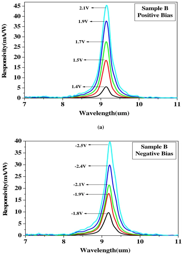
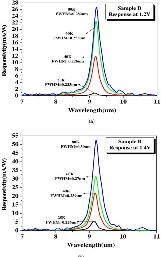
The spectral response of Sample B under several positive and negative biases is shown in Fig.11. The peak responsivity is about 45.4mA/W under +2.1V, at wavelength 9.15um and 40mA/W under -2.5V, at wavelength 9.21um.
Figure 12 shows the spectral response of Sample B under biases +1.2V and +1.4V at several temperatures. The reason that the responsivity of Sample B is increased with temperature is the same as Sample A. When the temperature increases, the external bias must be redistributed. The voltage drop on the blocking barriers is increased, and the response becomes larger than that at low temperature. We can also see that the FWHM of Sample B is increased with temperature.
With the responsivity taken as 45.4mA/W under +2.1V, and 40mA/W under -2.5V, we estimated the quantum efficiency to be 0.62% at the voltage +2.1V and 0.54% at the voltage -2.5V.
(4) Specific Detectivity
The peak detectivity D* at 60K is 2.44×10⁹cmHz1/2/W under +1.2V at wavelength 9.19μm, and 9.44×10⁸cmHz1/2/W under +1.4V at wavelength 9.20μm at 80K. The detectivity will be descreased as the temperature increasing. This result is caused by the rapidly increasing dark current.
3. Comparison of Sample A and Sample B
In order to compare the performance of Sample A (high doping density 1x1017cm-3) and
Sample B (low doping density 5x1016cm-3), we summarized those experimental results for
analysis. Figure 13 shows the I-V curves under different temperatures. The solid lines are the dark current at 60Kand 70K,while the dash line is the photocurrent at 30K. Because the doping density in the well in Sample A is higher than that in Sample B, the dark current and photocurrent of Sample A are higher than Sample B. However, the background limited
performance temperature TBLIP of Sample B (70K) is larger than that of Sample A (60K).
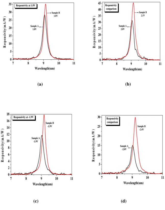
We also show the responsivity comparison in Fig. 14. Sample B has better responsivity for both forward and reverse biases than Sample A. This may be due to the impurity scattering in the well. When the electrons are excited by the photons into the second miniband, and oscillate between two blocking layers, these electrons will be scattered by the impurities in the wells into the first miniband, and emit the LO phonons. It is expected that the absorption rate of photons and the scattering rate of electrons in the superlattice are both proportional to the doping density in the well. Their effects on the photocurrent will cancel each other. According to our experimental results, the device with low doping density is better than the high doping density one because of the decrease of impurity scattering.
The operational voltage of Sample A ranges from 1.3V to 2.0V, under forward bias and from -0.9V to -2.0V under reverse bias. The operational voltage of Sample B ranges from 1.3V to 2.2V under forward bias, and from -1.7V to -2.5V under reverse bias. Because the voltage drop in the superlattice of Sample B is higher than Sample A, the operational voltage of Sample B is higher than Sample A.
Sample B has better quantum efficiency under both forward and reverse biases than Sample A.
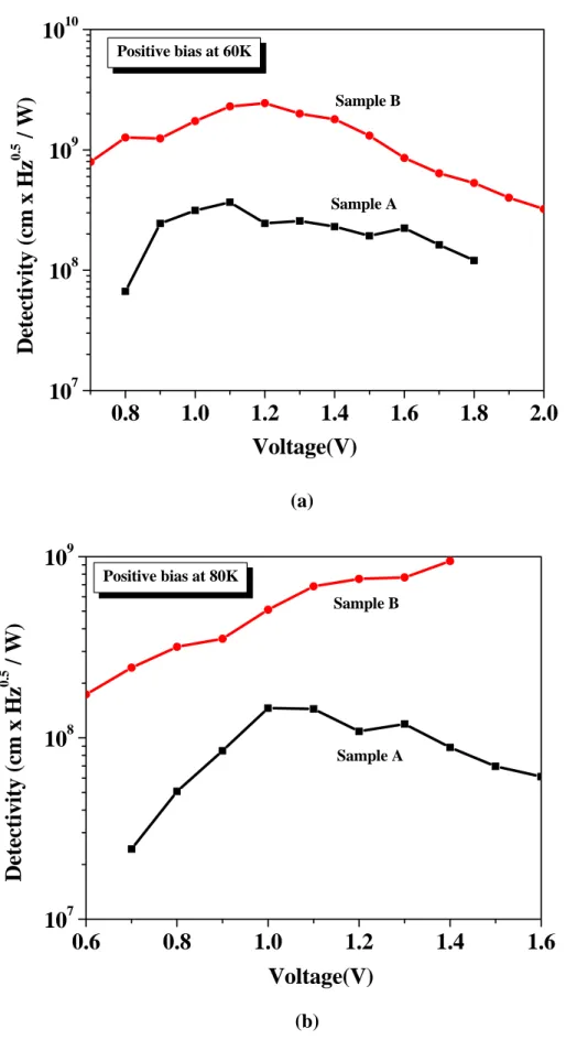
The detectivity of Sample A and B under several positive biases at 60K and at 80K are shown as Fig. 15. The detectivity of Sample A is lower than Sample B at 60K and 80K.
As a consequence, Sample B (doping density 5x1016cm-3) has better background limited
performance temperature TBLIP,responsivity, quantum efficiency, and detectivity.
-3
-2
-1
0
1
2
3
1E-10
1E-9
1E-8
1E-7
1E-6
1E-5
1E-4
70K
photocurrent
70K
Cu
rren
t(A)
Voltage(v)
Fig. 10 The current-voltage curves of Sample B. The solid lines are the dark current at temperature 40Kto100K,while the dash line is the photocurrent at temperature 30K.
11 7 8 9 10 0 5 10 15 20 25 30 35 40 45 2.1V 1.9V 1.7V 1.5V 1.4V Sample B Positive Bias R esp o n si v it y (m A /W ) Wavelength(um) (a) 7 8 9 10 0 5 10 15 20 25 30 35 40 11 -2.5V -2.4V -2.1V -1.9V -1.8V Sample B Negative Bias R es p on si vi ty( m A /W ) Wavelength(um) (b)
Fig. 11 The spectral response of Sample B measured (a) at several positive biases and (b) at several negative biases.
11
7
8
9
10
0
2
4
6
8
10
12
14
16
18
20
22
24
26
28
80K FWHM=0.282um 60K FWHM=0.255um 40K FWHM=0.226um 25K FWHM=0.223um Sample B Response at 1.2VR
esp
o
n
si
v
it
y
(m
A
/W
)
Wavelength(um)
(a)7
8
9
10
11
0
5
10
15
20
25
30
35
40
45
50
55
80K FWHM=0.30um 60K FWHM=0.27um 40K FWHM=0.239um 25K FWHM=0.226um Sample B Response at 1.4VR
esp
o
n
si
v
it
y
(m
A
/W
)
Wavelength(um)
(b)Fig. 12 The spectral response of Sample B (a) under bias +1.2V and (b) under bias +1.4V at several temperatures.
-3
-2
-1
0
1
2
3
1E-10
1E-9
1E-8
1E-7
1E-6
1E-5
1E-4
I-V comparison Sample A 60K Sample A Photocurrent Sample A 70K Sample B 60K Sample B 70K Sample B PhotocurrentC
u
rren
t(A)
Voltage(V)
Fig. 13 The I-V curves of Sample A and B. The solid lines are the dark current at temperature 60Kand 70K,while the dash line is the photocurrent at temperature 30K.
7 8 9 10 11 0 5 10 15 20 25 30 35 Sample A 1.8V Sample B 1.8V Responsivity at 1.8V R esp o n si v it y (m A /W ) Wavelength(um) 7 8 9 10 11 0 5 10 15 20 25 30 35 40 45 Sample A 2.0V Sample B 2.1V Responsivity comparison R es p on si vi ty (m A /W ) Wavelength(um) (a) (b) 7 8 9 10 11 0 2 4 6 8 10 12 14 16 18 Sample A -1.9V Sample B -1.9V Responsivity at -1.9V R esp o n si v it y (m A /W ) Wavelength(um) 7 8 9 10 11 0 5 10 15 20 25 30 Sample A -2.0V Sample B -2.4V Responsivity comparison R es p on si vi ty( m A /W ) Wavelength(um) (c) (d)
Fig. 14 The spectral response comparison. Sample B has better responsivity for both forward and reverse biases than Sample A.
0.8
1.0
1.2
1.4
1.6
1.8
2.0
10
710
810
910
10 Positive bias at 60K Sample B Sample AD
etectivity (cm
x
H
z
0.5/ W
)
Voltage(V)
(a)0.6
0.8
1.0
1.2
1.4
1.6
10
710
810
9 Positive bias at 80K Sample B Sample AD
etectiv
ity (c
m
x
H
z
0. 5/ W
)
Voltage(V)
(b)Fig. 15 The detectivities of Sample A and B under several positive biases (a) at 60K and (b) at 80K.
4. 1-D Detector Array
In the section, we will show some experimental results of 1-D detector array. The sample structure is the same as Sample A (as shown in Fig. 5). New process for 1-D array is used, so some fabrication results are proposed first.
(1) Fabrication Result
Figure 16 shows the SEM picture of the trench with the optical isolation structure which is fabricated by PECVD deposition silicon nitride (Si3N4) and sputtering titanium (Ti) on the wall of
the trench. It is noted that the thicknesses of the Si3N4 and Ti on the wall are about 1500Å and
400Å when the deposition thickness is 2000Å on the top surface of the sample. Because the skin depth of Ti at the wavelength 9um is about 300Å, so we sputter thickness 5000Å on the top surface of the sample and thickness 1000Å on the wall of the trench to ensure that light would be reflected by the metal-insulator-semiconductor (MIS) structure.
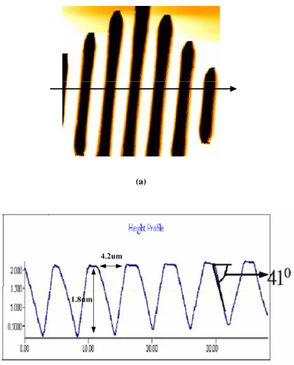
In order to couple the normal incident light, the V-groove coupling scheme is fabricated. Figure 17 shows the AFM picture of several V-grooves, and the tilted angel is about 41o. These facets can direct the normal incident light into the device though refraction, as shown in Fig. 18 (a). In order to analyze the couple efficiency of different tilted angles, we assume the incident light is TM mode and calculate the electrical field ratio of the refraction component to the incident light versus the tilted angle. The result is shown in Fig. 18 (b). We can see that the electrical ratio is 34.3% when the tilted angle is 41o. The maximum is 39.5% if the tilted angle is 54o. Finally, the fabricated detector array is shown in Fig. 19.
(2) Current-voltage Characteristic
Fig. 20 shows the I-V curves of 1-D detector array under different temperatures. The solid lines present the dark current from 20Kto80K,while the dash line is the photocurrent at 25K under the room temperature background radiation upon the detector. The dark current begins to dominate when temperature is above 50K. The background limited performance temperature TBLIP is up to
50K for the forward bias smaller than 1.4V, and reverse bias smaller than 1.3V.
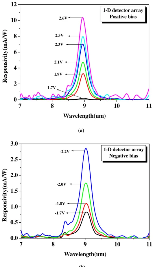
(3) Spectral Response
The spectral response of 1-D detector array under several positive and negative biases is shown in Fig. 21. The peak responsivity is about 10.3mA/W under +2.6V, at wavelength 8.95um and 2.85mA/W under -2.2V, at wavelength 9.03um.
With the responsivity taken as 10.3mA/W under +2.6V, and 2.85mA/W under -2.2V, we estimated the quantum efficiency to be 0.14% at the voltage +2.1V and 0.04% at the voltage -2.5V.
(4) Specific Detectivity
The peak detectivity D* at 60K is 8.02×10⁸cmHz1/2/W under +1.5V at wavelength 9.02μm, and 2.15×10⁸cmHz1/2/W under 1.4V at wavelength 9.04μm at 80K. The decrease of detectivity with
the increase of temperature is caused by the rapid increasing dark current.
Fig. 16 The SEM picture of the trench with the PECVD deposition Si3N4 and sputtering Ti on
the wall of the trench. The thicknesses of the Si3N4 and Ti on the wall are about 1500Å
and 400Å when the deposition thickness is 2000Å on the top surface of the sample.
5. Comparison of Single Device and 1-D Detector Array
In order to analyze the performance of 1-D detector array, we summarized experimental results. Figure 22 shows the I-V curves under different temperatures. The solid lines are the dark current, while the dash line is the photocurrent at 30K. We can observe both the dark current and photocurrent of single device are higher than detector array. This may be contributed that the contact resistance of the detector array is much higher than the single device. As shown in Figure 18(c), the area of the detection pixel is 45×45um2, and the contact is a metal ring which thickness is about 1um. It may make the higher contact resistance and lower current density. In order to make sure that the contact area will affect the current density, we apply silver on the detection pixel to increase the contact area. Figure 23 shows the I-V curves of the device which have Ag on the detection pixel or not. We can see that the current density of the device with Ag is much larger than the device without Ag. As a consequence, the higher contact resistance is caused by the small contact area.
Next, we show the comparison of spectral response in Fig. 24. The single device has better responsivity for both forward and reverse biases than the 1-D detector array. Besides the higher contact resistance of the detector array, the efficiency of V-grooves coupling scheme is another factor that affects the spectral response.
The detectivities of single device and 1-D array under several positive biases at 60K and 80K is shown in Fig. 25. Although the response of single device is larger than detector array, the detectivity of the single device is lower than detector array at 60K and 80K. This is because the dark current of single device is much higher than that of the detector array.
(a)
(b)
Fig. 17 The AFM picture of several V-grooves : (a) the original pattern, and (b) the profile of the AA’ direction. The tilted angel is about 41o.
(a)
(b)
Fig. 18 (a) The optical path of normal incident light into the device though refraction (b) The electrical field ratio of the refraction component to the normal incident light versus the tilted angle.
(a)
(b)
(c)
-2 -1 0 1 2 1E-12 1E-11 1E-10 1E-9 1E-8 1E-7 1E-6 1-D detector array 50K photocurrent 50K Curren t(A) Voltage(v)
Fig. 20 The current-voltage curves of 1-D detector array. The solid lines are the dark current at temperature 20Kto80K,while the dash line is the photocurrent at 25K.
7
8
9
10
11
0
2
4
6
8
10
12
2.6V 2.5V 2.3V 2.1V 1.9V 1.7V 1-D detector array Positive biasRe
spo
n
sivity
(m
A/W
)
Wavelength(um)
(a)7
8
9
10
11
0.0
0.5
1.0
1.5
2.0
2.5
3.0
-2.2V -2.0V -1.8V -1.7V 1-D detector array Negative biasR
esp
onsivity(m
A
/W
)
Wavelength(um)
(b)Fig. 21 The spectral responsivity of 1-D detector array measured (a) at several positive biases and (b) at several negative biases.
-3
-2
-1
0
1
2
3
1E-13
1E-12
1E-11
1E-10
1E-9
1E-8
1E-7
1E-6
1E-5
Single 60K Single Array 50K ArrayCu
rren
t(A)
Voltage(V)
Fig. 22 The I-V curves of single device and 1-D detector array. The solid lines are the dark current,while the dash line is the photocurrent at temperature 30K.
Fig. 23 The dark currents of 1-D detector array which have Ag on the detection pixel or not. The current density of the device with Ag is much larger than the device without Ag.
-3
-2
-1
0
1
2
3
10
-111x10
-101x10
-91x10
-81x10
-71x10
-61x10
-51x10
-41x10
-3 70K no Ag 70K have Ag 30K have Ag 30K no AgC
u
rren
t(A
)
Voltage(V)
7 8 9 10 11 0 2 4 6 8 10 12 14 16 18 Array 2.0V Single 1.5V Responsivity comparison R es p on si vi ty( m A /W ) Wavelength(um) 7 8 9 10 11 0 5 10 15 20 25 30 Array 2.6V Single 2.0V Responsivity comparison R esp o n si v it y (m A /W ) Wavelength(um) (a) (b) 7 8 9 10 11 0 1 2 3 4 5 Array -1.8V Single -1.7V Responsivity comparison R esp o n si v it y (m A /W ) Wavelength(um) 7 8 9 10 11 0 2 4 6 8 10 12 Array -2.2V Single -1.9V Responsivity comparison R esp o n si v it y (m A /W ) Wavelength(um) (c) (d)
Fig. 24 The spectral response comparison. Single device has better responsivity for both forward and reverse biases than 1-D detector array.
.2
0.8
1.0
1.2
1.4
1.6
1.8
2.0
2
10
710
810
9 Positive bias at 60K 1-D Array Single deviceD
etectivity (cm
x
H
z
0.5/ W
)
Voltage(V)
(a)0.8
1.0
1.2
1.4
1.6
10
710
810
9 Positive bias at 80K 1-D Array Single deviceD
etectivity (cm
x
Hz
0. 5/ W
)
Voltage(V)
(b)Fig. 25 The detectivities of single device and 1-D array under several positive biases (a) at 60K and (b) at 80K.
D. 結論與計畫自評
In the report, we discuss the effect of doping density in the superlattice with the comparison of the experimental results of Sample A (high doping density 1Ⅹ1017) and Sample B (low doping density 5Ⅹ1016). Besides, we also develop a fabrication process of 1-D detector array for the thermal imaging application.
From the I-V curves, the dark current and photocurrent of Sample A are larger than those of
Sample B, and the background limited performance temperature TBLIP of Sample B (70K) is
higher than Sample A (60K).
Next, we summarize the spectral response. Sample B has better responsivity for both forward and reverse biases than Sample A. It may be attributed to the impurity scattering in the well. The absorption rate of photons and the scattering rate of electrons are both proportional to the doping density in the well, and their effects on the photocurrent cancel each other. As a result, Sample B has better responsivity, and quantum efficiency. It is concluded that the performance of Sample B (low doping density 5x10¹⁶) is better than Sample A (high doping density 1x10¹⁷) due to the decrease of the impurity scattering.
The fabrication process of 1-D detector array is illustrated and investigated. In the process, the V-groove couple scheme is used instead of the edge couple one, and the optical isolation formed by metal-insulator-semiconductor (MIS) structure is used to prevent the crosstalk between the detection pixels. Each step of the process is investigated and then integrated into the complete fabrication process. The experimental results of the fabricated 1-D detector array are also proposed to analyze the performance.
The peak responsivity of 1-D detector array is 10.3mA/W at the voltage +2.6V, which is smaller than sample A (31mA/W under bias +2.0V). The dark current of detector array is much smaller than single device. This may be due to the higher contact resistance of detector array.
In the future, we will improve the process of 1-D detector to increase the contact area of metal ring for lower contact resistance and larger tilted angle for better couple efficiency. It will be a new method to fabricate 1-D detector for thermal imaging applications.
E. 參考文獻
[1] Ralph E. Williams, “Gallium Arsenide Processing Techniques,” published by the Artech House Microwave Library, copyright 1984.
[2] “Gallium Arsenide Materials, Devices, and Circuits,” edited by M. J. Howes and D.V. Morgan (1985).
[3] D.W. Shaw, J. electrochem. Soc., Vol. 128, No.4, 874-880, 1981.
[4] C. J. Chen, K. K. Choi, M. Z. Tidrow, and D. C. Tsui, Appl. Phys. Lett. 68, 1446, 1996.
[5] K.K. Choi “The Physics of Quantum Well Infrared Photodetectors”, Published by World Scientific.