多層印刷電路板地彈雜訊問題研究
計畫類別: 個別型計畫
計畫編號: NSC93-2213-E-009-096-
執行期間: 93 年 08 月 01 日至 94 年 07 月 31 日
執行單位: 國立交通大學電信工程學系(所)
計畫主持人: 吳吳
計畫參與人員: 曾智雄,陳怡龍,邱培銘
報告類型: 精簡報告
處理方式: 本計畫可公開查詢
中 華 民 國 94 年 10 月 30 日
Abstract—Power bus structure, consisting of two parallel solid power and ground planes separated by an insulator, behaves as a cavity resonator at high frequencies. Noise on the power bus, due to a sudden change in the current drawn by active component, can appear as an undesired spatial fluctuation in the voltage between power and ground, especially at resonant frequencies of the resultant cavity, which may lead to problems in signal integrity, excessive delays, false switching, and radiated emission. These resonances can be suppressed by introducing high-frequency loss into the structure. This paper investigates a simple method to reduce self/transfer impedance of power-ground planes for mitigating power/ground bounce in high speed printed circuit board (PCB) design by adding a thin layer of magnetic material coating to the inside-facing surfaces of copper power and ground plates to increase their effective high frequency surface impedance. The increased surface impedance will increase the attenuation constant of the propagating wave inside the cavity that benefits reduction of cavity’s quality factor (Q factor). The simulation results obtained from a modified cavity resonator model show that increasing surface impedance can dramatically reduce self and transfer impedances at board resonant frequencies.
Index Terms—cavity resonator model, ground bounce,
magnetic material coating, self/transfer impedance, SSN, surface impedance.
I. INTRODUCTION
N the so-called simultaneous switching noise (SSN) or ground bounce problem, any sudden surge of the current drawn by active devices from power-ground planes at one point can cause voltage fluctuation at any other point across the entire PCB that is directly proportional to the transfer impedance between the two. As a closely-spaced parallel plane pair forms a high-Q cavity resonator, extremely high transfer impedance peaks can occur at resonance frequencies. With the operating frequency exceeding 1 GHz and working voltages continuing to decrease for reducing power dissipation in high-speed digital circuits, noise in the power distribution system has become a major performance-limiting problem.
Manuscript received July 9, 2004; revised January 10, 2005. This work was supported by the National Science Council, Taiwan, R.O.C., under Grant NSC93-2213-E-009-096.
The authors are with the Institute of Communication Engineering, National Chiao Tung University, Hsinchu, Taiwan 300, R.O.C (e-mail: [email protected]).
To avoid SSN or ground bounce, the power distribution systems are required to have low impedance across a broad bandwidth. Some commonly used mitigation techniques for controling board noise are: (1) added discrete decoupling capacitors between power and ground planes, (2) enhanced embedded capacitance, i.e., the natural capacitance between power and ground planes, to provide better decoupling [2]-[4], (3) added dissipative termination along the board edges to reduce the resonance peaks [5], and (4) added additional loss including dielectric, conduction, component, and/or radiation losses to damp board resonance [6], [12].
Discrete decoupling capacitors are employed to mitigate SSN noise in PCB design. Traditionally, equivalent series resistance (ESR) of decoupling capacitors are chosen to be small for providing low impedance at high frequency but the existence of series inductance will reduce the effectiveness of decoupling capacitors. Their effective frequency range is limited by intrinsic inductance of capacitor and extrinsic inductance including lead and interconnection (e.g., mounting pads, traces and vias) inductances. At frequencies above its series resonance frequency, the increasingly higher inductive reactance defeats the purpose of low-impedance decoupling. Then, decoupling capacitors with small ESR will result in higher Q factor and impedance peak at board resonant frequencies. In addition, use of large number of decoupling capacitors consumes the valuable board area and reduces the reliability of PCB.
Xu and Hubing exploited the concept of enhanced “embedded” capacitance by using a thin dielectric layer between the solid power and ground planes to effectively increase the influence of solid planes’conduction loss on damping board resonances [2]-[4]. If the spacing between the two solid planes is on the order of conductor’s skin depth, conductor loss becomes quite effective in reducing resonant impedance peak. For this to happen, however, the substrate used need to be extremely thin. This thin dielectric layer may present difficulty in board fabrication, for instance, vias through this thin layer may short the power and ground planes together. Novak used dissipative edge termination to reduce board resonances [5]. Dissipative components placed along the edges of the board are designed to present load impedance matched to that of the impinging wave such that, ideally, no wave will be reflected back into the parallel-plate region. Without reflection wave, standing wave can not be formed, board resonance is thus
A Theoretical Investigation of the Resonance
Damping Performance of Magnetic Material
Coating in Power/Ground Plane Structures
Lin-Kun Wu, Member, IEEE and Chih-Hsiung Tseng
prevented. Therefore, in principle, the board becomes an infinitely-large parallel-plate radial waveguide. As the component spacing has to be much smaller than the shortest wavelength of concern, however, a large number of dissipative components may be needed which will limit its use in practical applications.
To avoid transfer impedance peaks appearing at board resonant frequencies, we can introduce additional loss into the board to reduce its Q factor. This may include increasing dielectric, conduction, component, and/or radiation losses. Generally, dielectric loss is kept small to provide good isolation and avoid leakage current between power and ground planes. The radiation loss from board edges, which behave as slot antennas, is proportional to the square of spacing between the two planes. In practice, the spacing is on the order of 10 mils on PCBs, therefore radiation loss is minor compare to other losses and can be neglected.
Recently, decoupling capacitors with purposely increased ESR have also been proposed to suppress board resonances. Zeff and Hubing suggested applying such lossy components to reduce the impedance at board resonant frequencies [6]. Resistive components mounted between the power-ground pair can reduce the resulting cavity’s Q factor and impedance peak at resonant frequencies. Novak et al. suggested using distributed matched bypassing (DMB) method to create a smooth impedance profile [12]. The DMB is implemented by annular resistive interstitial element screened-in (ARIES) that is based on the annular buried resistor (ABR). Printed resistors are inserted only at one of the capacitor terminals connecting the power plane for reducing the number of required components. The direct physical connection of the printed resistor can also decrease interconnection inductance.
In a design note, Johnson mentioned the idea of applying a thin coating of steel to the inside-facing surfaces of a power and ground plane pair to damp its resonances [7]. In this paper, a theoretical investigation of the potential performance of such a concept is reported. Surface impedance is incorporated into the
well-known cavity model in part A of Section II to model the effect of conductor loss. In order to increase high-frequency conductor loss, the 2-metallic-layer structure constituted of a thin magnetic material coated on one side of the copper plate is then considered in part B of Section II. For a better understanding of the relationship between the loss factor and impedance peak at resonance, the Q factor of cavity, including the effects of dielectric and conductor losses, is derived in part C of Section II. Theoretical results obtained for various coating thicknesses and material properties are used to evaluate the potential resonance damping performance of the proposed concept. Numerical results and discussions are presented in Section III, which is followed by conclusions in Section IV.
II. METHOD OF ANALYSIS
A. Cavity Resonator Model
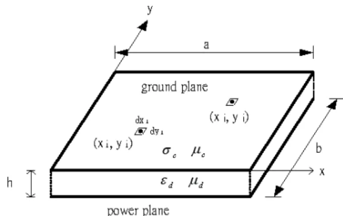
The rectangular parallel plane pair shown in Fig. 1 is consisted of two solid planes of the same size a × b separated by a dielectric of thickness h. It is assumed that dielectric thickness is much smaller than a, b, and the wavelength (of the highest frequency of interest. Under this assumption, radiation loss from board edges can be ignored. Therefore, this structure can be modeled as a TMzcavity with two electric conductor planes representing the power and ground, and each side of the rectangular board approximated as a perfect magnetic conductor. The ports i and j are respectively located at (xi, yi) and (xj, yj) with rectangular cross section of size dxi× dyiand dxj × dyjwhich are much smaller than the shortest wavelength of interest. The transfer impedance is given by [1]-[5]
) 2 ( sinc ) 2 ( sinc ) cos( ) cos( ) 2 ( sinc ) 2 ( sinc ) cos( ) cos( ) ( 0 0 2 2 2 2 j yn j xm j yn j xm i yn i xm i yn i xm m n xm yn mn ij dy k dx k y k x k dy k dx k y k x k k k ab h j Z
(1a) 0 0 0 0 0 , , , 4 2 1 2 n m n or m n m b n k a m kxm yn mn (1b)where m and n are indices of the cavity’sTMzmodes. The complex propagation constantof the parallel plane pair with imperfect conductor and dielectric can be expressed as
j j h Z j j d s d d [1 2 ][1 tan ] (2a) where ] 2 ) ( tan sin[ ) ( 1 4 1 2 2 R X X R d d (2b) ] 2 ) ( tan cos[ ) ( 1 4 1 2 2 R X X R d d (2c)
tan 2 2 1 h R h X R d s d s (2d) tan 2 tan 2 h X h R X d s d s (2e)
In (2), Rsand Xsare respectively the real and imaginary parts of the surface impedance Zsof the conductor, andd,d, and tan represent the permeability, permittivity, and loss tangent of the dielectric, respectively. For numerical calculation, the infinite summation must be truncated; in this study, the maximum m and
n used are 1000 respectively, to achieve a 5% maximum error at
all resonant frequencies [2].
Since the imperfect dielectric and conductor introduce non-zero attenuation constant, radial wave is thus attenuated as it propagates away from its source of excitation (i.e., the transient current flowing along the power/ground vias) and reflects back from the board edges. Therefore, coupling between different board locations is reduced and board’s resonant behavior is suppressed. For good dielectric and conductor (i.e., tan,Rs/(dh) and Xs/(dh)and Rs
Xs at high frequency), R in (2d) approaches 1 while X in (2e) approaches Rs/(dh) + tan, which increases as substrate thickness decreases. As a result,increases when h decreases, this concept has been presented in [2]-[4]. Alternatively, (2d) and (2e) also show that R and X, and therefore, can be made larger by simply increasing the surface impedance of the conductor, this concept is explored further here.B. Surface Impedance of a Copper Plate Coated with a Thin Magnetic Material
As mentioned above, we can increase surface impedance to enhance attenuation constant for suppressing board resonances. In order to increase surface impedance, the inside-facing surfaces of the copper power and ground plates are each coated with a thin layer of magnetic material. The surface impedance of the composite 2-metallic-layer structure is derived first.
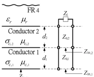
Fig. 2 shows that an infinite plane conductor with
conductivity c1, permeabilityc1and thickness d1 is coated over another conductor of conductivityc2, permeabilityc2and thickness d2, which is backed by a FR-4 substrate of infinite thickness. For a TMz wave between the parallel-plate conductors with a very large but finite conductivity, the electromagnetic field will penetrate conductor and incur power loss in the plates [13]. This necessitates the presence of a non-vanishing axial electric field at the plate surfaces and, therefore, the penetrating field can be regarded as a plane wave normally incident onto each conductor plate. Then, the surface impedance of an imperfect conductor, which is the ratio of axial electric field to surface current density accompanying the transverse magnetic field, can also be treated as the input impedance looking into the conductor plate. Consider a plane wave normally incident onto the lower side of conductor 1, the effective surface impedance of the composite structure can be obtained as Zin,1from the equivalent transmission line model shown in Fig. 2 in which characteristic impedances Z0,1and Z0,2 are the same as the intrinsic impedance of each of the two conductors (i.e.,c,1andc,2). From transmission line theory,
conductor 2 can be treated as a transmission line of length d2, the input impedance Zin,2 looking into conductor 2 from
conductor 1 is expressed as ) tanh( ) tanh( 2 2 2 , 0 2 2 2 , 0 2 , 0 2 , d Z Z d Z Z Z Z L L in (3)
where is the complex propagation constant of the propagating wave within conductor 2 and load impedance ZLis equal to the intrinsic impedancedof FR-4 substrate. Repeat this for the conductor 1 with Zin,2serves as its load impedance, the desired input impedance or the surface impedance of the composite structure can then be derived as
) tanh( ) tanh( 1 1 2 , 1 , 0 1 1 1 , 0 2 , 1 , 0 d Z Z d Z Z Z Z in in s (4)
For good conductor considered here, the various characteristic or intrinsic impedances and complex propagation constants appearing in (3) and (4) are given by
i c i c i c i f j Z , , , , 0 (1 ) , i = 1, 2 (5) i c i c i (1 j) f,, , i = 1, 2 (6)
When frequency approaches 0- and ∞-Hz, (4) reduces to (7a)
(7b) whereiis the skin depth, which is inversely proportional to the square root of frequency, of the i-th (i = 1 or 2) conductor. In (7a) the surface impedance of the composite structure is
) ( ) 1 ( ) ( 1 1 1 1 1 , 1 , 2 2 1 1 2 2 , 1 1 , d f j d and d d d Z c c c c d s
Fig. 2. Side view of the 2-metallic-layer and its equivalent transmission line model.
approximated as parallel connections of 3 resistors, i.e., each of the two conductor’s DC sheet resistance and intrinsic impedance of the FR-4 substrate. At low frequencies, withd being around 180for FR-4 and the twocd terms in the order of 100’s of S, 1/d term in (7a) can be ignored. At high frequencies when << d1, surface impedance is completely governed by conductor 1’s material properties. In between the
two extremes, behavior of Zsis quite complicated and can only be predicted by (4).
C. Quality Factor of Parallel-Plate Cavity
From circuit point of view, increasing loss can lower Q factor at resonance. To see how it happens, we follow the approaches used in [1]-[4] by rewriting (1) as
0 0 1 1 m n mn mn mn mnj mni ij R C j L j N N Z (8) where ) 2 ( sinc ) 2 ( sinc ) cos( ) cos( ) , ; , ( i yn i xm i yn i xm mn i i i i mni dy k dx k y k x k dy dx y x N ) 2 ( sinc ) 2 ( sinc ) cos( ) cos( ) , ; , ( yn j j xm j yn j xm mn j j j j mnj dy k dx k y k x k dy dx y x N h h R h X ab C d s d s d mn ) tan 2 2 1 ( ) ( 2 2 ym xm d mn k k ab h L ) 2 tan tan 2 ( h X h R ab h R d s d s d mn The resonant frequency and the Q factor of each mode are given by d d d s d s d s d s ym xm mn h R h X h R h X k k f 2 ) tan ( ) tan ( 2 2 2 (9) tan 2 tan 2 tan 2 2 1 h X h R h R h X C R Q d mn s d mn s d mn s d mn s mn mn mn mn (10)
It appears that Cmn, Rmn, fmn, and Qmnare all functions of Rs, Xs,
tan,and h. For good conductor and dielectric, the third term
inside the parenthesis associated with Cmnand Rmnexpressions is much smaller than the corresponding first two terms and can be ignored. Similarly, Rstan/dh << Xs/dh inside the fmn expression. Thus, as Zs increases, Cmn is increased, Rmn is decreased, and fmnis slightly decreased from the lossless case. Based on the same reasoning, the third term of both the numerator and denominator of Qmncan be ignored to result in the following approximation
d c d mn s mn Q Q h R Q 1 1 1 tan 2 1 (11)
where the Q factors due to conductor loss (Qc) and dielectric loss (Qd) are given by Qcmndh/(2Rs) andQd1/tan.
III. RESULTS AND DISCUSSIONS
As mentioned earlier, an effective solution for mitigating power/ground bounce is to reduce board impedance. It can be achieved by adjusting parameters of dielectric and conductor plate. The effect of substrate thickness is considered first. Next, the effect of the magnetic material coating on surface impedance is discussed. Finally, the influence of magnetic material coating on board impedance is analyzed.
A. Effects of Substrate Thickness on Self/Transfer Impedances and Q Factor
According to (1), board impedance is proportional to the spacing between the two solid planes. Therefore, reducing the spacing can lower board impedance. Figs. 3(a) - (c) illustrate the self and transfer impedances and Q factor of a 15.6-cm by 10.6-cm test board consisting solely of copper power and ground plates of the same thickness 17.5 m (i.e., 1/2-Oz. copper), relative permeability 1 and conductivity 5.8 × 10⁷S/m,
which are separated by a FR-4 substrate with relative permittivity 4.4 and loss tangent 0.019.
Three different substrate thicknesses of 508-, 254-, and 101.6-m (i.e., 20-, 10-, and 4-mil) are considered. Simulation results clearly demonstrate that the thinnest test board has the lowest resonance impedance peaks and Q factors. As can be seen from (11), the thinner the substrate is, the lower the Qcand, therefore, Qmnare. On the other hand, (8) indicates that thinner substrate produces larger Cmn, smaller Rmn and Lmn and, therefore, lower Zijat all resonant frequencies.
B. Effects of Magnetic Material Coating on Surface Impedance
As discussed in the previous section, increasing surface impedance can enhance attenuation constant and decrease Q factor of the board. Traditionally, manufacturers of PCB use copper as the conductor plate due to its lower dc resistance. However, at high frequency, copper can not facilitate enough surface impedance to damp natural resonance of the board. The surface impedance of copper is compared with several common magnetic conductors in Fig. 4. The conductivity of copper, iron, cobalt, and nickel are 5.8-, 1-, 1-, and 1.4- × 107 S/m, and
relative permeability are 1, 4000, 600, and 250, respectively; here, for simplicity, conductivity and permeability are assumed to be frequency independent.
The two lower curves of Fig. 4 are for the two copper plates of thickness 17.5- and 35-m . They clearly demonstrate the effects of conductor thickness: (1) thinner conductor results in larger impedance at low frequencies, and (2) skin effect takes off at higher frequency with thinner conductor. When skin effect is fully developed, however, surface impedance depends only on material’s conductivity and permeability, but not on its
thickness. For the four different conductors having the same copper plate thickness of 17.5m, since impedances at low and high frequencies are respectively proportional to 1/ and ()1/2, Fig. 4 shows that ZS,Fe> ZS,Co> ZS,Ni> ZS,Cu.
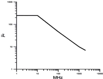
In above study, the relative permeability of magnetic material is assumed to be frequency independent. For real case, however, it will fall off rapidly and result in lower surface impedance as frequency increases. To evaluate the influence of frequency dependent permeability on the self/transfer impedance of board, an approximate model derived from data reported in [14] for the frequency-dependent permeability of nickel shown in Fig. 5 is considered. Consider the case of a 17.5m copper plate coated with a nickel layer of different thickness: 1-, 2-, and 4-m; the simulation results obtained from (4) for the surface impedance looking from the nickel side are shown in Fig. 6. As is predicted by (7), the resulting surface impedance is governed by copper’s DC sheet resistance at low frequencies, and by nickel’s surface impedance at high frequencies. In between, the transition region occurs at lower (higher) frequency range for thicker (thinner) nickel coating. As can been seen, a close look at (4) reveals that, since ZS,Niis much larger than ZS,Cu, the overall ZS can be simplified as ZS,Cu + ZS,Nitanh(NidNi), or ZS,Cu +
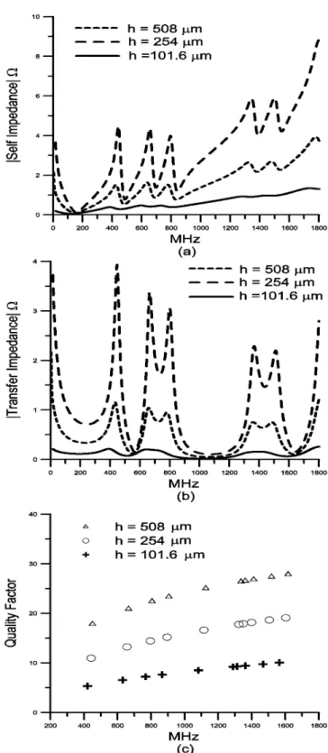
ZS,Ni(NidNi), at low frequencies. The transition region starts at a Fig. 3. (a) |Zii|, (b) |Zij|, and (c) Qmnof a 15.6 × 10.6 cm2copper power-ground
plane pair with three different substrate thicknesses. Port i is at (3.9 cm, 2.65 cm) and port j is at (11.7 cm, 7.95 cm).
Fig. 4. Surface impedance of copper and several magnetic metals.
frequency when the magnitude of the second term is comparable to that of the first term. Therefore, when nickel layer thickness increases, the starting frequency of transition region is decreased. For frequencies above 10 MHz, the surface impedance shown in Fig. 6 increases at a lower rate with increasing frequency due to the reduced relative permeability of nickel.
C. Effects of Magnetic Material Coating on Self/Transfer Impedances and Q Factor
The nickel-coated copper-plate whose surface impedance is larger than pure copper plane is then evaluated for its performance in reducing the self/transfer impedances of parallel plane pair. Consider a parallel pair of nickel-coated copper plates of 15.6-cm × 10.6-cm, where thickness is 17.5m for copper, 4m for nickel, and 101.6 m, 254 m and 508 m for different FR-4 substrate thickness. The simulation results are shown in Fig. 7. Compare with Fig. 3, the nickel-coated copper plate has a clear advantage in lowering self/transfer impedances and Q factor when frequency is higher than board capacitor’s
self resonant frequency of about 200 MHz
(
f
SR
1
/
2
(
L
ESLC
00)
1/2, where LESL is the equivalent series inductance of the board), because nickel-coating results in higher surface impedance and, therefore, higher attenuation constant. Below the first cavity resonant frequency (i.e.,f
10
458
MHz when losses are ignored), the impedance is mainly contributed by electrostatic capacitance, inductance and resistance of the board (i.e., C00, LESLand R00). In addition as evidenced by (9), increased surface impedance also results in lower board capacitor’s self-resonant frequency and cavity resonant frequencies.In Fig. 7(a), the self impedance increases with frequency as f > fSR. It can be explained by reviewing equivalent circuit parameters defined in (8). When operating frequency approaches each fmn, board impedance is mainly contributed by
Rmn and inductive reactance of the next higher-order mode.
Therefore, self impedance is primarily contributed by the inductive reactance, which increases with increasing frequency, since Rmnis reduced as surface impedance becomes larger. Fig. 6. Surface impedance of nickel-coated copper-plate with various
thickness of coating.
Fig. 7. (a) |Zii|, (b) |Zij|, and (c) Qmnof a 15.6 × 10.6 cm2nickel-coated copper
power-ground plane pair with three different substrate thicknesses. Port i is at (3.9 cm, 2.65 cm) and port j is at (11.7 cm, 7.95 cm).
IV. CONCLUSION
Cavity model was used to model the coupling behavior within a parallel plane pair, which behaves like a high Q cavity resonator. Its high resonance impedance peaks can result in serious ground bounce problem in high-speed PCBs. An effective approach to mitigate this problem is to reduce board impedance.
In this paper the concept of using a thin magnetic material coated over the inside-facing surfaces of conventional copper power and ground plane pair is investigated theoretically. The surface impedance model for the composite 2-layer structure is developed and used in the cavity resonator model for the computation of self and transfer impedances. Example calculations using a 4m-thick nickel as the coating material clearly demonstrate its effectiveness in damping high-frequency resonance impedance peaks with negligible effect on board’s DC resistance. The principle behind these is that the use of a thin magnetic material coating causes only a minimal change to the structure’s DC resistance (and, therefore, its low-frequency impedance), but significant increase to its high-frequency surface impedance. This results in much higher high-frequency conductor loss and attenuation constant, which in turn results in much lower resonance impedance peaks and Q factors. The theory developed here is easy to use, applicable for any magnetic material type and thickness, and layout independent.
REFERENCES
[1] T. Okoshi, Planar Circuits For Microwaves and Lightwaves, Munich, Germany: Springer-Verlag, 1985, pp. 10-42.
[2] M. Xu and T. H. Hubing, “Estimating the Power Bus Impedance of Printed Circuit Boards With Embedded Capacitance,”IEEE Trans. Adv.
Packag., vol. 25, no. 3, pp. 424-432, Aug. 2002.
[3] M. Xu, T. H. Hubing, J. Chen, J. L. Drewniak, T. P. Van Doren, and R. E. Dubroff, “Mitigating power bus noise with embedded capacitance in PCB designs,” in Proc. IEEE Int. Symp. Electromagn. Compat., Montreal, QC, Canada, Aug. 2001, pp. 487-489.
[4] M. Xu, T. H. Hubing, J.Chen, T. P. Van Doren, J. L. Drewniak, and R. E. DuBroff, “Power-Bus Decoupling With Embedded Capacitance in Printed Circuit Board Design,”IEEE Trans. Electromagn. Compat., vol. 45, no. 1, pp. 22-30, Feb. 2003.
[5] I. Novak, “Reducing Simultaneous Switching Noise and EMI on Ground /Power Planes by Dissipative Edge Termination,”IEEE Trans. Adv.
Packag., vol. 22, no. 3, pp. 274-283, Aug. 1999.
[6] T. M. Zeeff and T. H. Hubing, “Reducing Power Bus Impedance at Resonance with Lossy Components,”in Proc. EPEP’01 Conf., Boston,
MA Oct. 28-31, 2001.
[7] H. Johnson, “Steel-plated power planes,”EDN, March 21, 2002. [8] Z. L. Wang, O. Wada, Y. Toyota, and R. Koga, “An improved
closed-form expression for accurate and rapid calculation of power/ground plane impedance of multilayer PCBs,”Proc. of Symp. on Electromagnetic Theory, EMT-00-68, pp. 17-23, Toyama, Japan, Oct. 2000.
[9] Z. L. Wang, O. Wada, and R. Koga, “Modeling of Gapped Power Bus Structures for Isolation Using Cavity Modes,”IEEE Trans. Electromagn.
Compat., vol. 1, pp. 10-15, Aug. 2003.
[10] S. Chun, M. Swaminathan, L. D. Smith, J. Srinivasan, Z. Jin, and M. K. Iyer, “Modeling of Simultaneous Switching Noise in High Speed Systems,”IEEE Trans. Adv. Packag., vol. 24, no. 2, pp. 132-142, May 2001.
[11] J. C. Parker, Jr., “Via Coupling within Parallel Rectangular Planes,”IEEE
Trans. Electromag. Compat., vol. 39, no. 1, pp. 17-23, Feb. 1997.
[12] I. Novak, L. M. Noujeim, V. St. Cyr, N. Biunno, A. Patel. G. Korony, and A. Ritter “Distributed Matched Bypassing for Board-Level Power Distribution Networks,”IEEE Trans. Adv. Packag., vol. 25, no. 2, pp. 230-243, May 2002.
[13] S. Ramo, J. R. Whinnery, and T. V. Duzer, Fields and Waves in
Communication Electronics, 2nd ed., New York: Wiley, 1984, 288-305.
[14] R. M. Bozorth, Ferromagnetism, New York: IEEE Press, 1993, pp. 798-800.
Lin-Kun Wu (S’81–M’81)wasborn in Hsinchu,Taiwan,R.O.C.,in 1958. He received the M.S. and Ph.D. degrees in electrical and computer engineering from the University of Kansas, Lawrence, in 1982 and 1985, respectively.
From November 1985 to December 1987, he was a Post-Doctoral Research Associate at the Center for Research Inc., University of Kansas, where he was involved with microwave remote sensing and computational electromagnetics. In 1988, he joined the Department of Communication Engineering, National Chiao Tung University, Hsinchu, Taiwan, R.O.C., where he is currently a Professor. His current research interests include computational electromagnetics, biological effects and medial applications of electromagnetic energy, and electromagnetic compatibility.
Chih-Hsiung Tseng was born in Kaohsiung, Taiwan,
R.O.C., on July 8, 1974. He received the B.S. degree in Institute of Engineering, and System Science from National Tsing Hua University (NTHU), Hsinchu, Taiwan, R.O.C., in 1998, and the M.S degree in communication engineering from the National Chiao Tung University, Hsinchu, Taiwan, R.O.C, in 2000. He is currently working toward the Ph.D. degree.
His research interests include computational electromagnetics and the analysis and simulation of ground bounce in high-speed circuit design.