準光子晶體共振腔之WGM耦合特性探討
69
0
0
全文
(2) 準光子晶體共振腔之 WGM 耦合特性探討. 研 究 生:游嘉銘 指導老師:李柏璁. 教授. 國立交通大學光電工程系顯示科技研究所碩士班. 摘要. 在本論文中,我們藉由隨機調變兩種不同區域的晶格排列位置,來觀察十二對稱準 光子晶體中 WGM 模態對共振腔最內圍空氣孔洞的依賴度以及其對製程上的容忍度。接著 我們將實際元件製作出來並量測基本的雷射特性來驗證其結果。為了與 WGM 模態作比 較,在製程上,我們也製作具有隨機調變晶格位置的傳統三角形晶格排列的光子晶體。 藉由比較兩者的實際量測結果,我們可以更進一步的驗證 WGM 模態對共振腔最內圍空氣 孔洞的依賴度。. 接著我們將 WGM 模態擴展到十二對稱準光子晶體二重以及三重共振腔,並研究其中 的耦合特性以及基本的雷射特性。利用三維有限時域差分法我們可以計算準光子晶體二 重以及三重共振腔中的共振場圖和模態圖。最後,我們實際製作具有二重以及三重共振 腔的準光子晶體雷射, 並利用 micro-PL 的量測系統來量測基本的雷射特性。並將量測 的結果與模擬的結果比較分析。. ii.
(3) WGM Coupling Behavior of Two-Dimensional Quasi-Periodic Photonic Crystal Micro-Cavity. Student: Chia-Ming Yu Advisor: Prof. Po-Tsung Lee. National Chiao Tung University Department of Photonics & Display Institute. Abstract. We investigate and discuss the strong whispering gallery mode (WGM) mode dependence on inner-most air-holes of Dodecagonal quasi-periodic photonic crystal (DQPC) D2 (formed by 7 missing air-holes) micro-cavity and its fabrication tolerance by randomly varying the lattice of two separate regions. Hence, we design and fabricate DQPC micro-cavity lasers sustaining WGM. And we measure the basic lasing characteristic of two separate regions to verify WGM mode dependence. For comparison, we also fabricate traditional triangular PC D2 micro-cavity with the same lattice variation regions. From the results between DQPC D2 micro-cavity and PC D2 micro-cavity, we can verify the WGM mode dependence on the inner-most air-holes of DQPC D2 micro-cavity again.. Next, we extend the WGM mode in DQPC twin-cavity and triple-cavity. And we investigate the coupling behavior in these structures. We calculated resonance spectrum and resonance mode profiles of the DQPC twin and triple-cavity by 3D finite-difference time-domain (FDTD) method. And we fabricate the real device of DQPC twin and triple-cavity. The basic characteristics of DQPC twin and triple-cavity are measured by a micro-photoluminescence system. The measurement results are compared with the 3D FDTD simulation results.. iii.
(4) Acknowledgement 隨著這篇論文的完成,我也將卸下學生的身份,往我人生的下一階段邁進。兩年的 研究生生涯,現在回想起來,真的過得很快,轉眼間我已經要畢業離開學校。兩年的時 間,我學到很多也得到很多。很慶幸當初能夠進到 PTL 這個實驗室,實驗室的人都很好 相處,讓我這兩年的日子都過得很開心,也讓我能夠順利的完成碩士論文。. 能夠完成這篇論文,要感謝的人非常多。首先我要感謝我家人在我求學階段中,給 予我的支持與鼓勵。沒有你們,我可能沒辦法一路念到研究所畢業;因為你們,我才有 繼續堅持的動力。還有一路從大學陪我到研究所畢業的女朋友柏伶,在我人生遇到不順 遂或挫折的時候,幸好有你陪我度過並給我鼓勵,現在我要將畢業的喜悅與你分享。當 然還有實驗室的大家,首先謝謝指導教授李柏璁老師在這兩年中給予我的指導與意見。 還有負責帶我的博士班學長盧贊文,謝謝你時常提供我想法,並且幫我解答疑惑。另外 還有教我機台的蔡豐懋學長,畢業也不忘回來聊天打屁的蘇國輝、陳鴻祺、陳書志學長 以及張資岳、范峻豪學長,多虧你們才讓我們碩二這一年在作實驗之餘不至於太悶,也 希望實驗室烤肉出遊的這項傳統能夠一直延續下去。再來就是一起奮鬥成長的曾仲銓、 陳佳禾、陳思元、江俊德,感謝你們從碩一修課、碩二作實驗到最後寫論文時給我的意 見與鼓勵。最後也要感謝時常講沒營養笑話的鄉民代表:王明璽、施均融學弟,還有蔡 宜育、宋和璁學弟及時常陪我作實驗的林孟穎學妹,多虧你們才能讓實驗室時常處在歡 樂的氣氛並為實驗室增添的許多樂趣。當然還有很多曾經幫助過我的人,在此對各位獻 上由衷的感謝。. 2007/07 于新竹⎠ 國立交通大學. iv.
(5) Content Abstract (In Chinese)……….………………………………………………..…ii Abstract (In English)……………………………………………………………iii Acknowledgements……………………………………………………………..iv Content………………………………………………………………………….v List of Tables…………………………………………………………………...vii List of Figures…………………………………………………………...….…viii. Chapter 1. Introduction. 1.1.. Photonic Crystal…………………………………………………………..1. 1.2.. Microdisk Laser…………………………………………………………..7. 1.3.. Quasi-Periodic Photonic Crystal Laser………………………..………….8. 1.4.. An Overview of This Thesis…………..………………………………...10. Chapter 2. Simulation of Quasi-Periodic Photonic Crystal. 2.1.. Introduction……………………………………………………………...11. 2.2.. Finite-Difference Time-Domain Method………………………………..11. 2.3.. Device Structures………………………………………………………. 15. 2.4.. Simulation Results………………………………………………………17 2.4.1. WGM Mode Dependence……………………………..………….17 2.4.2. Quasi-Periodic Photonic Crystal Twin and Triple-Cavity……......20. 2.5.. Conclusion……………………………………………………………….25. v.
(6) Chapter 3. Fabrication of Membrane Structure Photonic Crystal Laser. 3.1. Introduction………………………………………………………...…….26 3.2. Fabrication of Two-Dimensional Photonic Crystal Laser……................26 3.2.1. Epitaxial Structure……………………………………………..……26 3.2.2. Dielectric Deposition………………………………………………..28 3.2.3. Photonic Crystal Patterns Definition………………………………..28 3.2.4. Patterns Transfer…………………………………………………….30 3.2.5. Substrate Undercut…………………………………………………..31 3.3.. Fabrication Results………………………………………………………33 3.3.1. Photonic Crystal with Random Lattice Variation….………………..33 3.3.2. Quasi-Periodic Photonic Crystal Twin and Triple Cavity…………..34. 3.4.. Conclusion……………………………………………………………….35. Chapter 4. Measurement Results. 4.1. Measurement Setup ……………………………………………………...37 4.2. WGM Mode Dependence…………………………………….………..…38 4.3. Basic Lasing Characteristics of Twin and Triple-Cavity……………..….45 4.4. Conclusion………………………………………………………………..54. Chapter 5. Conclusion …………………………………....55. References………………………………………………………………….56. vi.
(7) List of Tables Table 4.1 The percentage of devices that are lasing under different random lattice variation degrees measured from over 300 samples………………………………………40 Table 4.2 The thresholds of devices with different random lattice variation degrees for DQPC D2 lasers…………………………………………………………………41. vii.
(8) List of Figures Figure 1.1. The schematic illustration of one-, two-, and three-dimensional. photonic. crystals. Different dielectric constants were represented in the different colors………………………………………………………………………..….2 Figure 1.2 A typical TE mode 2D photonic crystals band structure calculated by 2-D plane-wave expansion (PWE) method. The shadow region is the PBG of this 2D photonic crystals with r/a = 0.3 and a = 500 nm…………………………..4 Figure 1.3 The illustrations show 2D PCs with (a) a point defect by removing seven air holes, (b) a line defect by removing one row of air holes, and (c) dielectric rods......................................................................................................................5 Figure 1.4 The scheme of 2D photonic crystal micro-cavity………………………………..6 Figure 1.5 Gap map for (a) square and (b) triangular lattice of air columns with dielectric medium, ε = 11.4 . PBG of a triangular lattice is usually broader than that of square lattice, in the same r/a ratio. The yellow region in (b) is called a complete band gap which included the photonic band gaps with TM mode and TE mode…………………………………………………………………..……6 Figure 1.6 Scheme of a microgear laser and resonant modes…………………………….…7 Figure 1.7 The scheme of (a) octagonal, (b) decagonal, and (c) dodecagonal quasi-periodic photonic crystal lattice…………………………………………………..……..9 uv uuv E and H components……………………………….…13 Figure 2.1 Temporal division of Figure 2.2 The illustration of our designed epitaxial structure……………………….……15 Figure 2.3 The scheme of the membrane structure. The light will be confined in membrane structure by perfect mirrors in the in-plane direction and the TIR effects of the air cladding in the vertical direction……………………………………...…..16 Figure 2.4 The illustration of WGM in DQPC D2 micro-cavity………………………..…17 Figure 2.5 The schemes show the lattice-varied inner-most layer (R1) and the outer layer (R3) air-holes in (a) DQPC D2 micro-cavity (b) triangular PC D2 micro-cavity……………………………………………………………….….18 Figure 2.6. The resonant spectrum of triangular PC D2 micro-cavity calculated by 2D FDTD. The inset symbols are corresponded to the resonance modes in Fig 2.7……………………………………………………………………………..19. Figure 2.7 The plot of the normalized frequencies of resonance modes versus the different. viii.
(9) r/a ratio. The corresponding mode profiles are shown on the right insets……………………………………………………………………….….19 Figure 2.8 The parities of coupled states in DQPC D2 twin-cavity…………………….….21 Figure 2.9 The 3D CAD Layout of DQPC D2 twin-cavity………………………………..22 Figure 2.10 The illustration shows the normalized frequency of calculated resonance modes with the different r/a ratio. The corresponded mode profiles are shown on the right inset……………………………………………………………………..22 Figure 2.11 The parities of coupled states in DQPC D2 triple-cavity……………………..23 Figure 2.12 The 3D CAD Layout of DQPC D2 triple-cavity…………………….………..24 Figure 2.13 The illustration shows the normalized frequency of calculated resonance modes with the different r/a ratio. The corresponding mode profiles are shown on the right insets………………………………………………………………….…24 Figure 3.1 The scheme of epitaxial structure of InGaAsP QWs for membrane QPC lasers. The thickness of active region is about 220 nm………………………...…….27 Figure 3.2 A typical PL spectrum of our MQWs. The gain peak is centered at 1550 nm with 200nm span…………………………………………………………………...27 Figure 3.3 (a) The designed CAD file of 2D triangular lattice PC micro-cavity. The dark regions indicate the windows for undercut process. (b) The SEM picture of fabricated device………………………………………………………….…..32 Figure 3.4. The SEM pictures of 2D triangular PC D2 micro-cavity lasers array. (a) Top view. (b) The zoom-in picture of (a). (c) Side view. (d) The illustration of suspended membrane structure……………………………………………….33. Figure 3.5. The SEM pictures of DQPC D2 twin-cavity laser. (a) Top view. (b) Side view……………………………………………………………………….…..34. Figure 3.6. The SEM pictures of DQPC D2 triple-cavity laser. (a) Top view. (b) Side view………………………………………………………………………..….35. Figure 3.7 An overview of fabrication processes of 2D photonic crystal membrane structure lasers……………………………………………………………………….….36 Figure 4.1 The configuration of micro-PL system…………………………………………37 Figure 4.2. The lasing spectra of varied (a) R1 and (b) R3 region. The wavelength variations of them are ± 10 and ± 2 nm……………………………………………….…39. Figure 4.3. (a) The WGM mode profile of DQPC D2 micro-cavity with 5% variation of R1. (b) The WGM mode profile of DQPC D2 micro-cavity with 5% variation of R3…………………………………………………………………………..…41 ix.
(10) Figure 4.4 The illustration shows the normalized frequency of calculated lasing modes with the different r/a ratio. The black circles denote the measured data. The corresponding lasing mode profiles are shown in the right inset…………..…42 Figure 4.5. A typical lasing spectrum above threshold of the triangular PC D2 micro-cavity laser. The inset indicates near-threshold lasing spectrum…………………….43. Figure 4.6. A lasing spectrum above threshold of the triangular PC D2 micro-cavity laser in dB scale. The SMSR is about 20 dB……………………………………….....43. Figure 4.7. The lasing spectra of varied (a) R1 and (b) R3 region. The wavelength variations of them are ± 5 and ± 3 nm…………………………………………………...45. Figure 4.8 The illustration shows the calculated normalized frequency of lasing modes with the different r/a ratio in DQPC D2 twin-cavity. The individual solid circles and hollow circles denote the measured antibonding and bonding mode, respectively…………………………………………………………………...46 Figure 4.9 A lasing spectrum above threshold of the DQPC D2 twin-cavity laser. The inset indicates near-threshold lasing spectrum of antibonding mode………………47 Figure 4.10 A lasing spectrum above threshold of the DQPC D2 twin-cavity laser in dB scale. The SMSR is about 20 dB…………………………………………..….47 Figure 4.11. The L-L curve of DQPC D2 twin-cavity. The line with square and line with circle denote the antibonding and bonding mode, respectively. The thresholds are estimated to be 0.23 mW and 0.61 mW, respectively…………………….48. Figure 4.12. The illustration of DQPC D2 twin-cavity with non-uniform pumping. The central circle denotes the location of pump spot……………………………...49. Figure 4.13. The lasing spectra of DQPC D2 twin-cavity with non-uniform pumping. (a) The pump spot locates at the middle of twin-cavity. (b) The pump spot locates at the right single cavity………………………………………………………49. Figure 4.14 The illustration shows the normalized frequency of calculated lasing modes with the different r/a ratio in DQPC D2 triple-cavity. The individual black and red circles denote the measured AAB and BBB mode, respectively…………50 Figure 4.15. A lasing spectrum above threshold of the DQPC D2 triple-cavity laser. The inset indicated near-threshold lasing spectrum of AAB mode…………….…51. Figure 4.16 A lasing spectrum above threshold of the DQPC D2 triple-cavity laser in dB scale. The SMSR is about 23 dB……………………………………………...51 Figure 4.17 The L-L curve of DQPC D2 triple-cavity. The line with square and line with circles denote the AAB and BBB mode, respectively. The thresholds are x.
(11) estimated to be 0.32 mW and 0.58 mW, respectively………………………...52 Figure 4.18 The illustration of DQPC D2 triple-cavity with non-uniform pumping. The central circle denotes the location of pump spot………………………….…..53 Figure 4.19. The lasing spectra of DQPC D2 triple-cavity with non-uniform pumping. (a) The pump spot locates at the middle of triple-cavity. (b) The pump spot locates at the single cavity………………………………………………………….....53. xi.
(12) Chapter 1. Introduction. 1.1. Photonic Crystal. In this century, our controlling of materials has spread to include their electrical properties. In the last decade, a new frontier has emerged with an advanced goal: to control the optical properties of materials. If we could engineer materials that prohibit the propagation of light, or allow it only in certain directions at certain frequencies, or localize light in specified areas, our technology would be benefit.. The basic concept of photonic crystals was first proposed by E. Yablonovitch and S. John in 1987[1]. They proposed that electromagnetic wave in a periodic dielectric structure can behave as electron in crystal and the optical characteristic is controlled by dielectric constant and special distribution of periodic structure. The artificial periodic structure is called photonic crystal. If the dielectric constants of the materials in the periodic structure are different enough, the scattering at the interfaces can produce the similar phenomena for photons as the atomic potential does for electrons. Therefore, the photonic band gap in photonic crystal can be analogous to the energy gap in semiconductor. Then we can design and construct photonic crystals with photonic band gap to control the propagation of light in certain directions. Photonic crystals can not only mimic the properties of cavities and waveguides but are also scalable and applicable to a wider range of frequencies. We may construct a photonic crystal of a given geometry with millimeter dimensions for microwave control, or with micron dimensions for infrared control [2].. Photonic crystal can be classified one-dimensional (1D), two-dimensional (2D), and -1-.
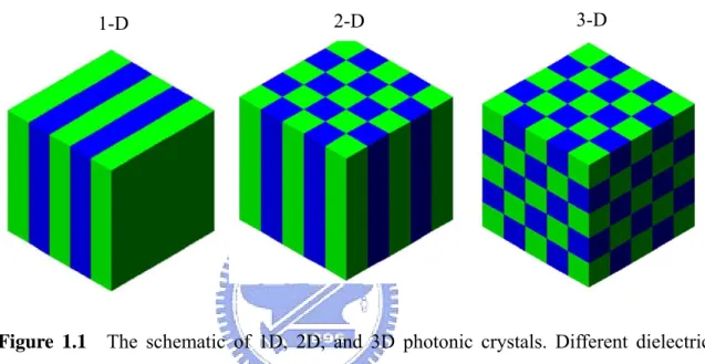
(13) three-dimensional (3D) according to the periodicity arrangements of dielectric materials along one or more axes. The Fig. 1.1 is illustrated these three classification of photonic crystals. Owing to the difficulty in fabrication process, most applications in photonic crystals are focused on 1D and 2D photonic crystals. And 3D photonic crystals are emphasized the investigation on fabrication process.. 2-D. 1-D. Figure 1.1. 3-D. The schematic of 1D, 2D, and 3D photonic crystals. Different dielectric. constants are represented in the different colors. (Adopted form reference [2]). The most important characteristic of photonic crystals is photonic band gap. In order to investigate the photonic band gap, we can study from the electronic band theory. In the electronic band theory, the behavior of electron would be affected by periodic crystal structure and obey Schrodinger equation: ⎡ h ⎤ 2 ⎢⎣− 2m* ∇ + V (r )⎥⎦ψ (r ) = Eψ (r ). where m* is the effective mass of electron, V (r ) is the potential function of periodic crystal structure, and ψ (r ) is the electronic wave function. The square of ψ (r ) denotes the existence probability of electrons in space, and E is eigen-value of electron energy. When the. ψ (r ) term is equal to zero in certain energy levels, it means that the existence probability of -2-.
(14) electron in these energy levels is zero. Then these energy levels construct the electronic band gap in electronic band structure.. The behavior of light in photonic crystals is analogous to electron in crystal. The periodic dielectric variations in photonic crystals act as the lattice of atoms in crystals. Deriving from the Maxwell’s equations, we get the master equation: 2. ⎛ 1 ⎞ ⎛ω ⎞ ∇ × ⎜⎜ ∇ × H (r ) ⎟⎟ = ⎜ ⎟ H (r ) ⎝ ε (r ) ⎠ ⎝c⎠ where ε (r ) is the function of dielectric constant variation. For a given ε (r ) we can solve the master equation and get the corresponding H (r ) . Then the corresponding eigen-values and eigen-vectors can be obtained and a photonic band structure can be shown by calculation. When the H (r ) term becomes exponential decay in certain frequency, it means that light is forbidden propagating in these frequencies. And the forbidden zone is called the photonic band gap. A photonic crystals band structure of the 2-D triangular lattice photonic crystals with r/a=0.3 and a=500nm is shown in Fig, 1.2. And the x-axis and y-axis in Fig. 1.2 indicate the wave vector and normalized frequency. The band structure is calculated by 2-D plane wave expansion (PWE) method. The shadow region between the first band (named dielectric band) and the second band (named air band) formed the photonic band gap.. -3-.
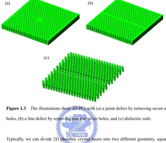
(15) Figure 1.2. A typical TE mode 2-D photonic crystals band structure calculated by 2-D. plane-wave expansion (PWE) method. The shadow region is the PBG of this 2-D photonic crystals with r/a = 0.3 and a = 500 nm.. Furthermore, when we want to take advantage of the PBG effect, we can construct artificial defects by removing parts of the periodic structure in photonic crystals to manipulate photons inside the defects. In general, we construct the defects in two different types. One is formed by removing one or more air holes and called point defects as shown in Fig. 1.3 (a). This kind of defects has been used to construct the photonic crystal micro-cavities. The other one is formed by removing one or more row of air holes and called line defects as shown in Fig. 1.3 (b). This kind of defect has been used in low-loss photonic crystal waveguide. The light in specific frequency localized or propagated in these defects will get ultra-low loss because of the PBG effect. Constructing point and line defects in photonic crystals will give rise to localized modes within the band gaps and hence allow us to confine and manipulate the flow of light in these structures. Excluding air holes type in 2D photonic crystals, we can also construct the 2D photonic crystals by using periodic arrangement of dielectric rods as shown in Fig. 1.3 (c).. -4-.
(16) (a). (b). (c). Figure 1.3 The illustrations show 2D PCs with (a) a point defect by removing seven air holes, (b) a line defect by removing one row of air holes, and (c) dielectric rods.. Typically, we can divide 2D photonic crystal lasers into two different geometry, square lattice [3, 4] and triangular lattice [5, 6]. 2D photonic crystals with a triangular lattice have become most popular structure due to its large photonic band gap effect. A micro-cavity laser with a wide range of tailored modes excitable by the active layer within the cavity can be created by removing several selected air-holes lattice, or modifying the parameters of the inner holes near cavity region [7, 8]. 2D photonic crystal lasers were first demonstrated by O. Painter et al. in 1999. As shown in Fig. 1.4, the photonic crystal patterns are defined on the 2D dielectric material slab. And a micro-cavity is formed by several missing air holes in photonic crystal patterns. The undercut is fabricated in order to form a symmetric cavity structure. In this structure, the vertical confinement is provided by a symmetric waveguide structure and the photonic crystal pattern provides the in-plane confinement by its well-known photonic crystal band-gap. -5-.
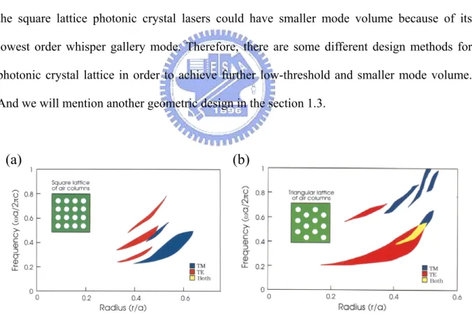
(17) Figure 1.4 The scheme of 2D photonic crystal micro-cavity. (Adopted from reference [7]). In the same r/a ratio, a photonic crystal laser with triangular lattice is much easier demonstrated than square lattice owing to the broader PBG as shown in Fig. 1.5. However, the square lattice photonic crystal lasers could have smaller mode volume because of its lowest order whisper gallery mode. Therefore, there are some different design methods for photonic crystal lattice in order to achieve further low-threshold and smaller mode volume. And we will mention another geometric design in the section 1.3.. (a). Figure 1.5. (b). Gap map for (a) square and (b) triangular lattice of air columns with dielectric. medium, ε = 11.4 . PBG of a triangular lattice is usually broader than that of square lattice, in the same r/a ratio. The yellow region in (b) is called a complete band gap which included the photonic band gaps with TM mode and TE mode. (Adopted form reference [2]) -6-.
(18) 1.2. Microdisk Laser. The microdisk lasers have a high quality (Q) factor due to the strong optical confinement by the total internal reflection at the interface between semiconductor and air. The microgear laser is a kind of microdisk laser with rotationally symmetric grating, which matches with the profile of the whispering gallery mode (WGM) [9]. The WGM is significantly discussed from the resonant modes in microdisk and microgear lasers. The WGM is optically confined in the form of standing wave around the microdisk edge by the total internal reflection effect caused by the index contrast between the air cladding and the microdisk. For the grating number of microgear is equal to the number of WGM standing wave, the different phase non-lasing mode is completely suppressed by the enhancement of the field mismatch. In opposite, for the inphase lasing mode, the lasing phenomenon is obtained by the strongly confined single mode. (a). Figure 1.6. (b). Scheme of a microgear laser and resonant modes. (a) Microgear laser with H z. standing wave of WGM matched with the grating number. (b) H z. 2. of resonant modes.. (Adopted from reference [9]). When the cavity size of microgear is reduced to close to the diffraction limit of the WGM, the Q factor is seriously degraded. A fusion with quasi-periodic photonic crystals and microgear lasers was demonstrated by T. Baba et al. in 2003 [9]. Using the fusion with -7-.
(19) quasi-periodic photonic crystals solves the minimization of cavity size problem in microgear laser. Because of the geometry of quasi-periodic photonic crystals is approximate to the microgear lasers, we can also find high Q factor WGMs which sustained by 1D TIR and 2D PBG effect.. 1.3. Quasi-Periodic Photonic Crystal Laser. So far, we propose that the anisotropy of a photonic band gap is dependent on the periodicity of the photonic crystal lattice. Their essential feature is the formation of Bloch states as a result of the periodic perturbation from the lattice with translational symmetry. In 1998, however, Chan et al. calculated the density of state in a quasi-period photonic crystal instead of in the periodic one. They also found the complete photonic band gaps as well as triangular lattice photonic crystal [10].. Quasi-periodic photonic crystals have neither true periodicity in real space nor translational symmetry. As we called, it has a quasi-periodicity that exhibits long-range order and rotational symmetry. In general, a photonic crystals is represented the rotational symmetry order less than such as triangular and square lattice. Any other order of rotational symmetry, 8-, 10-, 12-fold, etc. is possible in quasi-periodic photonic crystals as shown in Fig. 1.7. Recently, quasi-periodic photonic crystals are studied because of the larger degrees of freedom for modifying optical properties than in photonic crystals [11, 12].. -8-.
(20) (a) Figure 1.7. (b). (c). The scheme of (a) octagonal, (b) decagonal, and (c) dodecagonal quasi-periodic. photonic crystal lattice. (Adopted from reference [13, 14]). Complete band gaps have been found in photonic crystals. The anisotropy of photonic band gap is dependent on the symmetry of the photonic crystal lattice. As the order of symmetry increases, the Brillouin zone becomes more circular, resulting in an isotropic band gap. In triangular lattice, the symmetry level is six. Higher symmetry level can be achieved by the more complex geometries, the concept of quasi-crystal in solid-state is applied. In order to achieve higher order of symmetry, certainly, the more complex geometries of quasi-periodic photonic crystals are designed, as shown in Fig. 1.7. As the mirror of micro-cavity, more isotropic and efficient PBG confinement can be provided by QPC, which leads to lower threshold. Up to date, only few experimental efforts dealing with localized states in the quasi-periodic photonic crystals structure have been reported, for example, T. Baba. et al. have recently reported a whispering gallery mode (WGM) laser based on a quasi-periodic photonic crystals. So do the Y. H. Lee et al., they report the localized modes in a dodecagonal quasi-periodic photonic crystals single cavity laser. They also modify the inner-most holes which are concentrated strongly on the dielectric region on the purpose to achieve high -9-.
(21) quality factor.. High quality factor WGM can be sustained in quasi-periodic photonic crystal micro-cavity with proper modification. In order to obtain the well-confined WGM, the constructive interference condition has to be satisfied at the cavity boundary and the standing wave should be formed in the nearest air holes of a microgear like cavity. The well-confined WGM profile in magnetic field with azimuthal number six of the modified micro-cavity should be obtained. And the number of lobes would match with the number of gears formed by the nearest air hole.. 1.4. An Overview of This Thesis. In this thesis, we investigate the basic characteristics of Dodecagonal (12 fold) QPC (DQPC) D2 (formed by 7 missing air-holes) micro-cavity with whispering gallery mode (WGM). The following chapters are included the basic theory of our design, simulation results, setup and procedures of fabrication, photoluminescence (PL) measurement results and analysis. The device structures and simulation results are introduced in the chapter 2. Fabrication procedures of membrane structure are demonstrated in chapter 3. In chapter 4, the lasing characteristics of DQPC D2 and PC D2 micro-cavities with two different lattice variation regions are measured by NIR micro-PL system. Besides, the measurement results were further compared and analyzed. Then, the basic lasing characteristic and coupling behaviors in DQPC twin and triple-cavity are also shown in chapter4. A brief conclusion of my research is presented in the last chapter.. - 10 -.
(22) Chapter 2. Simulation of Quasi-Periodic Photonic Crystal. 2.1.. Introduction. In chapter1, we introduce the basic theory of photonic crystal. In this chapter, we will illustrate the devices structure and the numerical methods which are used to calculate the characteristic of photonic crystal. We can verify our design and measurement results by using these numerical methods. The band diagrams of periodic symmetry photonic crystal were calculated by plane-wave expansion (PWE) method. And the resonance modes in micro-cavity were calculated by finite-different time-domain (FDTD) method. In the latter of this chapter, we will demonstrate the simulation results in our research.. 2.2.. Finite-Difference Time-Domain Method. To solve the differential form of Maxwell’s equations, we can replace the differential form with differencing form, and expand the differencing form to obtain the basic FDTD equation. Because the time-domain technique can cover a wide frequency range with single simulation run, FDTD method is the one of the most popular method to simulate the electromagnetic wave in the photonic crystal.. As simulating by FDTD method, Maxwell’s curl equations are given in the following: uv uv ∂ B uuv ∇×E = − − Jm ∂t uv uuv ∂ D uuv ∇×H = + Je (2.1) ∂t uuv uuv J J e where and m denote electric current source and magnetic current source. Then, we - 11 -.
(23) substitute the relation of them into (2). We can obtain:. uv uuv σ uv ∂E 1 = ∇× H − E ε ∂t ε uuv uv ρ ' uuv 1 ∂H = − ∇× E − H µ µ ∂t. (2.2). where ε is the electrical permittivity, µ is the magnetic permeability, σ is the electrical conductivity, and ρ ' is an equivalent magnetic resistivity. The magnetic resistivity term is. uuv uv J ∇ ⋅ B = 0 , m provided to yield symmetric curl equations. By the Maxwell’s diverge equation is absent. Therefore, the magnetic resistivity term is absent. Because of small variation of magnetic permeability in materials, we assume that the magnetic permeability in materials is equal to that in free space. And the material is assumed to be lossless, which implies that σ is equal to zero. In a rectangular coordinate system, equation (2.2) is equal to the following system of scalar equations:. ∂H x 1 ∂E y ∂Ez = − ( ) ∂t µ0 ∂z ∂y ∂H y. (2.3). 1 ∂Ez ∂Ex ( ) − µ0 ∂x ∂z. (2.4). ∂H z 1 ∂Ex ∂E y ( ) = − ∂t µ0 ∂y ∂x. (2.5). ∂t. =. ∂Ex 1 ∂H z ∂H y ) = ( − ∂t ∂z ε ∂y ∂E y 1 ∂H x ∂H z ) = ( − ∂t ∂x ε ∂z ∂Ez 1 ∂H y ∂H x = ( − ) ∂t ∂y ε ∂x. (2.6) (2.7) (2.8). The six partial differential equations are the basic of the FDTD equations. For numerical calculation, we shall transform differential equations above into differencing equations. We denote a space point in a rectangular lattice as : - 12 -.
(24) (i, j, k ) = (i∆x, j∆y, k ∆z). (2.9). and for any function of space and time we put :. F n (i, j , k ) = F (i∆x, j∆y, k ∆z, n∆t ). (2.10). where ∆x , ∆y , and ∆z are the lattice space increments in x, y, z coordinate direction, ∆t is the time increment, and i, j , k , and n are integers. By using the centered finite-difference approximation for the spacial and temporal differential equations, we can obtain :. ∂F n (i, j , k ) F n (i + 12 , j , k ) − F n (i − 12 , j , k ) = ∂x ∆x n n 1 ∂F (i, j , k ) F (i, j + 2 , k ) − F n (i, j − 12 , k ) = ∂y ∆y ∂F n (i, j , k ) F n (i, j , k + 12 ) − F n (i − 12 , j , k − 12 ) = ∂z ∆x ∂F n (i, j , k ) F = ∂t. n + 12. (i, j , k ) − F ∆t. n + 12. (i, j , k ). (2.11). uv uuv To substitute equation (2.11) into equation (2.3 – 2.8), Yee put the components of E and H uv uuv at an unit cell of rectangular lattice And Yee evaluated E and H at alternate half time step as shown in Fig. 2.1.. H. E. H. E t. (n-1/2)Δt. (n)Δt. (n+1/2)Δt. (n+1)Δt. uv uuv E and H components. Figure 2.1 Temporal division of. Then, we substitute equation (2.11) into equation (2.5) and equation (2.8) to obtain - 13 -.
(25) uv uuv E and H components in the z-direction, we have:. n+ 1. Hz. 2. n− 1. (i + 12 , j + 12 , k ) = H z. 2. (i + 12 , j + 12 , k ) +. ∆t. µ0. ⋅{. 1 [ Exn (i + 12 , j + 1, k ) − Exn (i + 12 , j , k )] ∆y. 1 [ E yn (i + 1, j + 12 , k ) − E yn (i, j + 12 , k )]} (2.12) ∆x ∆t 1 n+ 1 n+ 1 1 1 2 2 ⋅ { [ H ( i + , j , k + ) − H (i − 12 , j , k + 12 )] Ezn +1 (i, j , k ) = Ezn (i, j , k + 12 ) + y 2 2 ε (i, j , k + 12 ) ∆x y −. −. 1 n+ 1 n+ 1 [ H x 2 (i, j + 12 , k + 12 ) − H x 2 (i, j − 12 , k + 12 )]} ∆y. (2.13). The equations corresponding to equation (2.3), (2.4), (2.6), (2.7) can be similarly. uv uuv E and H constructed. By the system of finite-difference equations, the new value of the component at any lattice point depends only on its previous value and on the previous values. uv uuv E and H component at adjacent points. of the. As the electromagnetic wave propagates in homogeneous dielectric, the propagating velocity in the x, y, z direction is the same. But the propagating velocity in the diagonal direction is faster than that in the x, y, z direction. Therefore, the simulating wave will cause distortion as the propagating time increase. In order to reduce the space error between the x, y, z direction and the diagonal direction, the space grid size must be chosen such that an increment of the electromagnetic field does not change significantly. And the time grid size is also chosen for the stability. For constant ε and µ , computational stability implies :. ∆t ≤. 1 1 1 1 c ( )2 + ( )2 + ( )2 ∆x ∆y ∆z. This requirement puts a restriction on ∆t for our chosen ∆x , ∆y , and ∆z . - 14 -. (2.14).
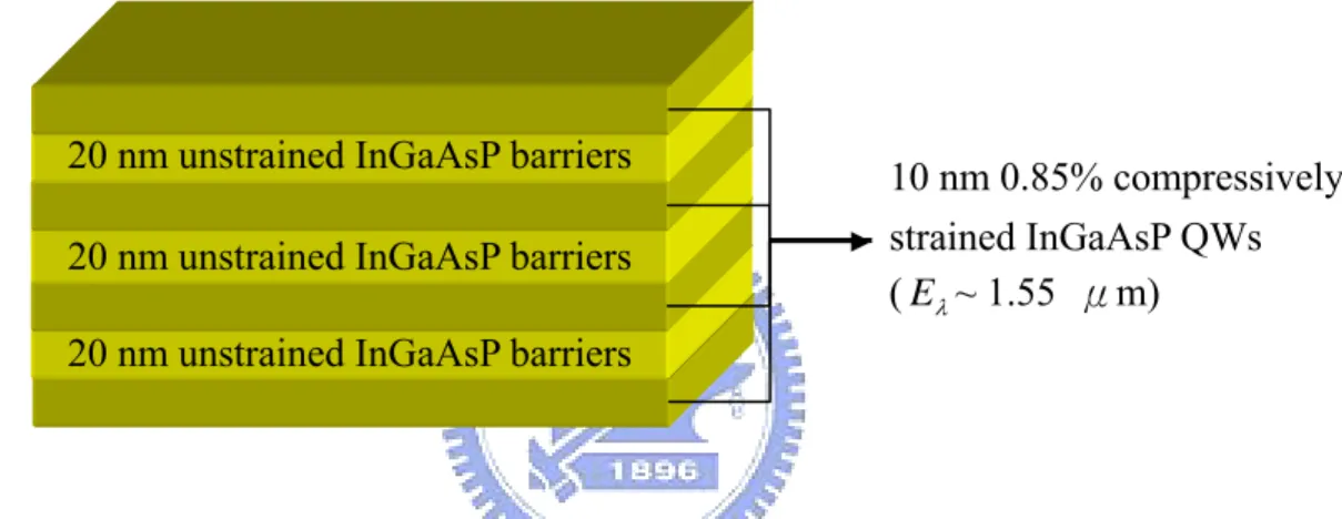
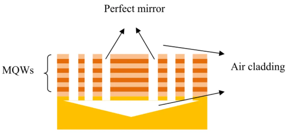
(26) 2.3.. Devices Structures. In our research, we have a common goal to fabricate our devices at communication wavelength. As shown in Fig. 2.2, the epitaxial structure consists of four 10 nm 0.85% compressively strained InGaAsP quantum wells (QWs) which are separated by 20 nm unstrained InGaAsP barriers. Then, the active epitaxial layer of our devices had a PL spectral bandwidth from 1480 to 1580 nm and centered at 1550nm as shown in Figure. 2.3.. 20 nm unstrained InGaAsP barriers. 10 nm 0.85% compressively strained InGaAsP QWs ( Eλ ~ 1.55 μm). 20 nm unstrained InGaAsP barriers 20 nm unstrained InGaAsP barriers. Figure 2.2. The illustration of our designed epitaxial structure. In a symmetric structure, we fabricated the QWs slab to be a thin dielectric membrane surrounded by upper and lower air cladding. Membrane structure is one of the most popular structures in related researches, such as J. D. O’Brien, T. Baba, S. Noda. et al. have reported their important achievement by using membrane structure .. In Fig. 2.3, we illustrate the mechanism of strong optical confinement for both in-plane and vertical directions in a 2-D photonic crystal slab structure. The PBG effect is used for optical confinement as perfect mirrors in the in-plane direction, and total internal reflection (TIR) effect at the interface between the slab and the air cladding in the vertical direction. Because of the strong optical confinement in this membrane structure micro-cavity, high - 15 -.
(27) quality factor (Q) and ultra-small mode volumes can be achieved. The fabrication procedures in detail will be introduced in chapter 3.. Perfect mirror. Air cladding. MQWs. Figure 2.3. The scheme of the membrane structure. The light will be confined in. membrane structure by perfect mirrors in the in-plane direction and the TIR effects of the air cladding in the vertical direction.. - 16 -.
(28) 2.4.. Simulation Results. 2.4.1. WGM Mode Dependence. In recent years, various photonic crystal (PC) cavities with different lattice designs are considered, such as square, triangular, quasi-periodic lattice, and so on. Although PC micro-cavities are widely investigated both in theory and experiments, up to date, only a few groups make efforts on the study of localized states in quasi-periodic photonic crystal (QPC) laser structure, which include Baba et al. and Y. H. Lee et al.. In the pervious research of our group, we investigate the basic lasing characteristic in the DQPC D2 micro-cavity. And we calculate the frequencies and profiles of resonance modes using 2D or 3D FDTD method. One calculated resonance mode of DQPC D2 micro-cavity presents zero-order radial WGM profile with azimuthal number six (W6 mode) as shown in Fig. 2.4. W6 mode is a very potential mode due to its high quality factor contributed to the good consistency with cavity geometry and relative small mode volume compared to the cavity. More important, its central node with zero field distribution is quite suitable for electrical injection structure used in micro-disk lasers.. Figure 2.4 The illustration of WGM in DQPC D2 micro-cavity - 17 -.
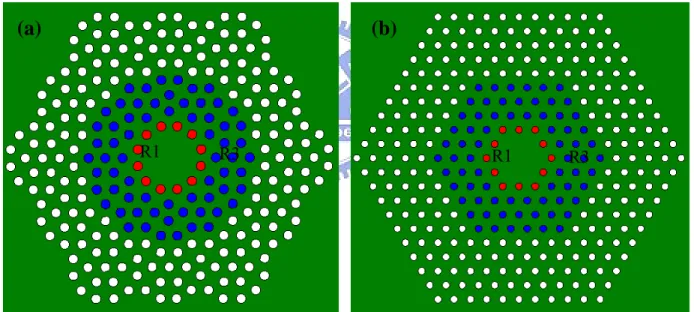
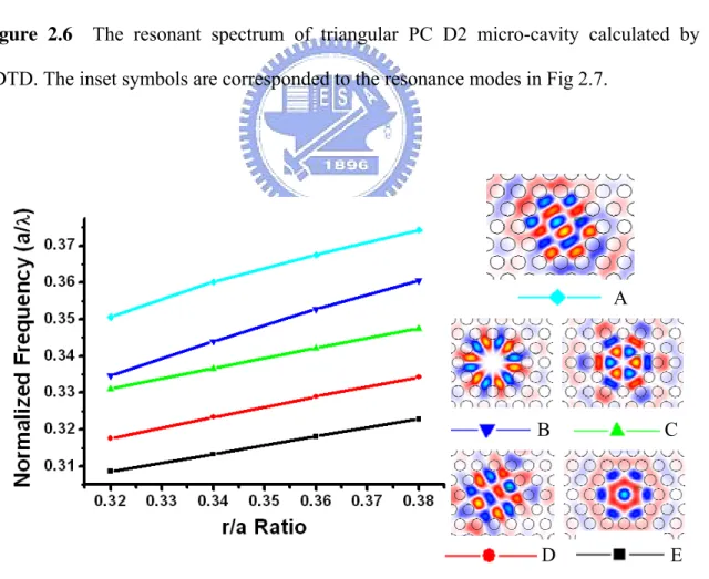
(29) In this thesis, moreover, we want to investigate the fabrication tolerance and WGM mode dependence of DQPC D2 micro-cavity. Hence, in order to investigate its fabrication tolerance, we fabricate DQPC D2 micro-cavities with two different lattice variation regions, which are the inner-most air-hole region (named R1) and the outer air-hole region (named R3) as shown in Fig. 2.5 (a). The variation degree is 0% to 7%. For comparison, we also fabricate traditional triangular PC D2 micro-cavity with the same lattice variation regions as shown in Fig. 2.5 (b). It should be noticed that the lasing mode of triangular PC D2 micro-cavity is not the WGM. By them under the same condition with each other, we can demonstrate the WGM mode dependence in DQPC further. And the measurement result will show in the chapter 4.. (a). (b). R1. R3. R1. R3. Figure 2.5 The schemes show the lattice-varied inner-most layer (R1) and the outer. layer (R3) air-holes in (a) DQPC D2 micro-cavity (b) triangular PC D2 micro-cavity. In order to analyze the resonance modes in triangular PC D2 micro-cavity, we performed the 2D FDTD analysis with the approximated effective index 2.7. A triangular PC D2 micro-cavity is simulated with lattice constant of 540 nm and the r/a ratio of 0.32. The calculated resonant spectrum is shown in Fig. 2.6. In the Fig. 2.7, it shows the normalized - 18 -.
(30) frequency a/λ of lasing modes with the various r/a ratio. The right inset shows the corresponding mode profiles.. D. E. B C A. Figure 2.6. The resonant spectrum of triangular PC D2 micro-cavity calculated by 2D. FDTD. The inset symbols are corresponded to the resonance modes in Fig 2.7.. A. Figure 2.7. B. C. D. E. The plot of the normalized frequencies of resonance modes versus the different. r/a ratio. The corresponding mode profiles are shown on the right insets. - 19 -.
(31) 2.4.2. Quasi-Periodic Photonic Crystal Twin and Triple-Cavity. Photonic molecule is an optical analog to the chemical molecule, whose behavior is similar with electronic energy state in hydrogen molecule. According to the strong WGM mode dependence on inner-most air holes of DQPC D2 micro-cavity, we assume that the WGM will also sustain in DQPC D2 twin-cavity. Based on WGM in DQPC micro-cavity, we design a new-type DQPC coupled twin-cavity. The similar structure in microdisk has been demonstrated by Baba et al. in 2005 [15, 16]. They demonstrate the bistable lasing in a photonic molecule consisting of twin microdisk [17]. Due to the diffraction limit of the WGMs, however, there is the minimization of cavity size problem in microdisk laser. When the cavity size of microdisk is reduced to close to the diffraction limit of the WGM, the Q factor is seriously degraded. Moreover, the device often exhibits a non-lasing mode very close to the lasing mode. This mode is thought to have a phase-shifted mode profile against the lasing mode profile. In addition to the disadvantages mentioned above, the coupling behavior is very sensitivity to the disk spacing due to the decaying evanescent field. In order to solve these problems, we want to realize the twin-cavity device in DQPC lattice. First, in DQPC lattice structure, the size of fabricated device can be less than the diffraction limit. We can fabricate the device smaller than microdisk. Second, because of the micro-gear effect in DQPC micro-cavity, un-wanted resonance mode in DQPC coupled twin-cavity will be greatly reduced, especially for π-phase-shifting modes and high order WGM. In addition, there will be no un-necessary degeneracy states due to the restriction of micro-gears formed by the nearest air holes. Finally, by using DQPC lattice with PBG and larger field penetration depth, the coupling behavior is much easier to control. Hence, we fabricate the twin-cavity device in DQPC lattice and measure the basic lasing characteristics. This design will be the key unit of new optical-buffer devices and bi-stable switches with logic operation based on photonic crystal coupling-resonator optical-waveguide (CROW). - 20 -.
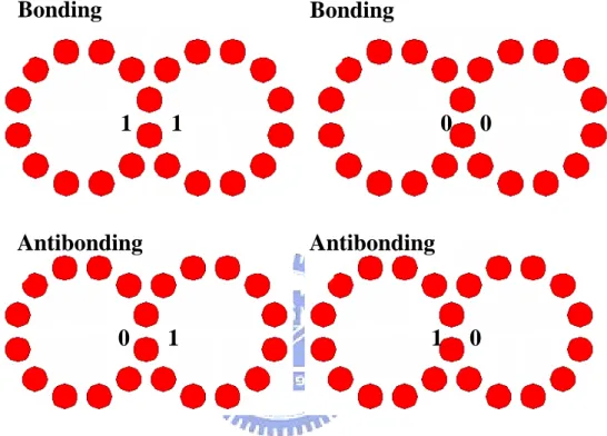
(32) At first, the lasing mode could be classified into bonding and antibonding mode according to the parities of coupled states. In Figure 2.9, it denotes the bonding and antibonding mode respectively. The number one means the high state in field distribution. Oppositely, the number zero means the low state.. Bonding. Bonding. 1. 1. Antibonding. 0. 0. 0. Antibonding. 1. 1. 0. Figure 2.8 The parities of coupled states in DQPC D2 twin-cavity. Afterward we calculate the profiles of resonance modes by using 3D FDTD method in order to verify our supposition. In Fig. 2.9, it shows the CAD layout in 3D simulation software. The green region means the membrane slab, which thickness is 220 nm. And the effective index is 3.4. A calculated result of resonance mode spectrum is shown in Fig. 2.10. The normalized frequency a/λ of resonance modes versus the r/a ratio and the corresponding mode profile are shown in Fig. 2.10. From the simulation results, we can confirm the previous supposition. And we do not find other phase-shifting and degeneracy states of bonding and antibonding modes in our simulation. This indicates the well-controlled coupled behavior in DQPC twin-cavity. - 21 -.
(33) Figure 2.9. The 3D CAD Layout of DQPC D2 twin-cavity. Antibonding. Bonding. Figure 2.10 The illustration shows the normalized frequency of calculated resonance modes. with the different r/a ratio. The corresponded mode profiles are shown on the right inset.. Based on DQPC twin-cavity unit, we can also calculate different multi-coupled micro-cavity geometry. We expand the DQPC D2 micro-cavity into triple-cavity. According to the parities of coupled states, the resonance modes can be classify into BBB and AAB mode, which mean three bonding nodes and two antibonding nodes plus one bonding node, respectively as shown in Fig.2.11. The calculated result of triple-cavity indicates only two - 22 -.
(34) coupling mode parity, which is very different from those in micro-disks and much easier to analyze. In microdisk, the coupling mode parity will equal to the number of the micro-cavity and include lots of degeneracy states. Hence, we believe the DQPC triple-cavity will be a good candidate for bi-stable switch applications with multi-ports.. BBB. BBB. 1 1. 1. 1. 1. 0 1. 0 0. 0. AAB. 0. 0. 0. 0. AAB. 0 1. 0. 1. 0. 0. 1. 1 1. 1. Figure 2.11 The parities of coupled states in DQPC D2 triple-cavity. And then we use the 3D FDTD simulation to verify the coupling mode parity in DQPC D2 triple-cavity. The 3D CAD layout of DQPC D2 triple-cavity is shown in Fig. 2.12. And the plot of calculated normalized frequency of resonance modes versus the different r/a ratio is shown in Fig. 2.13. The corresponding mode profiles are in the right insets. - 23 -.
(35) Figure 2.12. The 3D CAD Layout of DQPC D2 triple-cavity. AAB. BBB Figure 2.13. The illustration shows the normalized frequency of calculated resonance modes. with the different r/a ratio. The corresponding mode profiles are shown on the right insets.. - 24 -.
(36) 2.5.. Conclusion. In this chapter, the basic theory of FDTD method is introduced as first. And then the device structure of our membrane structure is presented. The resonance modes of triangular PC D2 micro-cavity are calculated by 2D FDTD method. In the end, we introduce the parities of coupled states in DQPC D2 twin and triple-cavity. The resonance modes of DQPC D2 twin-cavity and triple-cavity are calculated by 3D FDTD method. From the simulation results, we can confirm the bonding and antibonding mode in DQPC D2 twin-cavity. In DQPC D2 triple-cavity we also obtain the supposed resonance modes of AAB and BBB mode.. - 25 -.
(37) Chapter 3. Fabrication of Membrane Structure Photonic Crystal Laser. 3.1.. Introduction. The structure design and simulated results of quasi-periodic photonic crystals have been introduced in chapter 2. In this chapter, the fabrication processes of membrane structure quasi-periodic photonic crystals lasers will be presented and discussed. And then the real devices will be fabricated.. 3.2.. Fabrication of Two-Dimensional Photonic Crystal Laser. 3.2.1. Epitaxial Structure. The epitaxial structure of InGaAsP with strained/unstrained MQWs structure has been introduced in previous chapter. A complete structure for membrane fabrication is shown in Fig. 3.1. The epitaxial structure consists of four 10 nm 0.85% compressively strained InGaAsP quantum well layers which are separated by three 20 nm unstrained InGaAsP barrier layers. The epitaxial structure of MQWs is served as the active layers of the membrane structure devices. It has been confirmed that the photoluminescence (PL) spectrum of the MQWs is centered at 1550 nm with 200 nm span as shown in Fig.3.2. The MQWs layers are grown on InP substrate by metalorganic chemical vapor deposition (MOCVD) and then a 60 nm InP cap layer is deposited on it for protecting the MQWs during a series of dry etching processes.. - 26 -.
(38) 60 nm InP cap layer 57.5 nm InGaAsP 20 nm unstrained InGaAsP barriers 20 nm unstrained InGaAsP barriers. 10 nm 0.85% compressively strained InGaAsP QWs ( Eλ ~ 1.55 μm). 20 nm unstrained InGaAsP barriers 57.5 nm InGaAsP InP Substrate. Figure 3.1. The scheme of epitaxial structure of InGaAsP QWs for membrane QPC. lasers. The thickness of active region is about 220 nm.. Figure 3.2. A typical PL spectrum of our MQWs. The gain peak is centered at 1550. nm with 200nm span.. - 27 -.
(39) 3.2.2. Dielectric Deposition. Before the deposition procedure, a series of surface cleaning is necessary. First, we dip the wafer into BOE solution for few seconds in order to remove the negative oxide from InP. Then we put the wafers into acetone solution and use the ultra-sonic vibrator to clean the particles on the surface. Owing to a series deposition and etching processes later, the above surface cleaning is very important.. After the surface cleaning, we deposited a Si3N4 layer with 140 nm on the wafer as an etching hard mask by SAMCO PD-220 plasma enhanced chemical vapor deposition (PECVD). The thickness of Si3N4 is decided by the selective dry etching ratio in ICP/RIE pattern transfer process. In fabrication of membrane structure, a Si3N4 hard mask with thickness of 140 nm is good enough for dry etching to achieve the etched depth about 800 nm into InP/InGaAsP layer. The SiH4/NH3/N2 mixture gases are used to deposit dielectric hard mask on 300℃ substrate at 35W plasma power in 100Pa pressure.. 3.2.3. Photonic Crystal Patterns Definition. The photonic crystal patterns are defined by JEOL JSM-6500F electron-beam lithography (EBL) system. The EBL system is a field-emission scanning electron microscope which employs a schmasky type fields-emission gun as the electron source. The EBL system has been adjusted with Nanometer Pattern Generation System (NPGS). It provides a user-friendly environment for the delineation of complex structures using a commercial electron microscope. It can easily write patterns on wafer by CAD tools. The resolution of EBL system is about 1.5 nm for 15KV scanning electron microscope (SEM) and 20 nm for lithography. Accelerating voltage of electron-beam is increased from 0 KV to 30 KV. And the - 28 -.
(40) electron resister will be developed above 100 µA electron-beam.. At first, we put the sample into acetone solution and use the ultra-sonic vibrator to clean the particles on the surface. Second, an A5 polymethylmethacrylate (PMMA) resist layer is spin-coated on the sample by spin coater with two spinning steps, 1000 rpm for 10 seconds and 3500 rpm for 25 seconds, respectively. And then the sample is put on a 180℃ hotplate for 90 seconds in order to do the soft-baking process. In this recipe, the thickness of PMMA layer is estimated as 300 nm. If a smaller radius of air hole is needed, a thinner thickness of PMMA is better for development. The A3 PMMA can be spin-coated about 100 nm thickness on the sample. After the soft-baking process, the uniformity of PMMA must be checked by naked eyes. The uniformity is determined by gloss from the sample.. Choosing a proper dosage of electron-beam is an important issue in EBL. Generally, there are two methods to test the dosage of electron-beam. In the first method, we can cut a sample into two parts. One of the samples is used for testing dosage with wide range. After the fixing and developing process, we coat a thin Pt layer on the sample in order to increase the conductivity and prevent PMMA from electron-beam. And then we use the SEM system to choose the proper dosage of electron-beam. Finally, the other sample is used to write the PC patterns in the best dosage which we test from the former one.. In the other method, we will not cut the sample and do testing and writing process in the same wafer. After the testing process in wide range and the development process, we can choose the proper electron dosage by optical microscope. And then we put the sample into acetone solution and use the ultra-sonic vibrator to remove the PMMA and defined patterns. Finally, we repeat the same steps to write again with the proper dosage in the same position. In this method, we must check that all conditions in the testing and writing process are the - 29 -.
(41) same, especially the uniformity of PMMA.. Certainly, determining the proper electron dosage from the wide range correctly is the key point to write good patterns on sample. In the SEM pictures, if there are still some residues of PMMA inside the air holes, the shape of holes are not good for photonic crystal. The residual PMMA resulted from the insufficient electron dosage on sample. Oppositely, if the electron dosage is sufficient, the shapes of air holes are closely to a circle. And there is no residue of PMMA inside the air holes.. Generally, the proper shape of air holes in QPCs are situated at a slightly overdose condition. Therefore, the radius in the designed CAD files must be 20 nm ~ 30 nm smaller than the expected pattern size. Furthermore, the proximity effect also has to be considered in CAD design. Because of this effect, the inner-most air holes are slightly smaller than others. This problem can be solved by lager radius design of inner-most air hole in CAD files.. Finally, in the development process, the sample is developed in MIBK solution at temperature between 24 to 25℃ for 70 seconds. If the temperature of development solution is over to 28℃, the PMMA layer will become deformed and the shape of the air holes will distort. After the development process, the sample was put into the IPA solution about 30 seconds for cleaning the residues.. 3.2.4. Patterns Transfer. After the patterns definition by EBL system, the patterns transfer processes are introduced as follows. In order to transfer the QPC patterns into InP layer, an Oxford Instruments Plasma Technology Plasmalab 100 inductively coupled plasma reactive ion - 30 -.
(42) etching (ICP/RIE) system is used. Before the hard mask etching, the sample is etched by O2 plasma in order to clean the residual PMMA in air holes. And then the Si3N4 hard mask is etched by CHF3/O2 mixed gases in RIE mode dry etching. The Si3N4 etching environment recipes are 150W RF power and 55 mTorr at 20℃. The gas flow rate of CHF3 and O2 are 5 sccm and 50 sccm, respectively. The etching rate in CHF3/O2 mixed gas is about 1.5 nm/s on average and the selectivity ratio to PMMA is 8.. After transferring the patterns to Si3N4 layer, we use the O2 plasma to remove the PMMA layer. If the patterns are good enough, we could continue doing the next process, or we can repeat from Si3N4 depositing process in the same sample. Afterward, the InP / InGaAsP MQWs layer is etched by H2/CH4/Cl2 mixed gases in ICP mode dry etching. The MQWs etching environment recipes are 73W RF power, 1000W ICP power and 4 mTorr at 150℃. The gas flow pressure of H2, CH4, and Cl2 are 0.8, 0.4 and 0.3 mTorr, respectively. The etching rate in H2/CH4/Cl2 mixed gas is 5.5 nm/s on average and the selectivity ratio to Si3N4 is 6.. 3.2.5. Substrate Undercut. In order to fabricate the membrane structure, the InP substrate below the MQWs should be removed. The undercut can be constructed by using a mixture solution with HCl : H2O = 4 : 1 at 0℃ for 9 minutes. This process also removes the 60 nm InP cap layer and smoothes the surface and the sidewall of the air holes. This process could be also regarded as a gentle wet etching process to reduce the optical loss caused by the surface roughness. Although wet etching process is anisotropic, the InP wet etching stops at 95° and 40° from <-1, 0, 0> direction in the (0, -1, -1) plane and the (0, 1, -1) plane. It results from the material characteristic of InP. Generally, we can define the opening windows at front and end of the - 31 -.
(43) photonic crystal patterns alone the (0, 1, -1) orientation of the InP substrate to break the etching stop planes and form the undercut. As shown in Fig. 3.3 (a), the dark regions indicate the opening windows. In Fig. 3.3 (b), the SEM picture shows the fabricated device including the windows. The central underline indicates the V-shaped undercut.. Windows regions. Windows regions. Figure 3.3. (a) The designed CAD file of 2-D triangular lattice PC micro-cavity. The. dark regions indicate the windows for undercut process. (b) The SEM picture of fabricated device.. In the former patterns definition process, if the PC patterns do not parallel to the (0, 1, -1) direction of InP material exactly, the undercut line would be distorted. Hence, in order to ensure the PC pattern parallel to the (0, 1, -1) direction, we can use the parallel line in EBL system to aim at (0, 1, -1) direction of the sample before electron-beam writing process. In Fig. 3.3 (b), we can see the undercut line of real device is parallel to the devices. Besides, modifying the mechanism in wet etching process can also improve the undercut process. We put a magnetic rotator in the wet etching solution in order to keep the etching solution being refreshed at the surface of sample. Thus, we will get better performance in the undercut process. - 32 -.
(44) 3.3.. Fabrication Results. The fabrication procedures of the membrane structure PC lasers are introduced in previous section. In this section, all of the demonstrated devices in my research will be shown by the SEM pictures.. 3.3.1. Photonic Crystal with Random Lattice Variation. To verify mode dependence on 12-nearest air-holes and its fabrication tolerance of DQPC D2 micro-cavity, we fabricate the traditional 2D triangular PC D2 micro-cavity with random lattice variation in the inner-most air hole region and the outer air hole region. And the variation degree is 0% to 7%. We fabricate the real device in array. In this array, the lattice constant increases from 530 nm to 560 nm with the increment 10 nm and the r/a ratio increases from 0.32 to 0.38. In Fig. 3.4, the SEM pictures show the top and side-view of real devices with membrane structure. The line in V-shape trench can be observed from the side view of the membrane structure as show in Fig. 3.4 (c).. (a). (b). - 33 -.
(45) (c). (d). Figure 3.4. The SEM pictures of 2D triangular PC D2 micro-cavity lasers array. (a). Top view. (b) The zoom-in picture of (a). (c) Side view. (d) The illustration of suspended membrane structure.. 3.3.2. Dodecagonal Quasi-Periodic Photonic Crystal Twin and triple-cavity. Following the previous research of WGM in single cavity, we extend the WGM mode into DQPC twin and triple-cavity. And we investigate the coupling behavior in these novel structures. In Fig. 3.5 and Fig. 3.6, the SEM pictures show the top and side-view of DQPC twin and triple-cavity.. (a). Figure 3.5. (b). The SEM pictures of DQPC D2 twin-cavity laser. (a) Top view. (b) Side view. - 34 -.
(46) (a). (b). Figure 3.6. The SEM pictures of DQPC D2 triple-cavity laser. (a) Top view. (b) Side. view.. 3.4.. Conclusion. Fig. 3.7 shows an overview of fabrication processes of 2D photonic crystal micro-cavity membrane lasers. Here is a summary of introduced fabrications in this chapter. The epitaxial structure consisting of four 10 nm compressively-strained InGaAsP MQWs as the active layer with 1550 nm central wavelength is prepared. And then, a 140 nm silicon-nitride layer served as hard mask for latter etching process is deposited on the epitaxial wafer by PECVD system. And the PMMA layer is spin-coated on the Si3N4 layer. The PC or QPC patterns are defined on the PMMA layer by EBL and transferred to the Si3N4 layer by RIE process with CHF3/O2 mixed gases. Then the patterns are further transferred to MQWs by ICP dry etching with CH4/Cl2/H2 mixed gases at 150℃. Finally, the membrane structure is formed by selective wet etching with the mixture of HCl and H2O at 0℃.. - 35 -.
(47) InP Substrate. MQWs. Si3N4. PMMA. Fabrication Procedure. Epitaxial Structure. Dielectric Deposition. PMMA Coating. Patterns Definition. Patterns Transfer. PMMA Remove. Patterns Transfer. Dielectric Remove. Substrate Undercut. Figure 3.7. An overview of fabrication processes of 2D photonic crystal membrane. structure lasers.. - 36 -.
(48) Chapter 4. 4.1.. Measurement Results. Measurement Setup. In order to measure the lasing characteristics of our fabricated devices, including 2D triangular photonic crystal micro-cavity with random lattice variation and dodecagonal quasi-periodic photonic crystal with multi-cavities, we use a micro-photoluminescence (micro-PL) system with sub-micrometer scale resolution in space and sub-nanometer scale resolution in spectrum. The simple configuration of the micro-PL system is shown in Fig 4.1.. Optical Spectrum Analyzer Collective Lens White Light Source. Function Generator. IR Camera. 50/50 Beam splitter. 845 nm TTL Laser. Pumping Source Emission Light. 100X Objective Lens. Optical Fiber. Sample. Figure 4.1. The configuration of micro-PL system. - 37 -. Monitor.
(49) In the micro-PL system, an 845 nm laser diode is used as the pump source. This TTL laser diode can be operated with pulse mode and continuous-wave (CW) mode by switching a function generator. In our measurement, we use the pulse mode with pulse-width 25 ns and 0.5% duty cycle at room temperature. The pump beam is reflected into a 100x long working distance NIR objective lens which is mounted on a 3-axis stage with numerical aperture of 0.5 by a 50/50 beam splitter. The 48% reflection in angle 45° of the splitter for 845 nm wavelength is confirmed. And the pump beam is focused to a spot about 1.5 µm in diameter by the objective lens.. The objective lens collects the emitted light from the top of the sample. We use a collective lens to focus the output signal into the slit of our optical spectrum analyzer, with 0.05 nm resolution. An InGaAs detector with good responsibility from 900 nm to 1600 nm is used to obtain the lasing spectra of our devices. All of the following measurement results are measured by this micro-PL system.. 4.2.. WGM Mode Dependence. To investigate WGM mode dependence on 12-nearest air-holes and its fabrication tolerance, we randomly vary the lattice positions of DQPC D2 micro-cavity and triangular PC D2 micro-cavity in two different regions. The illustration of the inner-most air-hole-layer region (R1) and the three outer-air-hole-layer region (R3) in DQPC D2 micro-cavity laser is shown in Fig. 2.6. The variation degree is 0% to 7%. The lasing spectra with the two different lattice variation regions R1 and R3 under the same pumping conditions are shown in Figure 4.2.. - 38 -.
(50) (a) R3 R1. (b). Figure 4.2. The lasing spectra of varied (a) R1 and (b) R3 region. The wavelength. variations of them are ± 10 and ± 2 nm.. Comparing the lasing spectra in Fig. 4.2, we can observe WGM mode dependence on 12-nearest air-holes of DQPC D2 micro-cavity. In Fig. 4.2 (a), the shift of lasing peak wavelength is about ± 10 nm in the random variation in R1 region. In contrast, the shift of lasing peak wavelength is only about ± 2 nm in R3 region which is much smaller than that in R1 region. Consequently, the shift of lasing wavelength is dominated by the inner-most air holes in DQPC D2 micro-cavity. And we can conclude that the W6 WGM mode has strong dependence on the inner-most air-holes. On the other hand, the lattice variation of 2nd, 3rd and 4th layer in DQPC D2 micro-cavity laser will not affect the shift of lasing wavelength significantly. - 39 -.
(51) Table 4.1 shows the percentage of lasing devices with different random lattice variation region. The sampling device is over 300. According to the statistic result of Table 4.1, we could confirm the fabrication tolerance is up to 4% lattice constant shifting in R1 region and 7% in R3 region. Therefore, the lasing mode of 12-fold QPC laser is sensitivity to the position of inner-most air-holes. And we can clearly indicate the mode dependence again.. Table 4.1. The percentage of lasing devices under different random lattice variation. degrees measured from over 300 samples.. Variation. R1. R3. 4%. 100 %. 100 %. 5%. 70 %. 100 %. 7%. 45 %. 90 %. We also measured the thresholds of these two cases with different variation degrees. The measurement results are shown in Table 4.2. The thresholds of R3 case are almost the same and that of R1 case show a fast degradation when the variation degree is larger than 3%. These also indicate the large fabrication tolerance and strong mode dependence mentioned above, again.. - 40 -.
(52) Table 4.2 The thresholds of devices with different random lattice variation degrees for. DQPC D2 lasers.. Variation. R1. R3. 0%. 0.25 mW. 0.25 mW. 3%. 0.57 mW. 0.24 mW. 4%. 0.91 mW. 0.24 mW. 5%. 0.4 mW. 0.23 mW. 7%. No lasing. 0.24 mw. We also calculate the mode profiles of the micro-cavity with two different random variation regions under the same variation degree 5% by using 2D FDTD method. By comparing the two simulation results shown in Fig. 4.3 (a) and (b), we can observe that the W6 WGM mode in DQPC D2 micro-cavity is quite sensitive to the positions of the inner-most air-holes.. Figure 4.3. (a) The WGM mode profile of DQPC D2 micro-cavity with 5% variation of R1.. (b) The WGM mode profile of DQPC D2 micro-cavity with 5% variation of R3. - 41 -.
(53) For comparison, we also fabricate traditional triangular PC D2 micro-cavity with two different lattice variation regions. First, in order to identify the lasing mode of triangular PC D2 micro-cavity is not WGM, we compare the measurement results to the 2D FDTD simulation results as shown in Fig. 4.4. The typical lasing spectrum of the lasing mode is shown in Fig. 4.5. The lasing wavelength is 1515.8 nm. The inset of Fig. 4.5 shows the near-threshold lasing spectrum. The measured full-width at half-maximum (FWHM) is 0.3 nm and the side mode suppression ratio (SMSR) is about 20 dB as shown in Fig. 4.6.. Measurement data. Figure 4.4 The illustration shows the normalized frequency of calculated lasing modes with. the different r/a ratio. The black circles denote the measured data. The corresponding lasing mode profiles are shown in the right inset.. - 42 -.
(54) 1515.82 nm. Figure 4.5. 0.3 nm. A typical lasing spectrum above threshold of the triangular PC D2 micro-cavity. laser. The inset indicates near-threshold lasing spectrum.. 20 dB. Figure 4.6. A lasing spectrum above threshold of the triangular PC D2 micro-cavity laser in. dB scale. The SMSR is about 20 dB.. After measuring the basic lasing characteristic of the triangular PC D2 micro-cavity without any lattice variation, we measure the shift of lasing peak wavelength in R1 region and R3 region. The lasing spectra with the two different lattice variation regions under the same pumping conditions are shown in Fig. 4.6. In Fig. 4.7, the random variation in R1 region, the - 43 -.
(55) shift of lasing peak wavelength is about ± 5 nm. In R3 region, the shift of lasing peak wavelength is about ± 3 nm. In DQPC D2 micro-cavity, the ratio of peak wavelength shift in R1 and R3 region is 5. On the other hand, in PC D2 micro-cavity, the ratio of peak wavelength shift in R1 and R3 region is only less than 2. Comparing with the measurement results between DQPC D2 micro-cavity and PC D2 micro-cavity, we can verify the WGM mode dependence on the inner-most air-holes of DQPC D2 micro-cavity again. However, in most PC micro-cavity, for example, triangular PC D2 micro-cavity, WGM is weakly confined and exists with only several hundreds or lower Q factor due to the mismatch between cavity boundary and its mode profile. This mode dependence implies that one can enhance or well localize a high Q WGM in different PC micro-cavity by modifying only the inner-most air-hole of the micro-cavity to be a circular geometry.. - 44 -.
數據
+7
相關文件
To complete the “plumbing” of associating our vertex data with variables in our shader programs, you need to tell WebGL where in our buffer object to find the vertex data, and
(Another example of close harmony is the four-bar unaccompanied vocal introduction to “Paperback Writer”, a somewhat later Beatles song.) Overall, Lennon’s and McCartney’s
Read and test MBR in the order of bootable devices configured in BIOS.. Load bootstrap
It is useful to augment the description of devices and services with annotations that are not captured in the UPnP Template Language. To a lesser extent, there is value in
Using regional variation in wages to measure the effects of the federal minimum wage, Industrial and Labor Relations Review,
Plane Wave Method and compact 2D Finite difference Time Domain (Compact 2D FDTD) to analyze the photonic crystal fibe.. In this paper, we present PWM to model PBG PCF, the
The fist type of photonic crystal fiber is composed of a solid silica core with modulation core refractive index and a cladding with triangular lattice elliptical air holes,
The advantages of using photonic crystal fibers (PCFs) as gas sensors include large overlap and long optical path interaction between the gas and light mode field and only a
