國立交通大學
電子物理研究所
博士論文
披覆銻砷化鎵之砷化銦量子點的能帶結構工程及元件應用
Band Structure Engineering and Device Applications of
GaAsSb-Capped InAs Quantum Dots
研究生:廖昱安
指導教授:綦振瀛 博士
張文豪 博士
披覆銻砷化鎵之砷化銦量子點的能帶結構工程及元件應用
Band Structure Engineering and Device Applications of
GaAsSb-Capped InAs Quantum Dots
研究生:廖昱安 Student:Yu-An Liao
指導教授:綦振瀛 博士 Advisors:Dr. Jen-Inn Chyi
張文豪 博士 Dr. Wen-Hao Chang
國立交通大學
電子物理研究所
博士論文
A Thesis
Submitted to Institute of Electrophysics College of Science
National Chiao Tung University in partial Fulfillment of the Requirements
for the Degree of Doctor of Philosophy
in Electrophysics September 2013
Hsinchu, Taiwan, Republic of China
i
披覆銻砷化鎵之砷化銦量子點的能帶結構工程及元件應用
研究生: 廖昱安 指導教授: 綦振瀛 博士 張文豪 博士 國立交通大學 電子物理研究所博士班 摘要 本論文旨在探討披覆銻砷化鎵之砷化銦量子點的能帶結構調變工程及其元件應用, 主要內容包含兩個主題。在論文的第一個部分,我們利用四種方法去調變披覆銻砷化鎵 之砷化銦量子點的能帶結構。首先,我們改變銻砷化鎵披覆層中銻的組成,並由時間解 析光譜技術研究載子的動態行為,無論由變功率光激螢光光譜峰值的位移或由較長的時 間衰減常數,都證實了在異質接面所形成的第二型能帶結構;不同的載子復合路徑也藉 由變溫量測得以區分。第二種方法為熱退火處理。除了明顯的螢光峰值藍位移及光譜線 寛縮減外,熱退火所引起的合金混合也造成輻射復合速率的增加及消除在銻砷化鎵披覆 層的載子侷限態。同時,在變功率及時間解析螢光的量測中,我們也觀察到由第二型變 成第一型的能帶結構變化。第三種方法為披覆層厚度的調變。我們發現發射光的能量和 載子復合生命期都與披覆層厚度有密切的關係。理論計算也指出量子侷限和電洞波函數 分佈對披覆層厚度的變化相當敏感。同時,銻原子造成的量子點尺寸變化在其光學特性 上也扮演相當重要的角色。最後我們採用了銻砷化鋁鎵四元化合物披覆層。由變功率及 時間解析螢光量測的結果,披覆銻砷化鎵之砷化銦量子點的第二型能帶結構能藉由加入 鋁元素而轉變為第一型能帶結構,而這個能帶結構的轉變也同時從理論計算得到證實。 披覆銻砷化鎵之砷化銦量子點的元件應用為本論文第二部分的重點。首先,我們探 討披覆砷化鎵層之砷化銦紅外線量子點光檢測器的光譜響應。相較於傳統的砷化銦紅外 線量子點光檢測器,其呈現較窄的光譜線寛和較長的檢測波長,這些變化可歸因於銻砷 化鎵披覆層造成之尺寸較大且較均勻的量子點。同時,我們也藉由光激螢光激發光譜得 知其光譜響應的躍遷機制來源。另外一個應用為記憶體元件。為了簡化製程手續,我們 採用了寛通道平面式柵極電晶體的技術來研究披覆銻砷化鎵之砷化銦量子點的記憶體 效應。因此在探討記憶體元件前,我們先介紹俱砷化鎵片電阻之平面式柵極電晶體。在 有效控制片電阻的摻雜濃度情況下,理想的電流調變特性和高集極電流之間可取得平衡。 其調變開關特性的機制,是藉由操控表面自由電子分佈來空乏元件通道。此外,光電流 的量測結果也顯示出該技術有應用於光檢測器的潛力。在對寛通道平面式柵極電晶體了 解後,我們展示室溫下使用寛通道平面式柵極電晶體之砷化銦量子點充放電的能力。相 較於第一型量子點,俱銻砷化鎵披覆層之第二型量子點呈現出較長的充放電時間。由披 覆銻砷化鎵之砷化銦量子點提供之較慢的電荷弛豫和簡化的平面式柵極電晶體技術,揭 示該元件俱有實際應用的潛力。ii
Band Structure Engineering and Device Applications of
GaAsSb-Capped InAs Quantum Dots
Student: Yu-An Liao Advisors: Dr. Jen-Inn Chyi Dr. Wen-Hao Chang
Institute of Electrophysics National Chiao Tung University
ABSTRACT
This dissertation is devoted to band structure engineering and device applications of GaAsSb-capped InAs Quantum Dots (QDs). In the first part of this dissertation, four approaches are utilized to tailor the band alignments of GaAsSb-capped InAs QDs. First, carrier dynamics of GaAsSb-capped InAs QDs with different Sb composition were investigated by time-resolved photoluminescence (TRPL). Both the power dependence of PL peak shift and the long decay time constants confirm the type-II band alignment at the heterointerface. Different recombination paths have been clarified by temperature dependent measurements. Second, we study the effects of thermal annealing on the emission properties of type-II GaAsSb-capped InAs QDs. Apart from large blueshifts and a pronounced narrowing of the QD emission peak, the annealing induced alloy intermixing also leads to enhanced radiative recombination rates and reduced localized states in the GaAsSb capping layer (CL). Evidences of the evolution from type-II to type-I band alignments are obtained from time-resolved and power-dependent PL measurements. The third approach is the modulation of the CL thickness. Both the emission energy and the recombination lifetime are found to be correlated with the CL thicknesses. Theoretical calculations indicate that the quantum confinement and the wave function distribution of hole states are sensitive to the GaAsSb CL thickness. The Sb induced change in QD size also plays a role in the optical properties of GaAsSb-capped QDs. The last approach is using the quaternary AlGaAsSb CL. As evidenced from power-dependent and time-resolved PL measurements, the GaAsSb-capped QDs with type-II band alignment can be changed to type-I by adding Al into the GaAsSb CL. The evolution of band alignment with the Al content in the AlGaAsSb CL has also been confirmed by theoretical calculations. The PL thermal stability and the room temperature PL efficiency are also improved by AlGaAsSb capping.
Device applications of GaAsSb-capped InAs QDs are demonstrated in the second part of this dissertation. First, spectral responses of GaAsSb-capped InAs/GaAs quantum-dot infrared photodetectors (QDIPs) with different Sb composition are investigated. Compared with the conventional InAs/GaAs QDIPs with wide detection windows, a much narrower
iii
spectral width is observed for GaAsSb-capped QDIPs at longer detection wavelengths. The phenomenon is attributed to the larger InAs QDs with improved uniformity resulted from the GaAsSb CL. In this case, lowered energy states and reduced energy difference in-between would result in longer detection wavelengths with narrower spectral widths of GaAsSb-capped QDIPs. By comparing with photoluminescence excitation spectra of the samples, the dominant transition mechanisms for GaAsSb-capped QDIPs are also investigated. The other application is memory device. To further simplify the fabrication procedure, the architecture of wide-channel in-plane gate transistors (IPGTs) is adopted to demonstrate the memory effect of GaAsSb-capped InAs QDs. Hence, we studied IPGTs with an n-GaAs sheet resistance prior to the investigation of memory device. A trade-off between effective current modulation and high saturation drain current is obtained by optimizing the doping density of the sheet resistance. The mechanism responsible for the transistor behaviors of the devices is due to the channel electron depletion related to the population of mobile surface electrons under different gate biases. The photocurrent measurements demonstrate that the IPGT architecture is a feasible approach for the applications of photodetectors. After having the idea of the wide-channel IPGT, we demonstrate room-temperature electron charging/discharging phenomena of InAs QDs using wide-channel IPGTs. The device based on type-II GaAsSb-capped InAs QDs exhibits both the longer charging and discharging times than those of the type-I counterpart with GaAs CL. The slow charge relaxation of GaAsSb-capped InAs QDs and simple architecture of IPGT reveal the potential of this device architecture for practical memory applications.
iv
CONTENTS
Chinese Abstract i English Abstract ii Contents iv List of Figures viChapter 1 General Introduction 1
1.1. Overview of Self-Assembled Quantum Dots 1 1.2. Impacts of the GaAsSb Capping Layer on the Underlying
Self-Assembled InAs Quantum Dots 6 1.3. Outline of this Dissertation 9
Chapter 2 Band Structure Engineering in GaAsSb-Capped InAs Quantum Dots 11 2.1. Varying the Antimony Composition 11 2.1.1 Experimental details 11 2.1.2 Optical properties 12 2.1.3 Temperature-dependent measurements 16 2.2. Rapid Thermal Annealing 20 2.2.1 Experimental details 20 2.2.2 Effects of thermal annealing on the emission properties 21 2.2.3 The evolution of band alignments 27 2.3. Modulation of Capping Layer Thickness 29 2.3.1 Experimental details 29 2.3.2 Effects of GaAsSb capping layer thickness on the optical properties 30 2.3.3 Simulations 34 2.4. Quaternary AlGaAsSb Capping Layer 38 2.4.1 Experimental details 39 2.4.2 The evolution of band alignments 40 2.4.3 Simulations 43
v
Chapter 3 Device Applications of GaAsSb-Capped InAs Quantum Dots 47
3.1. Quantum-Dot Infrared Photodetectors 47 3.1.1 Sample structures and device fabrications 48 3.1.2 Spectral responses and the corresponding transition mechanisms 49 3.2. Wide-Channel In-Plane Gate Transistors 56 3.2.1 Experimental details and device fabrications 57 3.2.2 Operation mechanisms 58 3.2.3 Photodetector applications 61 3.3. Memory Devices 64 3.3.1 Sample structures and experimental setups 65 3.3.2 Migration speed of surface mobile electrons 66 3.3.3 Carrier charging/discharging behaviors 68
Chapter 4 Conclusions 74
References 77
vi
LIST OF FIGURES
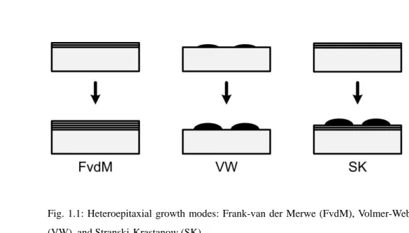
Fig. 1.1: Heteroepitaxial growth modes: Frank-van der Merwe (FvdM),
Volmer-Weber (VW), and Stranski-Krastanow (SK). ... 3 Fig. 1.2: Schematic band diagrams of InAs QDs with GaAs1-xSbx CLs. ... 7
Fig. 2.1: PL spectra of the GaAs1-xSbx capped InAs QDs with different x. ... 12
Fig. 2.2: (a) Power dependent PL spectra of the 16% sample. (b) The GS and the ES peak energies as a function of Pex1/3 for the 16% sample. ... 13
Fig. 2.3: TRPL decay traces for the GaAs1-xSbx capped InAs QDs with different x. ... 14
Fig. 2.4: (a) The schematic illustration of a time-dependent recombination rate of non-equilibrium carriers. (b) The sample structure and the underlying recombination processes responsible for the faster (1) and the slower (2) decay components. ... 15 Fig. 2.5: Temperature evolution of the PL spectra (a) and decay traces (b) for the
x=16% sample. ... 16
Fig. 2.6: (a) The PL peak energy as a function T. Lines are fitting curves with (solid) and without (dashed) localization effects. (b) An Arrhenius plot of the time-integrated intensities for the faster (I1) and the slower (I2) decay
components. ... 18 Fig. 2.7: PL spectra (a) and TRPL decay traces (b) for the as-grown and annealed
InAs/GaAsSb QDs, together with the reference InAs/GaAs QDs. ... 21 Fig. 2.8: Energy dependent carrier lifetimes and time evolution of the PL spectra for
the samples annealed at (a) 700 °C and at (b) 800 °C. ... 23 Fig. 2.9: The schematic illustration of hole redistribution among fluctuant potentials
and the corresponding energy dependent lifetime. ... 25 Fig. 2.10: Radiative recombination rate as a function of the annealing temperature.
vii
Fig. 2.11: Power dependent PL spectra for the samples annealed at (a) 900 °C, (b) 800 °C, and (c) 700 °C. (d) The peak energy of QD ground state as a function of Pex1/3. ... 28
Fig. 2.12: The PL spectra measured at T= 12 K for the investigated QD samples with different CL thickness t. ... 30 Fig. 2.13: The cross-sectional TEM images for the samples with different CL
thicknesses. ... 31 Fig. 2.14: Power-dependent PL spectra for the GaAsSb-capped samples with a CL
thickness of (a) 2.5 nm, (b) 5 nm, (c) 10 nm. All the PL spectra have been offset and the intensities have been normalized to their ground-state peak. (d) The ground-state peak energy of the QDs as a function of Pex1/3. ... 32
Fig. 2.15: (a) TRPL spectra and (b) the deduced decay time for the investigated QD samples with different CL thickness t. ... 33 Fig. 2.16: The calculated wave functions of the hole ground state of the InAs QD
with a GaAsSb CL thickness of (a) 0 nm, (b) 2.5 nm, (c) 5 nm, and (d) 10 nm. (e) The electron-hole wave function overlaps and (f) the ground state transition energy as a function of the CL thickness, where the solid symbols are experimental data, while the solid curves (open symbols) are calculated results obtained from the first (second ) set of calculations. ... 35 Fig. 2.17: The RT PL spectra for the samples with a CL thickness of t = 0 and 2.5 nm.
... 36 Fig. 2.18: (a) The contour map of the unstrained VBO between AlxGa1-xAs1-ySby and
InAs as functions of the Al(x) and the Sb(y) contents. (b) A schematic of band alignments for AlGaAsSb-capped InAs/GaAs QDs. ... 38 Fig. 2.19: The PL spectra measured at T = 12 K for the GaAs-capped and
AlGaAsSb-capped InAs QDs with different Al contents (x). ... 40 Fig. 2.20: (a) The ground state PL peak energies as a function of Pex1/3. (b) TRPL
spectra for the investigated samples. (c) The ground state PL peak energies as a function of Al contents (x). (d) The estimated wave function overlaps according to the measured decay lifetimes. ... 41 Fig. 2.21: (a)-(d) The calculated wave function distributions for the hole ground state
on the (1-10) plane for different Al contents (x=0, 0.1, 0.2, 0.3) in the CL. (e)-(h) The calculated band structures along the growth direction through
viii
the center of the QD (solid line, A) and through the CL near the QD base (dotted line, B). (i) The ground state PL peak energies as a function of Al contents and (j) the estimated wave function overlaps according to the measured decay lifetimes, where the curves are the calculated transition energy and wave function overlaps as function of Al content... 44 Fig. 2.22: (a) Arrhenius plot of the integrated PL intensity for GaAs-capped and
AlGaAsSb-capped InAs QDs with x = 0.3. (b) The PL spectra measured at RT. ... 45 Fig. 3.1: (a) The 10 K PL spectra and (b) PL peaks as a function of cube roots of
excitation powers P1/3 for GaAsSb-capped samples with different Sb content x. ... 49 Fig. 3.2: Normalized 10 K spectral responses of GaAsSb-capped devices with
different Sb content x at 1.2 V. ... 51 Fig. 3.3: 10 K PLE spectra of x=0 and 20 % sample and 10 K spectral responses of
x=0 and 20 % device. The x-axis of the PLE spectra is re-adjusted by
setting the QD first excited state as the “zero” energy. The insets depict the schematic conduction band structures and corresponding transitions response for the spectral responses. ... 52 Fig. 3.4: The normalized responsivity ratios of x=0 and 20 % device at 1.2 V under
different incident light polarizations. ... 54 Fig. 3.5: (a) RT ID–VGS curves of devices with different n-GaAs doping density n.
(b) RT ID–VDS curves of the device with n= 5×1017 cm−3 at VGS= 5, 0, and
−5 V. ... 58 Fig. 3.6: Top-view picture and the schematic cross-sectional diagram of the IPGTs. ... 60 Fig. 3.7: (a) Normalized photocurrents of the device with n-GaAs channeldoped to
5×1017 cm−3 and another device with 20-nm In0.1Ga0.9As channel n-type
doped to 1×1018 cm−3 operated at VDS=1 V and VGS=0 V at RT. (b) RT
spectral response curves of the device with 20-nm In0.1Ga0.9As channel
n-type doped to 1×1018 cm−3 operated at VDS = 1 V and different gate
biases. ... 62 Fig. 3.8: The wafer structures of the investigated QD memory samples. ... 65 Fig. 3.9: The RT (a) ID-VGS curve and (b) time-resolved drain currents (VGS jumps
ix
Fig. 3.10: The RT ID-VGS curves of GaAs-capped and GaAsSb-capped QD devices
measured at VDS=1 V under different sweeping directions of the gate bias. ... 68
Fig. 3.11: The RT time-resolved drain currents of GaAs-capped and GaAsSb-capped QD devices measured at VDS=1 V. The gate bias VGS changes from 5 to -5
V at t=0.5 s. ... 70 Fig. 3.12: The schematic band diagrams of GaAs-capped QD device (a) before and
(b) after the bias switching. The counterparts of GaAsSb-capped are shown in (c) and (d), respectively. The notations EF,G and EF,S represent the Fermi
levels near the gate terminal and substrate side, respectively. ... 71 Fig. 3.13: The RT time-resolved drain currents of GaAs-capped and GaAsSb-capped
QD devices measured at VDS=1 V. The gate bias VGS changes from -15 to 5
1
Chapter 1 General Introduction
1.1. OVERVIEW OF SELF-ASSEMBLED QUANTUM DOTS
Low-dimensional phenomena have been urgent and inevitable challenges toward the next generation semiconductor devices in the recent decades. Scaling down the dimensional of semiconductor structures not only saves space and increases the capacity of a single chip, but also brings the benefits of quantum effects. When the size of the material is reduced to the nanometer scale in one direction, the freedom of electron movement is lost in that direction. This confinement results in the quantization of the electron energy and in the variations of the electron density of states, which is the most remarkable and significant benefit of low-dimensional semiconductor technology. It has been considered that these quantization effects in a semiconductor structure can make an electronic device more efficient. For instance, Quantum wells, where electrons are confined in a plane, have been extensively utilized in our daily life. If material dimension are further reduced to restrict electrons in a small volume, quantum dots (QD) are formed. QDs are tiny semiconductor nanoparticles, which range from nanometers to tens of nanometers in size. With carrier confinement in three dimensions, the density-of-states of QDs are discrete, or so-called ä-function-like. The unique strongly size-dependent optical and electrical properties are differential to those of the corresponding bulk material. Furthermore, QDs are expected to have great potentials and advantages in several varieties of applications in optoelectronics.
Generally, semiconductor QDs can be manufactured by two main approaches. The first one is utilizing the lithography to pattern and etch the quantum well semiconductor structures.
2
The way is like to “carve out” QDs from bulk semiconductor materials. Although this conventional technique is convenient for mass-production of QDs, it is difficult to form QDs which are defect-free and exhibiting abrupt carrier confining potential. In addition, their high surface recombination rates due to the high surface-to-volume ratio, together with the damages introduced during the fabrication processes, significantly restrict them from optoelectronic applications. On the other hand, the other one is by mean of “growing” QDs from ad-atoms. It is the so-called self-assembled QDs [1,2] via heteroepitaxial growth in lattice-mismatched semiconductor system, such as typical In(Ga)As/GaAs and Ge/Si QDs which can be grown by using molecular beam epitaxy (MBE) or metal-organic chemical vapor deposition (MOCVD).
The formation of self-assembled QDs is by means of the self-assembled effects which are very common in strained semiconductor heterostructures. After Stranski and Krastanow first proposed the possibility of island formation on an initially flat heteroepitaxial surface in 1937, the growth of island formation on an initially two-dimensional (2D) layer by relaxing strain energy via misfit dislocations was generally referred to the Stranski-Krastanow growth mode (SK mode) [3]. In general, heteroepitaxial growth can be divided into three well-known modes depended on the interfacial surface energy and lattice mismatch [4]. They are Frank-van der Merwe (FvdM mode) [5], Volmer-Weber (VW mode) [6], and Stranski-Krastanow (SK mode) [3], which are schematically depicted in Fig. 1.1. For FvdM mode, it occurs in lattice-matched material systems and is commonly referred to as layer-by-layer growth mode. The deposited material wets the substrate when the surface energy of deposited material is lower than that of the substrate. On the contrary, when the surface energy of deposited material is larger, direct formation of three-dimensional (3D) islands will take place to minimize the system total energy, leading to the VW mode. The SK mode takes place in a lattice-mismatched system with small surface energy. Layer-by-layer growth is expected at the initial stage of growths. With the increasing amount of deposited
3
Fig. 1.1: Heteroepitaxial growth modes: Frank-van der Merwe (FvdM), Volmer-Weber (VW), and Stranski-Krastanow (SK).
material, the accumulated strain energy is getting larger. To release the strain energy, a transformation from the initially 2D growth to a 3D island growth occurs and the initial 2D layer underneath the islands is named “wetting layer”.
As far as the mechanism of strain relaxation, it was believed to occur not only through the formation of islands, but accompany the formation of misfit dislocations underneath. Some literatures have demonstrated the formation of coherently 3D strained islands without defect generations on InGaAs/GaAs system [7] and on Si/Ge system [4]. Since the elastic-deformation mechanism contributes to the lattice of the substrate approach to the strained island, the total strain energy can thus be lowered without introducing misfit dislocations. If the amount of deposited material were further increased, deformation of the substrate lattice will become unstable, leading to a transition of coherent SK islands back to the dislocated SK islands.
Relevant works are devoted to the optimized growth conditions in In(Ga)As/GaAs system [8-11]. The formed strained In(Ga)As islands are self-assembled with superior uniform size and shape distributions. The typical island revealed a favorable size with a
4
lateral dimension of 15~25 nm and a height of 3~5 nm. After the wide-band gap GaAs overgrowth, the islands behave like a quantum dot, which confines both the electron and the hole three-dimensionally by its surrounding GaAs of wider band gap, thus exhibiting atomic-like properties.
Accomplishments in acquiring high-quality and defect-free QDs not only open the door to the fundamental low-dimensional studies, but also stimulate developments of their applications in optoelectronic devices. One of the valuable applications is quantum-dot lasers. Relevant works were devoted to the development of quantum-dot lasers since Arakawa and Sakaki predicted quantum-dot lasers should have superior characteristics, such as ultra-low threshold, less temperature-dependence, and enhanced differential gain [12]. This is primarily because, as the dimension of materials is reduced, the density of state for electrons changes to give a narrower optical transition spectrum, making the light-matter interaction more efficient. The first demonstration of quantum-dot laser was reported by Kirstaedter et al. in 1994[13,14]. Improved operation by increasing the density of QDs was achieved by Bimberg
et al. in 1996 [15]. They also enabled high-power continuous-wave laser operations [16] by
stacking the QDs vertically which can achieve vertical coupling of the QDs [17].
Besides the applications in optical devices, self-assembled QDs have also been proposed for memory device applications. The read/write process in QD memory devices require low operation voltage since tunneling is employed for carrier injection and depletion [18]. With other advantages of high read/write speed, enhanced carrier storage capacity, and better endurance, QD memory devices are more reliable in comparison to other nonvolatile memory devices [19,20]. Lots of efforts have been devoted to the investigations of memory characteristics of InAs/GaAs QDs based on optically [21,22] and electrically [23-28] carrier injections. Room-temperature (RT) memory operations have also been demonstrated by using multi-stacked QD layers [22,23] and an optimized positioning of a single InAs QD layer in a local conduction band minimum [25].
5
More recently, a novel QD application of the intermediate-band solar cells (IBSC) has attracted much attention [29-31]. The concept is forming a mini-band in the active region of the solar cell. Thus, photons with sub-band gap energies can excite electrons to the continuum above the conduction band in a two-step process through the intermediate band, leading to a significant increase in the solar energy conversion efficiency. The QDs are ideal candidate for the creation of the intermediate band by composing of the ground states in close-stacked QDs. Within this framework, a limiting efficiency of 63.2% has been predicted for the IBSC, compared to 40.7% for conventional single gap solar cells [29]. The critical issue is their limited contribution to the total photocurrent due to the small volume of the QDs, so stacks of tens of QD layers are usually needed. However, it is well known to also increase the accumulated stress of the material during growth, generating dislocations and non-radiative recombination centers. Many efforts have dedicated to overcome the challenge, including introducing strain compensation layers [32,33].
Although varieties of applications of self-assembled QDs were successful demonstrated, these device are still far from the demands of commercial markets. The major problem is that QDs size uniformity is still not good enough. Besides, site-controlled QDs is an issue for other specific applications as well.
6
1.2. IMPACTS OF THE GAASSB CAPPING LAYER ON THE
UNDERLYING SELF-ASSEMBLED INAS QUANTUM DOTS
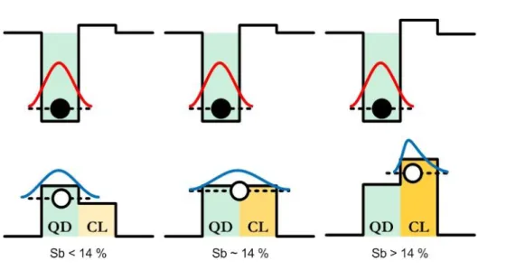
Self-assembled InAs QDs grown by MBE have been extensively investigated, relying on its mature development in the growth technique. However, the nature of self-assembled QD growth procedure makes it difficult to manipulate QD morphologies and the corresponding device performances such as detection wavelength tuning and inter-band emitting wavelength extending. To overcome this problem, one of the most straightforward solutions is the change of capping layer (CL) over InAs QDs from GaAs to different materials. In this case, similar QD morphologies can still be maintained while the band structures of InAs QDs with different CLs can be altered. Self-assembled InAs QDs with a GaAsSb CL have attracted much attention recently in the study of improving the performance of long-wavelength QD-based devices [34-37]. It has been reported that the impacts of the GaAsSb CL on the underlying InAs QDs are manifold. First, similar to the conventional InGaAs CL, the GaAsSb CL acts as a strain reducing layer for the QDs [38] and has great capability of tuning the emission wavelength towards 1.5 μm or beyond for telecommunication applications. Emission wavelength beyond 1.5 μm and RT continuous-wave operation of a 1.3 μm QD laser have been demonstrated. Second, the presence of Sb atoms in the CL is also helpful for suppressing the QD decomposition [39,40]. Typical GaAs-capped InAs QDs exhibit a truncated pyramid shape of about 4 nm due to strong Indium redistribution and/or out-diffusion during the capping processes, while that with the GaAsSb CL are lens-shaped with a height of about 8 nm. The enlargement in QD height improves carrier confinement and reduces the sensitivity of the excitonic band gap to QD size fluctuation within the ensemble. It has been shown that both effects can lead to a redshifted emission wavelength, an improved
7
Fig. 1.2: Schematic band diagrams of InAs QDs with GaAs1-xSbx CLs.
photoluminescence (PL) efficiency, and a narrower spectral width for Sb content less than 12-14%. The third and the most prominent effect is the large valence band (VB) offset at the InAs-GaAsSb heterointerface, which is beneficial to promote holes thermal stability. Schematic band diagrams of InAs QDs with the GaAs1-xSbx CL are shown in the Fig. 1.2.
When Sb content exceeds ~14 %, the heterostructure transforms from a type-I band alignment to a type-II band alignment [41,42].
Experimental evidences for the type-II QDs have been reported based on power-dependent PL and time-resolved PL (TRPL) measurements. Due to the spatial separation of electrons in the QDs and holes in the GaAsSb CL, the carrier lifetime should be much longer than their counterparts (i.e., InAs/GaAs QDs). Although such spatially indirect excitons with long carrier lifetimes [43,44] and the confinement of only one carrier species make the QDs very promising for memory [19] and photovoltaic devices [31,45], the degraded recombination efficiency is however detrimental for light emitting devices and laser applications. In addition, it has been pointed out that VB discontinuity plays an important role
8
in the design of multiple transition solar cells [46]. The use of antimony in the CL could have a strong advantage in obtaining a negligible VB offset, which is thought to be one of the key challenges in the development of QD-based solar cells. Hence, tailoring the transition energy, the band alignment, the wave function overlaps, and hence the carrier dynamics are desirable for specific applications. Several works have been devoted to achieve the goal, such as varying the Sb composition in the GaAsSb CL [40,41], post-growth thermal treatments [47,48], varying the GaAsSb CL thickness [49], graded Sb content in CL [50], or using quaternary GaAsNSb [51], InGaAsSb [52] and AlGaAsSb [53] CLs.
9
1.3. OUTLINE OF THIS DISSERTATION
The dissertation is devoted to optical properties and device applications of self-assembled InAs QDs with a GaAsSb CL. Before discussing the physics of the materials and the characteristics of the devices, an overview of self-assembled QDs and effects of the GaAsSb CL on the underlying self-assembled QDs are introduced in Chapter 1.
The keynote of Chapter 2 is the band alignment engineering of InAs QDs with a GaAsSb CL. We present four approaches to achieve the goal including varying the Sb composition in the CL, post-growth thermal treatments, thickness modulation of the CL, and quaternary AlGaAsSb CL. Varying the Sb composition in the CL, the most straightforward strategy, is discussed in Sec. 2.1. Carrier dynamics of InAs QDs with a GaAs1-xSbx CL were
investigated by TRPL. Besides confirming the type-II band alignment at the GaAsS-InAs interface from both the power dependence of PL peak shift and the longer decay time constants, different recombination paths have been clarified by temperature dependent measurements. Another alternative approach is the use of post-growth thermal annealing to smooth the VB discontinuity by the annealing induced alloy intermixing. In Sec. 2.2, we employed PL and TRPL spectroscopes to investigate the emission properties of the GaAsSb-capped InAs QDs after thermal annealing at temperatures ranging from 700 to 900
o
C. The annealing induced changes in the band alignment, the carrier dynamics and electronics structures due to the alloy intermixing were observed and discussed. In Sec. 2.3, we investigate the evolutions of emission energy and recombination lifetime of the GaAsSb-capped InAs QDs with the CL thickness. The effects of the CL thickness on the hole states and their wave function distributions are discussed and compared with theoretical calculations. For applications in long-wavelength light emitters, we demonstrate the tuning of band alignment and optical properties of InAs/GaAs QDs using a thin quaternary AlGaAsSb
10
CL in Sec. 2.4. As evidenced from power-dependent PL and TRPL measurements, the GaAsSb-capped QDs with type-II band alignment can be changed to type-I by adding Al into the GaAsSb CL. The evolution of band alignment with the Al content in the AlGaAsSb CL is also compared with theoretical calculations.
Following the idea of band alignment engineering and optical properties of GaAsSb-capped InAs QDs, the practical device applications are demonstrated in Chapter 3. Spectral responses of GaAsSb-capped InAs/GaAs quantum-dot infrared photodetectors (QDIPs) with different Sb composition are investigated in Sec. 3.1. By comparing with photoluminescence excitation (PLE) spectra of the samples, the dominant transition mechanisms for GaAsSb-capped QDIPs are also investigated. The narrow spectral width of the device is advantageous for selective detections at specific wavelengths for QDIPs. Another potential application of the type-II GaAsSb-capped InAs QDs is memory device. To further simplify the fabrication procedure, in-plane gate transistors (IPGTs) with micrometer-sized channel widths are adopted to demonstrate the memory effect of GaAsSb-capped InAs QDs. An IPGT with n-GaAs sheet resistance is investigated in Sec. 3.2. The photocurrent measurements demonstrate that the architecture is a feasible approach for the applications of photodetectors and the mechanism responsible for the transistor behaviors of the devices is also discussed. After having the ideas of IPGTs, we investigate room-temperature electron charging/discharging behaviors of InAs QD using IPGTs in Sec.3.3. The slow charge relaxation of GaAsSb-capped InAs QDs and simple architecture of IPGT reveal the potential of this device architecture for practical memory applications.
11
Chapter 2 Band Structure
Engineering in GaAsSb-Capped InAs
Quantum Dots
2.1. VARYING THE ANTIMONY COMPOSITION
The most straightforward strategy in tailoring the band alignment of InAs QDs with a GaAsSb CL is directly varying the Sb composition in the CL. It has been believed to exhibit a type-II band alignment when the Sb composition exceeds over 14%.Experimental evidences for the type-II transition have been reported based on power dependent PL measurements [41,42]. However, relevant reports regarding TRPL have been rare so far [43], which would provide a more direct evidence on the nature of radiative recombination in such type-II QDs.
In this section, we report a TRPL study on the GaAsSb covered InAs QDs. The much longer decay time confirms a type-II band lineup at the GaAsSb–InAs interface. Different recombination paths were discussed and identified by temperature dependent measurements.
2.1.1 Experimental details
The samples investigated in this section were grown on GaAs substrates by MBE. After the growth of a 200 nm thick GaAs buffer layer, a layer of InAs QD (2.7 ML, monolayer) was grown at 500 °C and subsequently capped by a 4.5 nm GaAs1−xSbx layer. Two samples
with nominal x of 16% and 21% were prepared. A sample with GaAs covered InAs QDs (x=0%) was also grown as a reference of type-I QDs. All samples were finally capped by a 50 nm GaAs layer. Atomic force microscopy of uncapped samples reveals that the QDs are lens
12
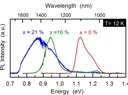
Fig. 2.1: PL spectra of the GaAs1-xSbx capped InAs QDs with different x.
shaped, with an average height of ≈8±0.5 nm, a diameter of ≈20 nm, and a density of 3×1010 cm−2. PL was excited by an argon ion laser (488 nm), analyzed by a 0.5 m monochromator and detected by an InGaAs photomultiplier tube. TRPL was performed using either a 200 fs Ti:sapphire laser (780 nm/80 MHz) or a 50 ps pulsed laser diode (405 nm/5 MHz). The decay traces were recorded using the time-correlated single photon counting technique with an overall time resolution of ~150 ps.
2.1.2 Optical properties
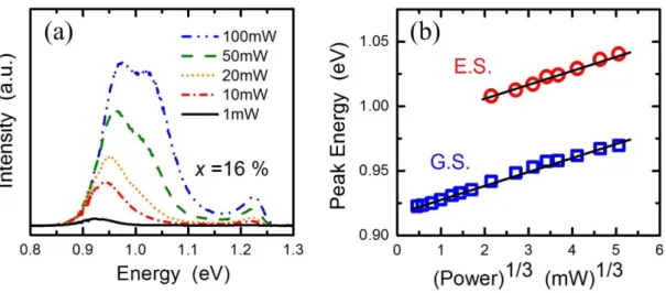
Figure 2.1 shows the PL spectra for the QD samples with different Sb compositions. A redshift in peak energy was observed with the increasing x. The power dependent PL spectra for the 16% sample are displayed in Fig. 2.2(a). Increasing the excitation power (Pex) results
13
Fig. 2.2: (a) Power dependent PL spectra of the 16% sample. (b) The GS and the ES peak energies as a function of Pex1/3 for the 16% sample.
in a blueshift in QD emission peaks. The energy shift shows a linear dependence on Pex1/3
[see Fig. 2.2(b)], consistent with the behavior expected for a type-II band alignment [42,54]. The PL peak can thus be identified as the recombination of ground-state (GS) electrons in the QDs with holes in the GaAsSb layer confined by the field induced band bending surrounding the QDs. The QD excited state (ES) appeared under higher Pex’s. A similar power
dependence of the blueshift was also observed for the QD ES.
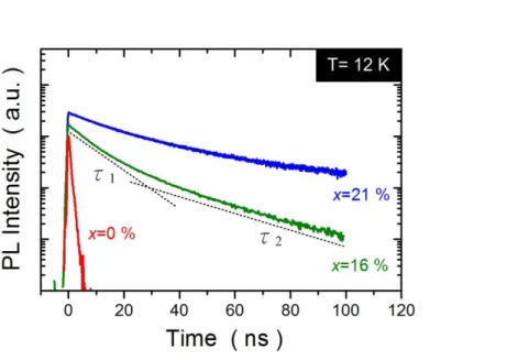
Figure 2.3 shows the TRPL of the investigated samples measured at T =12 K. The decay time for the reference InAs/GaAs QDs was τ ≈ 0.8±0.2 ns, comparable with the reported typical value of ~1 ns [55]. In contrast, the GaAsSb covered QDs exhibit much longer decay times than the reference InAs QDs. This can be attributed to the reduced spatial overlap between the electron and hole wavefunctions due to the type-II band alignment [56]. We notice that the decay traces for the GaAsSb covered QDs are non-single-exponential,
14
Fig. 2.3: TRPL decay traces for the GaAs1-xSbx capped InAs QDs with different x.
which can be decomposed into a faster initial component and a slower tail component. In order to obtain decay time constants, they are fitted by a double exponential function:
( )
For the 16% sample, the deduced time constants are =7.5 ns and =24 ns, with a relative ratio of A2/A1=0.4. The time constants for the 21% sample are somewhat longer ( ≈ 8.2 ns
and ≈ 29 ns), with a more pronounced slower decay component (A2/A1≈ 0.5).
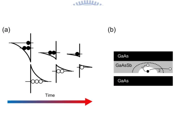
Similar non-single-exponential decays have been observed in GaSb/GaAs type-II QDs [57,58]. A quite general picture considering a time-dependent recombination rate of nonequilibrium carriers has been established and the schematic illustration is shown in Fig. 2.4. For the GaAsSb covered InAs/GaAs QDs investigated here, the underlying processes can be understood as follows. After the carrier excitations, electrons are captured rapidly into the QDs, exhibiting a band bending in the surrounding. On the other hand, holes are captured into
15
Fig. 2.4: (a) The schematic illustration of a time-dependent recombination rate of non-equilibrium carriers. (b) The sample structure and the underlying recombination processes responsible for the faster (1) and the slower (2) decay components.
the GaAsSb quantum well (QW) and then attracted by the nonequilibrium electrons. The induced band bending tends to confine the hole closer to the QDs and hence increases the electron-hole wavefunction overlap. The faster initial decay time can thus be related to the short-range radiative recombination of the QD electrons with the holes confined in the surrounding band bending. As the nonequilibrium electrons recombine continuously, the band bending reduces, leading to a reduced wavefunction overlap and hence a lower recombination rate. The band-bending effect would eventually become negligible when most of the nonequilibrium carriers have recombined. The longer decay time thus reflects the
long-range radiative recombination of the QD electrons with the holes in the GaAsSb QW
16
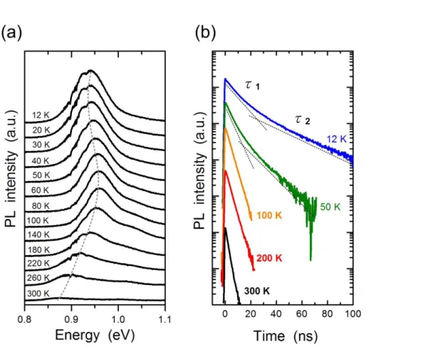
Fig. 2.5: Temperature evolution of the PL spectra (a) and decay traces (b) for the x=16% sample.
2.1.3 Temperature-dependent measurements
As elucidated above, the effect of nonequilibrium carriers is expected to be negligible under lower excitation conditions [57]. However, we found that the PL decay traces are still non-single-exponential even though the initial carrier density N0 was reduced
to less than 1 electron/dot. To further clarify this point, temperature dependent TRPL has been performed. The results for the x=16% sample are displayed in Fig. 2.5. In this study, the
Pex was kept low so that only the GS peak was observed (i.e., N0 2 electrons/dot). We found
17
typical feature of carrier localization effect and has already been observed in many alloy systems, such as InGaN/GaN and GaInNAs/GaAs QWs [59,60]. Because no S-shaped feature was observed in the reference InAs/GaAs QDs, the carrier localization must be in the GaAsSb CL, due possibly to alloy fluctuations and/or Sb clustering.
By comparing the S-shaped feature with the temperature dependent decay traces, the carrier dynamics of the non-single-exponential decay become clear. As shown in Fig. 2.5(b), the slower decay component was observed only at T<100 K. Because photogenerated holes are trapped by the localization states in the GaAsSb QW at low temperatures, they are less mobile and unable to be attracted into the bend-bending region induced by the QD electrons. This explains why the slower decay component can be observed at T<100 K even under low excitation conditions. With the increasing T from 30 to 100 K, these trapped holes gain thermal energy and start to populate the two-dimensional (2D) state of the GaAsSb QW. As the temperature was further increased, most of the holes were delocalized to the 2D QW state and hence could be efficiently attracted into the bend-bending region. Accordingly, the decay traces exhibit a well-defined single decay time constant at T 100 K, as expected for low excitation conditions.
Quantitatively, the hole localization energy can be deduced from the S-shaped energy shift. By using the relation combining the Varshni equation and localization effect [61],
( ) ( )
( )
, with parameters E0=0.998 eV, =11×10−4 eV/K, =600 K, and a localization energy ≈14
meV, a reasonable fit can be obtained [solid line in Fig. 2.6(a)]. An Arrhenius plot of the time-integrated intensities of the faster ( ) and the slower ( ) decay components obtained from the TRPL traces is shown in Fig. 2.6(b). In the range of T=30–100 K (the shadow region), I2 decreases while I1 increases in such a way that the total intensity
18
Fig. 2.6: (a) The PL peak energy as a function T. Lines are fitting curves with (solid) and without (dashed) localization effects. (b) An Arrhenius plot of the time-integrated intensities for the faster (I1) and the slower (I2) decay components.
I1+I2 remains nearly constant. Such intensity changes clearly elucidate the carrier transfer
process: the trapped holes are gradually delocalized by thermal energy and attracted into the bend-bending region surrounding the QDs. The activation energy for I2 was found to be
EA≈18 meV, close to the deduced localization energy . For T 100 K, the faster time
constant is =3.3±0.4 ns and is insensitive to T, as expected for well-confined zero-dimensional carriers. The time constant1 is approximately four times longer than the reference InAs QDs, corresponding to an electron-hole wavefunction overlap of ~50% of the type-I QDs. This value is considerably larger than that expected for a type-II exciton [56]. The appreciable overlap may be enhanced by the quantum confinement of the GaAsSb/GaAs QW. In addition, the small band discontinuity between InAs and GaAs0.84Sb0.16 is also
responsible for such an appreciable overlap.
1
The measured at T~100 K can be approximated as the actual recombination lifetime because both the temporal PL shift caused by the nonequilibrium electrons and the hole localization effect are less significant. For
T>200 K, however, the rapid decrease in the integrated PL intensity indicates that the nonradiative processes are
19
In summary, carrier dynamics of type-II InAs/GaAs QDs covered by a thin GaAsSb layer have been investigated by TRPL measurements. Different recombination paths in such type-II QDs have been clarified by temperature dependent measurements. The long-range recombination with the holes trapped by localized states in the GaAsSb QW is significant at low temperatures. At higher temperatures, the recombination is dominated by the holes confined to the band bending region surrounding the QDs.
20
2.2. RAPID THERMAL ANNEALING
Tailoring of the band alignment, the wave function overlaps and hence the carrier dynamics in InAs/GaAs1-xSbx QDs is necessary for practical applications. In particular, it has
been pointed out that the VB discontinuity plays an important role in the design of multiple transition solar cells. The use of antimony in the CL could have a strong advantage in obtaining a negligible VB offset, which is thought to be one of the key challenges in the development of QD-based solar cells. In principle, this can be done by varying the Sb composition in the GaAs1-xSbx layer to change the VB discontinuity at the InAs- GaAs1-xSbx
interface. However, alloy fluctuations and Sb clustering were usually accompanied with the increasing Sb content, making the QD’s optical properties even hard to control. An alternative approach is the use of postgrowth thermal annealing to smooth the VB discontinuity at the InAs/GaAs1-xSbx interface by the annealing induced alloy intermixing.
In this section, we employed PL and TRPL spectroscopes to investigate the emission properties of the InAs/GaAs1−xSbx type-II QDs after thermal annealing at temperatures
ranging from 700 to 900 °C. The annealing induced changes in the band alignment, the carrier dynamics, and electronics structures due to the alloy intermixing were observed and discussed.
2.2.1 Experimental details
Self-assembled InAs QDs were grown by MBE on GaAs substrates. The type-II QDs were formed by depositing 2.7 ML of InAs on a 200 nm thick GaAs buffer layer at 500 °C and subsequently capped by a 4.5 nm GaAs1−xSbx layer with a nominal x=0.16. A sample
with GaAs covered InAs QDs was also grown as a reference of type-I QDs. Atomic force microscopy of uncapped samples reveals that the QDs are lens shaped, with an average height of ≈8±0.5 nm, a diameter of ≈20 nm, and a density of 3×1010 cm−2. Finally, the QDs
21
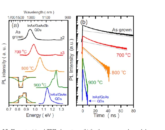
Fig. 2.7: PL spectra (a) and TRPL decay traces (b) for the as-grown and annealed InAs/GaAsSb QDs, together with the reference InAs/GaAs QDs.
were capped by a 50 nm GaAs layer. Postgrowth rapid thermal annealing for the GaAsSb covered sample was performed at annealing temperatures TA ranging from 700 to 900 °C for
20 s using GaAs proximity capping.
2.2.2 Effects of thermal annealing on the emission properties
Figure 2.7(a) shows the PL spectra for the as-grown and the annealed QD samples measured at 10 K under a low excitation power of 0.5 mW. The PL spectrum for the type-I InAs/GaAs QDs is also shown for comparison. With the increasing TA, a blueshift and a
22
narrowing of the QD’s emission peak were observed [62-67]. The energy blueshift is caused by the alloy intermixing between the QDs and barrier materials, which shallows the QD’s confining potential due to the incorporation of more Ga atoms into the InAs QDs [62-67]. For the as-grown sample, it has been confirmed in our previous study (Sec. 1 in this chapter) that the InAs/GaAs0.84Sb0.16 QDs exhibited a type-II band lineup, where the radiative
recombination occurs between the electrons confined in the QDs and the holes in the GaAsSb layer. Annealing induced alloy intermixing also tends to smooth the VB discontinuity at the InAs–GaAsSb interface. Therefore, the electron-hole wave function overlaps and hence the radiative recombination rate is expected to be enhanced or even changed gradually to type-I transitions after thermal annealing.
To understand the effects of thermal annealing on the recombination dynamics in the type-II QDs, TRPL measurements have been performed and the results are shown in Fig. 2.7(b). The PL decay time was found to decrease with the increasing TA, indicative of a more
penetrated hole wavefunction into the InAs QDs due to the reduced VB offset caused by alloy intermixing at the InAs–GaAsSb interface. In particular, we found that the decay transient for the 900 °C annealed QDs became as fast as the InAs/GaAs type-I QDs. This implies that the QD structure has been changed to a type-I band alignment after high-temperature annealing.
In principle, the recombination lifetime can be quantitatively deduced from the measured PL decay transients. However, the determination of recombination lifetime is not straightforward for a type-II system. One complication arises from the effect of nonequilibrium carriers: as the carriers recombine continuously, the PL shifts to lower energies due to the reduced VB bending surrounding the QDs. Therefore, the decay transient recorded at a given wavelength does not reflect the true lifetime since the PL decay arises not only from the carrier recombination but also from the temporal PL shift. For the InAs/GaAsSb material system, the carrier dynamics is further complicated by the presence of
23
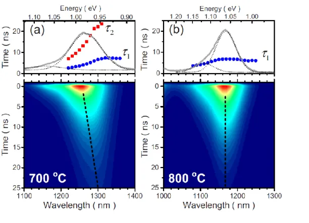
Fig. 2.8: Energy dependent carrier lifetimes and time evolution of the PL spectra for the samples annealed at (a) 700 °C and at (b) 800 °C.
localized hole states in the GaAsSb layer due to alloy fluctuations and/or Sb clustering. The redistribution of holes among these localized states also significantly influences the overall carrier dynamics, particularly at low temperatures. In order to clarify the role of both effects (i.e., the nonequilibrium carriers and the localized states) in the PL transients, energy dependent TRPL has been performed. The results for the 700 and 800 °C annealed QDs are shown in Figs. 2.8(a) and 2.8(b), respectively. For the 700 °C annealed QDs, a clear temporal PL redshift can be observed. Since the excitation power was kept low, the effect of
24
nonequilibrium carriers is expected to be less significant. In fact, an even more pronounced temporal PL shift was observed for the as-grown sample. Thus we ascribe the temporal PL redshift to the effect of hole localizations in the GaAsSb layer. On the contrary, the temporal PL redshift was absent for those QDs annealed at TA≥800 °C. This indicates that the localized
hole states have been removed by the annealing induced alloy intermixing. The temporal PL redshift is closely related to the nonsingle exponential decay observed in PL transients shown in Fig. 2.7(b). Investigations of all samples revealed that the temporal PL redshift can be observed only when the decay transient is nonsingle exponential. By using a double exponential function ( ) to fit the PL decay recorded at each wavelength, the decay time constants and for the faster and the slower decay components can be obtained. The fitted results are shown in the upper panel of Fig. 2.8, along with its time integrated PL spectrum. For the 700 °C annealed QDs, both and show strong energy dependences, indicative of hole transfers among localized states in the GaAsSb layer. For the 800 °C annealed QDs, we found that is almost unchanged across the ground state emission band.
25
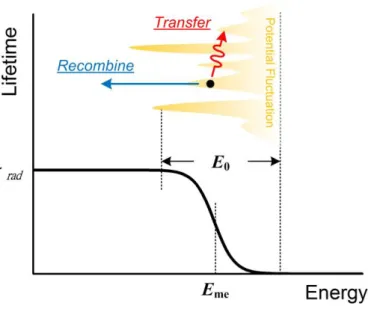
Fig. 2.9: The schematic illustration of hole redistribution among fluctuant potentials and the corresponding energy dependent lifetime.
The energy dependent lifetime can be described by ( )
, where is the radiative lifetime, E0 describes the localization depth, and Eme is the
energy similar to the mobility edge [68]. The schematic illustration of hole redistribution among fluctuant potentials and the corresponding energy dependent lifetime are shown in Fig. 2.9. As shown in the figure, carriers in shallower potentials are with higher probability of transfers, thus, resulting in shorter lifetimes. On the other hand, carriers in deeper potentials tend to recombine and the measured lifetimes are closer to radiative lifetimes.
26
Fig. 2.10: Radiative recombination rate as a function of the annealing temperature. The data from the as-grown sample are plotted at 500 °C.
Figure 2.10 shows the radiative recombination rate ( ) deduced from the energy
dependent lifetime for all annealed samples. The measured increases slightly from 0.095 ns−1 for the as-grown sample to 0.15 ns−1 after annealing at TA=800 °C, but still about
an order of magnitude lower than the InAs/GaAs type-I QDs (1.25 ns−1). The low recombination rates indicate that their band lineups remain type-II, with an electron hole wave function overlap of only ~28%–35% of the type-I QDs. As TA was increased to 900 °C,
the recombination rate increases dramatically to =1.2 ns−1, which is very close to that of
27
2.2.3 The evolution of band alignments
In order to examine whether the QDs are still present after high-temperature annealing, rather than evolving into a quantum-well-like structure, we have also measured the power-dependent PL spectra for the annealed samples. Figure 2.11 shows a comparison among the power-dependent spectra for the QDs annealed at 700, 800, and 900 °C. With the increasing excitation power (Pex), higher energy peaks become observable for all samples due
to the state-filling effect, which is a feature specific to a zero-dimensional system [63,65-67]. This demonstrates unambiguously that the annealed structures remain as QDs even after 900 °C annealing. The peak energy shifts in the power-dependent spectra also provide evidences for the band alignment changes after thermal annealing. For the 700 °C annealed QDs, the QD peaks shift linearly with , i.e., a fingerprint of type-II transitions. This feature is not observed for the QDs annealed at 900 °C, confirming their type-I alignment. The most interesting is the case annealed at 800 °C, where the peak blueshift is observed at lower excitation powers but becomes nearly unchanged for Pex>5 mW. This behavior can be
explained by an evolution from the type-II to type-I recombination induced by the large VB bending surrounding the QDs. After 800 °C annealing, the VB offset at the InAs-GaAsSb interface has been reduced by the alloy intermixing. To confine holes around the QDs and retain a type-II recombination, the VB bending should be weak and the excitation power must be low. When a large amount of nonequilibrium electrons was injected into the QDs by a higher Pex, a very strong VB bending will exhibit in the QD surrounding. This makes the
small VB offset unable to support confined hole states in the QD surrounding, leading to a gradual evolution from a type-II to a type-I transition.
28
Fig. 2.11: Power dependent PL spectra for the samples annealed at (a) 900 °C, (b) 800 °C, and (c) 700 °C. (d) The peak energy of QD ground state as a function of Pex1/3.
In summary, the emission properties of the InAs/GaAs1−xSbx type-II QDs after
thermal annealing have been investigated. Apart from large blueshifts and a pronounced narrowing of the QD emission peak, alloy intermixing also lead to enhanced recombination rates and reduced localized states in the GaAsSb layer. The type-II QD structure has evolved into a type-I alignment after 900 °C annealing. We found that it is possible to manipulate between type-I and type-II recombinations in annealed QDs by using different excitation powers. We demonstrated that post growth annealing can be used to tailor the band alignment, the wavefunction overlaps, and hence the recombination dynamics in the InAs/GaAsSb type-II QDs.
29
2.3. MODULATION OF CAPPING LAYER THICKNESS
Variation of the Sb content in the GaAsSb CL (Sec. 1 in this chapter) and post-growth thermal treatments (Sec. 2 in this chapter) have been employed to tailoring the transition energy, the band alignment, the wave function overlaps and hence the carrier dynamics for specific applications. Another approach is to change the GaAsSb CL thickness, which is expected to affect the quantum confinement of hole states and the strain distribution surrounding the type-II QDs. Furthermore, GaAsSb CL with appropriate thickness is essential for applications with stacked multilayer structure. However, not much attention has been paid to the evolution of optical properties of the GaAsSb-capped InAs/GaAs QDs with the CL thickness.
In this section, we investigate the evolutions of emission energy and recombination lifetime of the GaAsSb-capped InAs/GaAs QDs with the CL thickness. The effects of the CL thickness on the hole states and their wave function distributions are discussed and compared with eight-band k⋅p model calculations.
2.3.1 Experimental details
The samples were grown by MBE. A layer of self-assembled InAs QDs (2.7 MLs) were grown at 500 °C on the GaAs buffer layer and subsequently capped by a GaAs0.8Sb0.2 layer
with a thickness t. Four samples with t= 0, 2.5, 5 and 10 nm have been grown. The samples were finally capped by a 50 nm GaAs layer. Atomic force microscopy revealed that uncapped surface QDs are lens shaped, with an average height of 8.0 ± 0.5 nm, an average diameter of 20 nm, and an areal density of about 3×1010 cm-2.
30
Fig. 2.12: The PL spectra measured at T= 12 K for the investigated QD samples with different CL thickness t.
2.3.2 Effects of GaAsSb capping layer thickness on the optical properties
Figure 2.12 shows the PL spectra measured at T= 12 K for the QD samples under a low excitation power (Pex=10 μW). A clear redshift of the PL peak with the increasing GaAsSb
CL thickness is observed. For the nominal Sb content of x = 0.2 in the CL, the InAs-GaAsSb interface is expected to exhibit a type-II band alignment. Therefore the PL redshift with the increasing CL thickness can be attributed to the combined effects of the formation of type-II QDs, the reduced quantum confinement of the hole states, as well as the modifications in the strain distribution in the CL layer. Besides, the GaAs1-xSbx capping (with x > 0.2 ) could
increase in the dot height due to the suppressed QD decomposition. However, the evolution of QD size with the GaAsSb CL thickness remains unknown. To gain information about the structural changes by the GaAsSb capping, cross-sectional transmission electron microscopy (TEM) have been performed, which are shown in Fig. 2.13. For the GaAs-capped QDs, the islands are flat in shape, with dimensions of about h= 2.5 nm in height and d= 18 nm in
31
Fig. 2.13: The cross-sectional TEM images for the samples with different CL thicknesses.
diameter. After the GaAsSb capping, a gradual increase in the QD size with the CL thickness is observed. The estimated heights (diameters) are 3.1 nm (21 nm), 4.1 nm (21 nm) and 5.2 nm (24 nm) for CL thickness t= 2.5, 5 and 10 nm, respectively. Although accurate determinations of the QD size and shape are hindered by the strong strain field contrast in the TEM images, a clear increasing trend of the QD size with the CL thickness can still be inferred. This means that the enlarged QD size should also be considered in the PL redshift with the CL thickness.
32
Fig. 2.14: Power-dependent PL spectra for the GaAsSb-capped samples with a CL thickness of (a) 2.5 nm, (b) 5 nm, (c) 10 nm. All the PL spectra have been offset and the intensities have been normalized to their ground-state peak. (d) The ground-state peak energy of the QDs as a function of Pex1/3.
To clarify the major effect of the CL thickness, we have performed power dependent PL measurements, which are shown in Fig. 2.14. For the GaAs-capped QDs, the ground-state peak energy remains nearly constant in the investigated power range. By contrast, the GaAsSb-capped samples with t= 5 and 10 nm show large blueshifts with the increasing excitation power, which are clear signatures of the formation of type-II QDs after GaAsSb capping. However, as the CL thickness was reduced to t= 2.5 nm, only a moderate blueshift
33
Fig. 2.15: (a) TRPL spectra and (b) the deduced decay time for the investigated QD samples with different CL thickness t.
of 15 meV is observed. This indicates that a thinner CL thickness tends to reduce the type-II character of the GaAsSb-capped InAs QDs.
The effect of CL thickness on the radiative recombination lifetime in the GaAsSb-capped QDs has also been investigated by TRPL measurements. For a type-II system, the spatially separated electrons and holes would increase the radiative recombination lifetime , which is inversely proportional to the square of the overlap integral of the electron and hole wave functions and proportional to the emission energy EPL , i.e.,
|⟨ ( )| ( )⟩|
, where ( )( ) is the electron (hole) wave function. Since ( ) is still well-confined in the QDs even after the GaAsSb capping, the measured can thus be a measure of the proportion of ( ) that remains in the QDs. Figure 2.15(a) shows the PL decay recorded at
34
the PL peak under low excitation conditions. The determined as function of CL thickness are shown in Fig. 2.15(b). For the GaAs-capped InAs QDs, we obtain = 0.77 ns, which is comparable to the value reported in literature. By contrast, a gradual lengthening of the PL decay time with the increasing CL thickness is observed for the GaAsSb-capped samples. The deduced are 1.9, 14 and 45 ns for the samples with t= 2.5, 5 and 10 nm, respectively. If we assume that ⟨ ( )| ( )⟩ in the type-I InAs QDs, the overlap in the GaAsSb-capped samples still has 58% for t= 2.5 nm, but decreases to 21% and 11% for t= 5 and 10 nm, respectively. This means that the hole wave function distribution in the GaAsSb layer is sensitive to the CL thickness, especially for t < 5 nm.
2.3.3 Simulations
Theoretical calculations based on eight-band k⋅p model [69] have been performed in order to understand the effects of CL thickness quantitatively. For a comparison purpose, we model the InAs QD as a truncated pyramid with {101} facets and having a conformal GaAs0.8Sb0.2 CL covering thereon with a thickness t. All the material parameters are adapted
from Ref. 70, except that the unstrained valence band offsets and the deformation potentials are obtained from Ref. 71 and 72. The strain-induced piezoelectric polarization has also been included. In order to separate the effects of CL thickness on the hole states and the enlarged QD size on the electron states, we have performed two sets of calculations. In the first set we considered a constant QD size (h= 3.5 and b= 14 nm) and varying the CL thickness from t= 0 to 10 nm. The calculated wave function distributions of the hole ground state on the (110) plane are displayed in Fig. 2.16(a) to (d). For the GaAs-capped QD, the hole is well-confined in the QD with a high wave function overlap up to 98%. With the increasing t, the hole wave function penetrates gradually into the GaAsSb layer due to the reduced quantum confinement of hole states in the CL. The hole wave function is localized close to the QD base, in consistent with recent calculations [73]. As t is further increased from 5 to 10 nm, the hole
35
Fig. 2.16: The calculated wave functions of the hole ground state of the InAs QD with a GaAsSb CL thickness of (a) 0 nm, (b) 2.5 nm, (c) 5 nm, and (d) 10 nm. (e) The electron-hole wave function overlaps and (f) the ground state transition energy as a function of the CL thickness, where the solid symbols are experimental data, while the solid curves (open symbols) are calculated results obtained from the first (second ) set of calculations.
wave function becomes more extended in the GaAsSb layer. On the other hand, the electron states, as well as their wave function distributions are nearly unchanged by the GaAsSb capping. As shown in Fig. 2.16(e), the calculated wave function overlap (solid curve) decreases gradually from t= 2 to 5 nm and become less dependent on the CL thickness for t > 5 nm, in agreement with the experimental data (solid symbols). In Fig. 2.16(f), the calculated transition energy also shows a redshift with the increasing CL thickness. The overall redshift from t= 0 to 10 nm is 140 meV, which is however smaller than the experimental redshift (~250 meV). In fact, we have also calculated different QD sizes (but keeping a constant size
36
Fig. 2.17: The RT PL spectra for the samples with a CL thickness of t = 0 and 2.5 nm.
for all t) and found that only minor changes in the overall redshift in the transition energy. This indicates that the different CL thicknesses, which affect predominantly the hole states, cannot fully account for the observed PL redshift. Therefore, in the second set of calculations, we further consider the enlarged QD size induced by the GaAsSb capping according to our TEM analysis. All other parameters are kept the same. As shown in Fig. 2.16(e) and 2.16(f), the experimental energy shift is well reproduced by the second set of calculations (open symbols). This result indicates that the modification in QD size by the GaAsSb capping still plays a nonnegligible role in the evolution of the optical property of the InAs QDs with CL thickness.
We would like to mention that the GaAsSb-capped sample with t= 2.5 nm exhibits a stronger PL intensity and a narrower PL linewidth at T= 12 K. This sample also shows a RT PL emission at 1.3 μm with a large enhancement in the integrated intensity (~7×) as compared with the GaAs-capped QDs [see Fig. 2.17]. Such an improvement in the optical properties is very appealing for long-wavelength emitters. Although the increased dot height of the GaAsSb-capped QDs is beneficial for extending the emission wavelength, the
37
formation of type-II QDs for higher Sb contents on the other hand hinders them from being efficient light emitters. A trade-off might be researched by optimizing the Sb content in the GaAsSb CL. The study suggests that a careful control of the GaAsSb CL thickness ( t < 2.5nm) is an alternative approach for extending the emission wavelength while retaining the type-I characters of the QDs.
In summary, we have used PL and TRPL measurements to study the emission energy and the recombination lifetime of GaAsSb-capped InAs QDs with different CL thicknesses. Theoretical calculations indicated that the PL redshift and the lengthening of PL lifetime arise not only from the modifications in the quantum confinement of hole states in the GaAsSb layer, but also from the Sb induced structural changes in the QDs. Controlling the GaAsSb CL thickness can be an alternative approach for tailoring the optical properties of GaAsSb-capped InAs QDs.