電子工程學系 電子研究所碩士班
碩 士 論 文
非對稱蕭特基能障薄膜電晶體與浮停閘極記憶
體元件之製作與特性分析
Fabrication and Characterizations of
Asymmetric Schottky Barrier Thin-Film
Transistors and Floating Gate Memory Devices
研 究 生: 林歷樺
指導教授 : 林鴻志 博士
黃調元 博士
體元件之製作與特性分析
Fabrication and Characterizations of
Asymmetric Schottky Barrier Thin-Film
Transistors and Floating Gate Memory Devices
研 究 生 : 林歷樺 Stduent: Li-Hua Lin
指導教授 : 林鴻志 博士 Advisors: Dr.Horng-Chih Lin
黃調元 博士 Dr.Tiao-Yuan Huang
國立 交 通 大 學
電子工程學系 電子研究所碩士班
碩 士 論 文
A Thesis
Submitted to Department of Electronics Engineering & Institute of Electronics College of Electrical and Computer Engineering
National Chiao Tung University In partial Fulfillment of the Requirements
for the Degree of Master in
Electronics Engineering June 2011
Hsinchu, Taiwan, Republic of China
非對稱蕭特基能障薄膜電晶體與浮停閘極記憶
體元件之製作與特性分析
研究生 : 林歷樺 指導教授 : 林鴻志 博士
黃調元 博士
國 立 交 通 大 學 電子工程學系 電子研究所碩士班摘要
在本論文中,我們利用一種新穎且低成本的雙重微影成像技術成功地製作出 非對稱蕭特基能障薄膜電晶體。這個方法需要利用I-line 光學步進機進行兩次的 微影曝光以及後續的蝕刻步驟來定義出實際的閘極圖案,這樣的一個方式不僅有 機會將閘極長度微縮至奈米尺度而且還能將元件的源極/汲極接面製作成非對稱 式結構。這個新穎的非對稱蕭特基能障薄膜電晶體在順向模式的操作下是以矽化 鎳(NiSi)蕭特基接觸當作源極而磷離子摻雜區域當作汲極,如此一來可以明顯地 降低漏電流並且有效地減緩雙極性導通的現象。除此之外,一個兩段式斜率的次 臨界電流-電壓特性也被觀察到,電荷載子的注入機制在此將被分析解釋。當利 用矽化鎳當作源極,我們將研究由於陡峭的能帶彎曲引發的源極端的熱電子注入 現象。顯著的閘極電流以及負電阻現象可以同時被觀察到,這被認為是源極端產 生的熱電子被注入氧化層並且動態地被陷補所致。 以這個獨特的非對稱蕭特基能障結構為基礎,我們也成功地製作並分析浮停 閘結構的快閃記憶體元件。因為源極端具有陡峭蕭特基能障,因此可以誘發熱電 子並且在低電壓操作下被高效率地由源極端注入浮停閘,這與傳統的汲極端熱電 子注入是不同的。相較於傳統的薄膜電晶體浮停閘記憶體元件,非對稱蕭特基能 障薄膜電晶體浮停閘元件在低電壓操作下展現了較高的寫入速度。Fabrication and Characterizations of
Asymmetric Schottky Barrier Thin-Film
Transistors and Floating Gate Memory Devices
Student : Li-Hua Lin Advisors : Dr. Horng-Chih Lin Dr. Tiao-Yuan Huang
Department of Electronics Engineering and Institute of Electronics National Chiao Tung University, Hsinchu, Taiwan
Abstract
In this thesis, asymmetric Schottky barrier (ASSB) thin film transistors (TFTs) are successfully fabricated by utilizing a novel and low-cost double patterning technique. The method involves twice the lithography with an I-line stepper and subsequent etching process steps to define the real gate pattern, which is not only a promising scheme for achieving nanoscale gate length but also feasible for fabricating devices with asymmetric source/drain (S/D) junctions. The novel ASSB-TFT devices operated in forward mode featuring a NiSi Schottky contact at the source side and a phosphorous-doped drain can significantly lower leakage current and thus the ambipolar conduction is largely mitigated. Moreover, a two-step subthreshold transfer characteristic is also observed and the carrier injection mechanisms are analyzed. When the NiSi layer is used as the source, the phenomenon of a source-side hot electron injection triggered by the sharp energy band bending is investigated. A large gate current and the negative-differential conductance (NDC) behavior are simultaneously observed, which is attributed to hot electron generated at the Schottky source side and dynamic hot electron trapping in the oxide.
Based on this unique ASSB structure, floating-gate (FG) device for Flash memory is also successfully fabricated and characterized. The sharp Schottky barrier at the source side can induce hot electrons, and it can be used to provide high injection efficiency at low voltage rather than conventional drain-side channel hot electron injection. Compared with a conventional TFT-FG memory device, the ASSB TFT-FG memory device exhibits high-speed programming at low voltage.
Acknowledgement
寫下致謝的當下,代表將近兩年的碩士生涯也就將畫下句點。從無到有,是 一個個漫長的過程,也不是只靠我一個人就可以完成這本碩士論文。我很幸運, 在這一路上總是遇到願意支持我、幫助我的人。能夠走到這邊,心中的感謝不是 三言兩語就可以表達,許多人的過去的幫忙點滴都在心頭。 首先,我要特別感謝我的兩位指導老師,黃調元博士與林鴻志博士。黃老師 在教學上總是將半導體的觀念說明的特別清楚而且有趣,啟發了我對於半導體的 興趣。而平常黃老師態度親切,也讓我跟老師相處起來沒有壓力。林老師在實驗 上總是不吝與我討論問題所在,並且常常從老師身上看到對於學術的熱情,這樣 的態度也總是鼓舞我,也激勵人產生更多的動力繼續往前。我想兩位老師對我的 影響,不僅僅是在研究上,而是一種態度的潛移默化,這將是我最大的收穫。 接下來我要感謝實驗室的成員,因為他們的協助,讓我可以更順利的進行實 驗。第一次做實驗帶領我的陳威臣學長,無論是蝕刻還是曝光,不厭其煩地進到 無塵室帶我做實驗。還有討論問題和實驗現象時候,總是可以提出精闢的見解, 讓我得到許多寶貴的學習經驗。而林哲民學長帶領我做碩士論文的題目,每個製 程流程與每個細節都一起參與,以及電性量測上給予許多寶貴的建言,因此這個 實驗特別順利,最終也有個成果。而且每當我灰心喪志,失去信心的同時,你總 能給予希望,讓我知道我們的努力不會是白費的,真的很謝謝你。再來,實驗室 的學姊李克慧會與我分享生活的點滴,聊聊女生的話題,分享好看的電影跟韓 劇,生活中多了樂趣。蔡子儀學長在無塵室的許多幫忙,還有製程上的指導,讓 我的實驗更得以順利完成。徐行徽學長、郭嘉豪學長,還有林政頤學長也在我實 驗上提供建議或者協助,這些我也將銘記在心。而同屆的嘉文,雖然沒有一起經 歷碩二的奮鬥時光,但未來還請多關照。 在 631 的成員,俊鵬在我第一次做實驗什麼都不懂的情況下,以過來人的身 分給我許多幫忙,也指導我製程上的操作,讓我可以很快上手。段凱經常解決我 在電腦上的問題,能夠幫忙的地方你也總是不吝於付出。宇賢、崇名、同偉、孝 雄是我碩士生涯的夥伴,大家一起有個目標往前進,不論在實驗上或者生活上都 將是珍貴的回憶與成長。 還在 628 的學弟妹,梵懿、曉惠、維真各個都是貼心好女孩,讓這個實驗室 多了許多歡樂跟笑聲。涵宇、盈宇、廷燿很好相處,寒假一起出遊帶給我有趣的 回憶。 最後,我要感謝家人,爸媽在物質上讓我毫無後顧之憂,而且總是支持我想 做的任何事情,讓我得以任性的下任何決定。姐姐和哥哥平日在生活上的噓寒問 暖,親情的溫暖也是在外遇到挫折時的依靠。 這本論文的完成,是一個階段的結束,但是曾經的共有的時光卻將是永存在 心。CONTENTS
Abstract (Chinese)……….i
Abstract (English)………ii
Acknowledgement………...iv
Contents……….v
Table Captions………vii
Figure Captions………..vii
Chapter 1 Introduction……….1
1.1 Schottky Barrier MOSFET………...1
1.2 Overview of Nonvolatile Memory………....……...3
1.2.1 Floating Gate Flash Memory………4
1.2.2 Nor Flash………..5
1.2.3 Reading Operation………...6
1.3 Motivation……….……..……...6
1.4 Thesis Organization………...….……..……...8
Chapter 2
Process Technology, Device Fabrication,
Measurement Setup, and Carrier Transport Mechanisms…9
2.1 Review of Asymmetric Schottky Barrier Transistors...92.2 Double Patterning Technique………...10
2.3 Ni-Silicide……….……..……...11
2.4.1 Process Flow of ASSB-TFT Devices………12
2.4.2 Process Flow of ASSB-TFT-FG Memory Devices………...13
2.5 The Measurement Setup………..14
2.6 Charge Injection Mechanisms……….14
2.6.1 Channel Hot Electrons Injection………...15
2.6.2 Fowler-Nordheim Tunneling………..17
2.6.3 Band-to-Band Tunneling………...18
2.6.4 Summary………..18
Chapter 3 Results and Discussion………..20
3.1 Fundamental Electrical Characteristics……….20
3.2 Source-side Hot Electron Injection……….23
3.3 Program Characteristics of ASSB-FG Memory………28
3.4 Discussion………...30
Chapter 4 Conclusions and Future Work………..32
4.1 Conclusions………. ……….32
4.2 Future Work………..33
References………35
Table Captions
Chapter 1
Table 1-1 Advantage of SB-MOSFFT over Conventional MOSFET...8
Figure Captions
Chapter 1
Fig. 1-1 Ambipolar conduction of the Schottky barrier device……….41 Fig. 1-2 The Band diagrams along the channel of an n-type SB device from
source to drain when gate voltage is negatively biased……….41 Fig. 1-3 Cross-sectional view of the proposed TFT device [15]………....42 Fig. 1-4 Detailed subcategories of RAM and ROM memory families[16]…...42 Fig. 1-5 Schematic cross section of a FG memory [18]………...43 Fig. 1-6 The reading operation of FG memory [18]………43 Fig. 1-7 Schematic illustration of the logical state which can not be successfully
read………44 Fig. 1-8 Schematic illustration of the normal reading operation of
memory………...44
Chapter 2
Fig. 2-1 The cross-sectional view of the rinsed asymmetric Schottky barrier PMOS process sequence and the finished structure [25]……….45 Fig. 2-2 The top view of the double patterning layout. The gate region is
determined by the overlapped portion of the two masks……….46 Fig. 2-3 Illustration explains silicon consumption………...46 Fig. 2-4 Process flow of ASSB TFT. (a) α-Si layer deposition and SPC on wet oxide. (b) After defining the active region, deposition of TEOS gate oxide and in-situ doped poly gate. (c) G1 mask definition and drain side implantation. (d) After stripping of PR, deposition of hard mask. (e) Defining the real gate region by G2 mask. (f) Deposition of nitride film and then sidewall spacer formation by RIE. (g) Formation of NiSi at source side……….47 Fig. 2-5 The cross-sectional view of conventional n-type TFT structure……..48 Fig. 2-6 The cross-sectional view of ASSB-FG TFT memory………...48 Fig. 2-7 The cross-sectional view of conventional n-type FG TFT memory….49 Fig. 2-8 (a) Channel hot electrons caused by strong lateral electrical field in
pinch-off region. (b) Hot electrons gain sufficient energy and are injected into gate...50 Fig. 2-9 Electrons are “heated” by the high lateral electric field. The energy
distribution is a function of lateral field. Each of these functions needs to be specified in each point of the channel [35]………51 Fig. 2-10 (a) Fowler-Nordheim tunneling occurs when ox
ox q E t ( ox ox ox V E t ) (b) Direct tunneling occurs when oxide is thin enough………...51 Fig. 2-11 Band-to-Band Tunneling (BTBT) (a) Deep depletion appears in n+
drain region overlapped by gate. (b) Main tunneling mechanism occurs in deep depletion region………...52
Chapter 3
And reverse operation modes, respectively………..54 Fig. 3-2 Transfer characteristics of ASSB-TFTs under forward operation
modewith channel length of (a) 0.5 μm and (b) 1 μm………...54 Fig. 3-3 Conceptual energy diagrams and transfer characteristics of silicided-
source SB-MOSFETs to explain the dominant carrier injection mechanisms ……….55 Fig. 3-4 Transfer characteristics of ASSB-TFTs under forward operation mode
with oxide thickness of 10nm, 15nm and 20 nm .. ………56 Fig. 3-5 Transfer characteristics of ASSB-TFTs operated in both modes
together with those of the conventional n-type TFT structure for comparison………56 Fig. 3-6 Energy band diagrams of conventional SB-MOSFETs at various bias
conditions. (a) no voltage is applied to the drain and the gate and thus no any current can tunnel through Schottly barriers. (b) At the on-state (Vgs>0, Vds>0), electrons can easily tunnel through the thinner source-side SB. (c) At the off-state, holes can easily tunnel through the thinner drain-side SB, leading to GIDL-like current………...57 Fig. 3-7 Energy band diagrams of n-type ASSB-TFT device at various bias
conditions.(a) no voltage is applied to the drain and the gate and thus no any current can be observed. (b) At the on-state (Vgs>0, Vds>0), electrons can easily tunnel through the thinner source-side SB. (c) At the off-state, the n+ Si band gap effectively block hole tunneling………58 Fig. 3-8 The cross-sectional view of p-type ASSB-TFT structure………..59 Fig. 3-9 Transfer characteristics of p-type ASSB-TFT operated in both
modes……….59 Fig. 3-10 Transfer characteristics of p-type and n-type ASSB-TFT operated in
forward modes...……….60 Fig. 3-11 Gate current versus drain voltage characteristics as a function of gate voltage operated in forward mode………..60 Fig. 3-12 Schematic illustration of the energy band diagram for both the
ASSB-TFT device and the conventional device along the channel direction………...61 Fig. 3-13 Output characteristics of an ASSB-TFT operated under forward
mode...62
Fig. 3-14 Sub-threshold transfer characteristics of an ASSB-TFT operated in forward modes before and after dynamic electrontrapping…………62 Fig. 3-15 Gate current versus drain voltage characteristics as a function of gate voltage for an ASSB-TFT operated in reverse mode………63 Fig. 3-16 Gate current versus drain voltage characteristics of a conventional
device as a function of gate voltage………...63 Fig. 3-17 Output characteristics of an ASSB-TFT in reverse mode and a conventional control device. The gate length L and width W are 1 and 10 um, respectively………...64 Fig. 3-18 Output characteristics of an ASSB-TFT in reverse mode. The gate
length L and width W are 5 and 10 um, respectively………64 Fig. 3-19 Schematic illustrations of the charge injection points for source-side
hot electrons (a) and FN tunneling (b)………...65 Figs. 3-20 Gate current versus drain voltage characteristics as a function of gate
voltage for an ASSB-TFT under forward operation mode with channel lengths of (a) 0.5μm (b) 1μm (c) 2μm (d) 5μm (e)
10μm………..65 Figs. 3-21 Gate current versus drain voltage characteristics for ASSB-TFTs with
various channel lengths at the Vg of (a) 5V, (b) 6V, (c) 7V, and (d) 8V, respectively………68 Fig. 3-22 The plot of gate current versus channel length as a function of Vg at Vd = 0V………..70 Fig. 3-23 Gate current versus drain voltage characteristics of ASSB-TFT
devices with oxide thickness of 10nm and 15 nm, respectively……..70 Fig. 3-24 Comparisons of gate current for an ASSB-TFT operated in two modes, together with its conventional control device……….71 Fig. 3-25 Transfer characteristics of an ASSB-FG device before and after
programming operation………..72 Fig. 3-26 Programming characteristics of ASSB-FG memory devices with
different drain biases and Vg = 8V………...72
Fig. 3-27 Programming characteristics of (a) ASSB-FG memory and (b) conventional FG memory with different bias conditions………...73
Fig. 3-28 Cross-sectional TEM image of the ASSB-FG memory device along the channel direction. From the high-solution inset, it can be seen that an offset region exists between the NiSi source and the poly-Si channel (indicated by the double-head arrows)………...74
Chapter 1
Introduction
1.1 Schottky-Barrier MOSFET
The concept of Schottky-barrier metal–oxide–semiconductor field-effect transistors (SB-MOSFETs) which replace the heavily impurity-doped silicon in source/drain (S/D) regions with metallic material, typically silicides, was first proposed by Nishi in 1966. Japanese patent on the schottky barrier S/D was issued in 1970 [1].The first SB-MOSFET device was successfully fabricated by Lepselter and Sze in 1968, utilizing PtSi for the S/D regions [2]. Compared with conventional MOSFETs with the PN S/D junctions, the SB-MOSFETs have several favorable advantages such as short-channel effect (SCE) immunity, low extrinsic parasitic resistance, low thermal budget in fabrication, and superior scalability due to the atomically abrupt junctions formed at the silicide–silicon interface [3-4].The silicided junction depth can be narrowly controlled by the deposited metal thickness and annealing conditions (temperature and duration). Table 1-1 summarizes the characteristic comparison between SB-MOSFETs and conventional MOSFETs. In 1983, the SB pMOSFET was verified to eliminate the latch-up effect [5-6]. Nowadays, SB-MOSFETs have attracted much attention as promising candidates in future ultra-large-scale integrated circuit (ULSI) devices [7-8]. Furthermore, since the S/D formation is implemented at low temperature, typically below 600℃, the metal gate and high-k gate dielectric technologies can be viably incorporated in SB-MOSFETs [3].
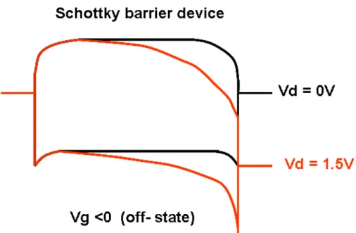
less steep switching characteristics than conventional MOSFETs. It is found that the Schottky barrier height (SBH) significantly affects the series resistances.For typical SB-MOSFETs, the on current is limited by carriers tunneling through the SB at the source end of the channel.A very low or even a negative SBH at source-side is favorable for the on-current to reach a comparable performance as conventional MOSFETs [9]. Also, SB-MOSFETs show ambipolar behavior if the barrier height for minority carrier at drain-side is not sufficiently high, which yields large and bias-dependent off-state leakage current [10], as shown in Fig. 1-1. The large leakage current attributed to hole (electron) tunneling from the drain side of n-type SB (p-type SB) devices can be a serious issue even with a high driving current. Figure 1-2 shows the band diagrams along the channel of an n-type SB device from source to drain when gate voltage is negatively biased.
In order to deal with the thorny problems of SB-MOSFETs mentioned above, it is desirable to provide some mechanisms to tailor the I-V characteristics, such as optimization of silicide materials and ingenious process designs. Several methods have been proposed to enhance the driving current. To date, PtSi and a rare-earth silicide, such as ErSix or YbSix, provide the lowest known SBHs to p- and n-type SB-MOSFETs, respectively, but their relatively low hole or electron SBH of about 220 meV still limits drastically the driving current [11-12]. Aside from the limited barrier height lowering, the noble metal materials are costly and will encounter difficulty for mass production. Recently, to overcome the aforementioned disadvantages while keeping the benefits of low S/D series resistance and ultra shallow junction, some novel technologies for Schottky harrier height (SBH) engineering are proposed and demonstrated, including dopant segregation technique[13], inserting a thin insulator between metal and silicon [12], and increasing the Si substrate doping [14], where the effective SBH can be significantly
reduced even to about 100 meV, and have the potential to achieve a driving current comparable to that of conventional MOSFETs. However, the serious ambipolar current is still a problem that needs to be resolved.
Previously, our group had proposed a novel Schottky-S/D TFT with a metal field plate or sub-gate lying on top of the passivation oxide used to create a field-induced-drain (FID) region [15]. The structure of the proposed SB device is illustrated in Fig. 1-3.The unique FID region reduces effectively the off-state leakage current (i.e., GIDL behavior), while maintaining a reasonable on-current. Depending on the sub-gate bias polarity, the device can exhibit either n-or p-channel transistor characteristics with either positive or negative sub-gate biases, respectively. In essence, the structure implies that the asymmetric S/D configuration can induce remarkable on-state current from source side and prohibit charge carriers from tunneling the sharp Schottky barrier at the drain side.
1.2 Overview of Nonvolatile Flash Memory
In recent years, the proliferation of portable electronics such as cell phones, palm top computers, and digital cameras has accelerated the adoption of silicon-based solid state storage cards in consumer markets. Semiconductor memories are generally categorized as random access memory (RAM) and read only memory (ROM). Typically, devices belonging to RAM family are volatile; in other words, the memory cells do not retain the stored information when the power is turned off .On the other hand, the memory devices which retain information once the power supply is switch off are called nonvolatile memories (NVM). Fig. 1-4 shows the detailed subcategories of RAM and ROM families [16].
electrically erasable programmable ROM (EEPROM). Flash memory is a subset of EEPROM devices, since they are programmed and erased electrically but composed by single transistor cell. In flash memory, program operation can be done selectively at byte level but erase is done at block level from 512 bytes to full chip, which is the so-called “flash erase” process [17]. In the classification of flash memory, there have been basically two types of device structures. One is the floating gate (FG) structure and the other is discrete charge-trapping structure. The FG devices store charges in the polycrystalline silicon (poly-Si) FG which provides a continuous distribution of electronic states in energy for electron to be stored, while the discrete charge-trapping devices store charges in isolated deep-level traps contained in the storage medium like nitride or nano dots. Between the two charge storage devices, FG structure is the mainstream of flash memory technology to this date.
1.2.1 Floating Gate Flash Memory
In 1967, Kahng and Sze reported the first FG structure as a mechanism for nonvolatile information storage [18]. Since then, FG transistors have been adopted widely to store information for long periods in structures such as EPROMs, EEPROMs, and flash memories. To date, mass-produced nonvolatile memory devices are FG devices. Fig. 1-5 shows schematic cross-sectional view of a FG cell structure [17]. The FG is completely surrounded by dielectrics and electrically governed by a capacitively coupled control gate (CG). For the cell device,the FG acts as the storing medium in which charges are injected and maintained, allowing a modulation in the threshold voltage of the cell transistor. Integrity and maintenance of this energy barrier formed by the surrounding oxide is a necessary requirement of today’s FG technologies in order to attain non-volatility. Usually the gate dielectric between the transistor channel and the
FG is an oxide in the range of 8–10 nm and is called “tunnel oxide” since electron tunneling occurs through it. The dielectric that separates the FG from the CG is usually formed by a triple layer of oxide–nitride–oxide (ONO) sandwich. However, these devices have faced the dilemma between long-term non-volatility and high operating speed encountered in consecutive scaling down of the cell size. This issue is extremely challenging due to the limitations of scaling the tunnel oxide below 8 nm, cell to cell interference, and loss of control-gate to FG coupling [19-21].To improve program efficiency and reliability of FG-type devices, comprehensive research will be an important topic for next memory generation.
1.2.2 NOR Flash
The Flash memory was commercially introduced in the early 1990s and since that time it has been able to follow the Moore law or keep the scaling rules imposed by the market. Today, two types of flash memory can be considered as industry standard: the common-ground NOR flash and the NAND flash. The two types are distinctive in terms of density, performance, and operating characteristics [22].
While NAND flash memory has become a popular alternative in the implementation of storage systems, NOR flash memory has been widely used in embedded system as a code storage of portable electronic products, such as in cellular phones or notebooks. In general, the NOR cell is a FG-type MOS transistor, programmed by channel hot electrons injection (CHEI) and erased by Fowler–Nordheim (FN) tunneling. The progressive expansion and evolution of mobile applications ask for achieving high density and excellent performance of NOR flash memory. However, the most serious limitation in scaling of NOR flash memory cell utilizing CHEI programming is gate length reduction. As the memory cell is
scaled down and the gate is shorter, the memory cell’s break down voltage is degraded. In other words, NOR flash memory array is vulnerable to drain-to-source punch-through during CHEI programming of a cell in the same bit line. Conventional NOR flash memory requires high drain and gate voltages for the efficient generation and injection of hot electrons into the FG. Moreover, the drain voltage cannot be reduced below a Si- barrier height of 3.1 eV. According to the forecast of International Technology Roadmap of Semiconductors (ITRS) [23], when a conventional NOR flash memory cell is scaled down, the physical limit of the gate length is said to be around 65nm.
1.2.3 Reading Operation
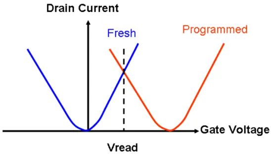
One major requirement for memory is that the threshold voltage distributions for logical states (i.e.,“1” and “0”) must be sufficiently separated to avoid read errors. The most prevailing way to determine the memory logical state is reading the current driven by the cell at a fixed gate bias. As schematically depicted in Fig. 1-6 [17], the two transfer curves which belong to the same memory cell exhibit different logical states at a fixed gate voltage, that is to say, the threshold voltage shift occurs when electron charge was stored in the FG memory. Furthermore, the threshold voltage shift is proportional to the stored electron charge. Once an acceptable amount of charge is programmed into the charge storage layer, a corresponding threshold voltage shift can effectively suppress the conduction current. Consequently, the current of the logic state “1” is very high, while the current of the logical state “0” is nearly zero, in the microampere scale.
Since conventional NOR flash memory is programmed by the channel hot electron injection (CHEI) mechanism, where electrons must gain enough energy to surmount the oxide–silicon energy barrier, thanks to the electric field in the transistor channel between source and drain. However, the high programming operation voltage will contradict the scaling criterion as a result of inducing irretrievable punch-through effect. Moreover, the concept of green transistors is increasingly important so that a novel device technology that is friendlier to gate voltage as well as drain voltage scaling down should be developed.
Recently, Schottky-barrier transistor has attracted much attention due to its high-efficiency source-side injection characteristic [24]. In this thesis, an experimental investigation was undertaken to explore the source-side injection of hot electrons at low voltage. The large gate current will realize low power CHEI programming operation for the NOR flash.
Nevertheless, Schottky-barrier transistor suffers from inherently ambipolar conduction, thus the determination of memory logical states “1” or “0” will be perturbed. Fig. 1-7 illustrates the read error case when the GIDL current is mistaken for the driving current at a fix gate voltage and thus the logical states can not be unambiguously distinguished. Accordingly, to eliminate the undesirable ambipolar conduction of Schottky-barrier devices, a novel asymmetric S/D configuration is introduced in this thesis.
A novel double patterning technique was employed to fabricate the asymmetric S/D device [25]. The adoption of n+-doped drain will facilitate the suppression of reverse drain-side hole tunneling current and thus show unipolar transfer characteristics. For memory devices, the distinctive current read is favorable for determining logical state. Fig. 1-8 illustrates the normal reading operation of memory.
1.4 Thesis Organization
There are four chapters in this thesis. Chapter 1 begins with background on Schottky-barrier MOSFETs and nonvolatile flash memory, especially the FG structure. In Chapter 2, it briefly describes the process technology related to the device fabrication and the process flow of asymmetrical (AS) SB TFT and ASSB-FG TFT memory, respectively. In Chapter 3, the basic electrical characteristics of the measured data are presented and discussed. Moreover, the preliminary programming results of ASSB-FG TFT memory are presented and analyzed. Finally, we summarize the major observations obtained in this study and give suggestions for future work in Chapter 4.
Chapter 2
Process Technology, Device Fabrication,
Measurement Setup, and Carrier
Transport Mechanisms
In this thesis, we conceive an innovative and advanced concept to realize FG memory with high programming speed and low power consumption. The fabrication of the novel asymmetric Schottky-barrier transistor involves several integrated circuits (ICs) technologies. A brief review of process technologies used in this experiment and the process flow of the proposed devices will be described in the next sections. Also, charge transport trough the tunnel dielectric is the basic mechanisms to achieve flash memory operation. We will discuss the most popular transport mechanisms of FG memory, including channel hot electron injection (CHEI), Fowler-Nordheim (FN) tunneling, and band-to-band tunneling (BTBT).2.1 Review of Asymmetric Schottky-Barrier Transistors
In the late 1980s, an asymmetric Schottky-barrier MOSFET in which the source is made up of PtSi and the drain BF2+ doped silicon was investigated by Bing-Yue
Tsui and Mao-Chieh Chen [26].The cross-sectional view of key process steps and the finished asymmetric structure is shown in Fig. 2-1 [26]. In the design of the proposed device process, the most critical step was the deionized water (DI water) rinsing step, as will be explained in the following. Briefly, after the drain-side implantation, wafers were then rinsed in DI water at 20~23℃ for 10 min. For the heavily doped poly-Si gate and drain regions, a thin native oxide layer would grow on the surface under this
rinse condition. Controlling the rinse time and water temperature carefully could induce a thin native oxide layer only on the heavily-doped gate and drain regions to hinder Pt from interacting with Si later. It should be noted that native oxide also serves as the role of gate sidewall spacer to prevent the bridging effect. In the experiment, an additional mask was used to cover the source region against drain implantation.Alignment of this mask is critical and thereby the proposed asymmetric device is difficult to scale down.
In this thesis, we propose a similar device structure having asymmetric S/D but with a more feasible process scheme. Specifically, we take advantage of a double-patterning technique recently developed by our group which employed twice I-line lithographic step to form asymmetric S/D regions [25]. Thanks to the accurate alignment, the gate length could scale down to nanoscale.
2.2 Double Patterning Technique
A double patterning lithography (DPL) technology using standard I-line lithography has been developed and proposed to shrink the gate length to 100 nm and below. The technique is capable of breaking through the resolution limit of single mask lithography using I-line stepper. DPL involves the partitioning of dense circuit patterns into two separate exposures patterning and is capable of improving the resolution and depth of focus (DOF) [27]. DPL is one of the most likely short-term solutions for keeping the pace of scaling beyond 22 nm node, since the EUV adoption timeline has been delayed [28-29]. Furthermore, DPL could be cleverly employed to fabricate asymmetric S/D device structures. In this study, a novel asymmetric SB transistor structure was designed and demonstrated successfully. To form asymmetric S/D junction, twice lithography steps with G1 mask and G2 mask were adopted as
schematically shown in Fig. 2-2 [25]. When defining the gate region, the first G1 mask covers the right part of active region in order to prevent poly-Si from dry etching and ion implantation. After doping the drain junction, the second G2 mask caps the left part of the active region and protects portion of poly-Si region remained after the previously etching. The overlapped region of the two masks thus defines the gate length.
2.3 Ni-silicide
Ni-monosilicide (NiSi) has been widely chosen and has become the most popular silicide material because of its superior properties over TiSi2 or CoSi2 for advanced
integrated circuit technology [30-32], especially 65 nm node and beyond. During the silicidation, silicon consumption of the Ni process is the smallest among Ti, Co and Ni, which facilitates the formation of ultra-shallow S/D junction [33]. Silicon consumption is defined as the distance between the initial silicon/metal interface before the siliciation and the bottom of the silicide after it is formed, as illustrated in Fig. 2-3. There is little possibility for the Ni-silicide to be formed at the sidewall since Ni is the dominant diffusion species during the formation of silicide. Therefore, bridging effect between the gate electrode and S/D hardly occurs for the NiSi due to its reaction mechanism. Moreover, NiSi has wide silisidation range of 350–750℃ and is suitable for sub-100-nm technology node. Ni reacts with Si to form Ni-rich silicide (Ni2Si) at temperatures as low as 200℃, so the NiSi is typically formed by one-step
rapid thermal annealing(RTA) at 400℃–700 ℃ for 30–60 s. The residual Ni can be selectively removed by wet etching in a mixture of H2SO4 and H2O2. Although
one-step RTA could rapidly form NiSi, excess silicide reactionwas found for short channel device and thin active region [34-35]. When Ni silicidation of the thin S/D
regions is used with excess Ni film, lateral encroachment of Ni silicide under the sidewall spacers towards the channel could occur by means of the diffusion of Ni into silicon area. In view of the possibility of excess silicide encroachment toward the channel region, moderate annealing temperature and time is crucial. To effectively control the lateral growth, in this study we adopted a one-step RTA in vacuum chamber at 500℃ for 30 seconds.
2.4 Device Structure and Process Flow
2.4.1 Process Flow of Asymmetric Schottky-Barrier TFT
(ASSB TFT) Devices
Fabrication flow of the ASSB TFT is illustrated in Figs. 2-4(a) ~ (g). Briefly, the process of all devices in this work started on 6-inch silicon wafers capped with a 250nm silicon dioxide layer. First, a 50 nm-thick undoped amorphous Si film was deposited by low pressure chemical vapor deposition (LPCVD) system at 550℃. To crystallize the amorphous Si film, the furnace annealing step was carried out at 600 ℃ for 24 hours in N2 ambient (i.e., solid-phase crystallization, SPC) [Fig. 2-4 (a)]. After
patterning active regions by a standard I-line lithography step and a subsequent anisotropic reactive plasma dry etching, a TEOS gate oxide layer was deposited by LPCVD furnace at 700℃, on which a 120 nm-thick in-situ phosphorus-doped n+ poly-Si film was then deposited [Fig. 2-4 (b)]. In this experiment, the TEOS gate dielectrics were split into three thickness conditions, i.e., 10 nm, 15nm, and 20nm, respectively. Next, the first gate photolithography of G1 mask and anisotropic dry etching step were employed to define the drain side, and then drain implantation was conducted at an energy of 12keV and dose of 5E15 cm-2 [Fig. 2-4 (c)]. The photoresist of G1 was then stripped. Subsequently, a 50 nm-thick TEOS oxide serving as hard
mask was deposited to protect the drain side from the following nickle silicidation annealing process [Fig. 2-4 (d)]. Then the second gate photolithography of G2 mask was carried out to define the real gate region. After continuously dry etching the hard mask oxide and poly-Si, the photoresist of G2 was stripped [Fig. 2-4 (e)]. Afterwards, a sidewall spacer was formed by a 20 nm-thick nitride deposition and subsequent dry etching step [Fig. 2-4 (f)]. The nitride spacers were slim so that S/D silicide reaches the gate edge due to a lateral diffusion of the NiSi under the spacers, which is crucial for the electrical performance improvement. After a diluted HF dip to remove the thin oxide layer on the source side, a 30nm-thick nickel layer was deposited immediately by physical vapor deposition (PVD) system, followed by a rapid thermal annealing (RTA) step at 500 ℃for 30 seconds for forming Ni-silicide (NiSi) metallic junction at the source region. The initial Si film at the source side is fully silicided to form NiSi which encroaches into the gate edge. A wet etching step in a mixture of H2SO4 and
H2O2 was then used to remove the unreacted metal [Fig. 2-4 (g)]. It should be noted
that no extra drain dopant activation step was necessary since the process temperature of hard mask oxide and nitride spacer was higher than 700℃ and the process time was sufficient for dopant annealing. For comparison, conventional n-type TFTs with phosphorus-doped S/D regions were fabricated using the same process conditions as described previously except that the silicide drain was replaced with ion implantation, as shown in Fig. 2-5. Finally, all devices received a standard back-end processing to completion. A post-metal annealing at 400℃ in forming gas for 30 min was performed before electrical measurements.
2.4.2 Process Flow of ASSB-Floating-Gate (FG) TFT Memory
Devices
Schematic structure of the proposed ASSB-FG TFT device is shown in Fig. 2-6. The structure and fabrication are nearly identical to those of ASSB TFT except the gate stack composition. In this configuration, a 10 nm-thick TEOS tunnel oxide and 60 nm-thick in-situ phosphorus-doped n+ poly-Si FG were deposited sequentially. Note that since the FG layer is a conductive material, the injected carriers can distribute uniformly in the storage layer. Afterwards, a 15 nm-thick TEOS oxide was deposited for the purpose of preventing charge loss from the FG charge storage layer. Then a 60 nm-thick in-situ phosphorus-doped n+ poly-Si film was deposited serving as the control gate. All deposition processes mentioned above were carried out under LPCVD system. The other process steps were identical to those described in previous sections. The control group of conventional n-type FG TFT memory was also fabricated by doping the S/D junction with phosphorus ions, as shown in Fig. 2-7.
2.5 The Measurement Setup
Electrical characteristics of the fabricated devices in this thesis are mainly characterized by automated measurement setup consisted of HP 4156 semiconductor parameter analyzer, a pulse generator Agilent-8110A, and a Visual Engineering Environment (VEE). These equipments integrated in the system are controlled by the interactive characterization software (ICS) program. In the measurement environment, the humidity is precisely regulated by dehumidifiers, while the temperature is also accurately controlled by a temperature regulated heater to maintain the measurement temperature at 25 .℃
Basic operations of program/erase that are most commonly used in actual flash memory will be reviewed, including channel hot electrons injection (CHEI), Fowler-Nordheim (FN) tunneling, band-to-band tunneling (BTBT). The three writing schemes correspond to different physical principles. It is interesting to note that the three mechanisms have been thoroughly investigated in order to avoid severe degradation results in MOSFETs. In flash memory, however, they are exploited to execute program/erase operation effectively. In the following sub-sections we will sketch these charge injection mechanisms, respectively.
2.6.1 Channel Hot Electrons Injection
The CHEI mechanism has been widely used for nonvolatile memory devices. Fig. 2-8(a) shows the mechanisms of hot-carrier injection. When the drain voltage is large enough to induce a high lateral electric field near the drain side, i.e., VD ≧ VDSAT =
VG -Vth , pinch-off occurs close to drain region and major voltage drop along the
channel occurs in the region between the pinch-off point and the drain junction. The channel electrons can gain energy far greater than the thermal-equilibrium value. Actually, the electrons energy distribution shows Maxwell-Boltzmann approximation, thus only the tail part of electrons can become sufficiently “hot” to surmount the barrier between oxide and silicon conduction band edges under a sufficiently high gate voltage, which contributes to the gate current, as illustrated in Fig. 2.8(b). Fig. 2-9 shows the electrons energy distribution [36]. Note that, the energy distribution is a function of lateral field. In the meantime, the newly generated hot electrons can ionize other atoms, leading to the so-called “impact ionization” effect. Due to the continuous collisions, a large number of electron-hole pairs can be generated. These generated secondary hot electrons can also be swept to the drain side while the holes will drift
into the substrate in an n-type transistor. In brief, two models have developed to describe the hot electron injection phenomena: the lucky electron model [37] and the energy transport model [38-40].
(1) The lucky electron model: Chenming Hu was first to use the “lucky electron” concept to empirically explore a gate current. The electrons acquire enough energy from the lateral electric field to surmount the oxide–silicon energy barrier without energy stripping collision in the channel and then be emitted into the gate oxide. In essence, the model is based on the probability that electron is lucky enough to travel several times the mean free path without scattering, eventually crossing the potential barrier. Although this simple model imposes some disagreements between theory and experimental results, it allows a straightforward and quite rough simulation of the gate current.
(2) The energy transport model: The model establishesa more rigorous theory based on a nonlocal relation between the “effective electron temperature (Te)” and the drift field. The nonlocal relationship between Te and the electric-field distribution is given by Takeda [41] as follows:
0
2
( )
(
) exp( 3 / 5
)
5
xs e sq
Te x
E x u
u
v du
k
,where q is the elementary charge, Exs is the x-component of the electric field,
k is Boltzmann's constant,v = 10s 7 cm/s is the saturated electron velocity, and
e
= 8x10-14 s is the energy relaxation time.
The heated electron gas is injected into gate dielectric. Richardson's equation in the following form can now be used to calculate gate current due to hot electrons which is dependent on electron temperature “Te”:
1/2
( )
( )[
( ) / 2
*] exp[
/
( )]
g b
Here, N(x) is minority carrier concentration,m* is the effective mass of an electron, andbis oxide barrier height.
2.6.2 Fowler-Nordheim Tunneling
In classical theory, electrons are completely confined within a potential barrier when carrier energy is lower than the potential barrier height. However, in quantum mechanics, an electron can be represented by a wavefunction, thus there is a finite probability that the charge will penetrate through the potential barrier and appear in the classical forbidden region. This phenomenon is called tunneling and it contradicts classical theory. Tunneling through the oxide can be attributed to diverse carrier injection mechanisms which depend on the oxide thickness and the applied electric field or voltage. Generally, the quantum tunneling mechanism can dominate the carrier transport when the potential barrier is sufficiently thin and it can be mainly categorized into direct tunneling (DT) and Fowler-Nordheim (FN) tunneling. FN tunneling occurs when a large electric field (Eox) is imposed on the tunneling oxide and thus electrons can tunnel through a triangular energy barrier with a width dependent on the applied bias. The FN tunneling phenomenon is given by
ox ox
q
E
t
,where q is the oxide barrier height for electrons, and t is the thickness of the ox
oxide. The energy band diagram of electrons injection from Si substrate to oxide under FN tunneling is shown in Fig. 2-10 (a). On the other hand, when the electric field built in tunneling oxide is lower than
ox
q t
, the tunneling barrier is trapezoidal as illustrated in Fig. 2-10(b) and the electrons will pass through tunneling oxide and inject into the gate directly. If the oxide is ultra thin (i.e., 3nm below), the DT
mechanism dominates over the FN tunneling. Because the reliability issue of silicon-oxide-nitride-oxide-silicon (SONOS) memory is ascribed to the leakage due to DT, the tunneling oxide thickness can not scale below 3nm.
2.6.3 Band-to-Band Tunneling
When a highly negative voltage relative to n+drain region is applied to the gate, a deep depletion region occurs underneath the gate-to-drain overlap region. Because of the serious band bending in the deep depletion region induced by a large electric field, electrons may tunnel directly from valance band through a potential barrier into conduction band. Simultaneously, the majority of the holes flow into the substrate due to the lateral field and are observed as the substrate current in bulk MOSFETs. In the course of BTBT, electron-hole pairs are generated and they are “cold” [42]. A part of the created holes will acquire enough energy from the lateral electric field without suffering any collision to surmount the Si-SiO2 energy barrier, thus contributing to the
gate leakage current. Note that in this special case, the potential barrier has a triangular shape with the maximum height given by the energy gap. This tunneling process is schematically shown in Fig. 2-11.
2.6.4 Summary
For conventional NOR flash memory, programming is performed by CHEI near the drain side. However, the drain-side hot electrons suffer from the conflict between favorable vertical oxide field and maximum lateral drain field, thus the injection efficiency is very low in highly scaled devices. In order to solve the lower program-efficiency problem, source-side-injection (SSI) scheme was developed for high-speed and low-voltage operation. A FG memory device with high programming
Chapter 3
Results and Discussion
3.1 Fundamental Electrical Characteristics
Devices of asymmetric S/D configuration can be operated in two different modes, that is to say, forward and reversed modes, respectively. For the forward mode, the Ni-silicided junction is used as the source while the n+-doped junction is used as the drain. On the contrary, the reverse mode measurements were carried out by interchanging the source and drain terminals. Fig. 3-1 illustrates the bias configurations of the ASSB-TFT under forward and reverse operation modes. The experimental transfer characteristics of n-type asymmetric Ni-silicided SB-TFTs are
discussed in the following paragraphs.
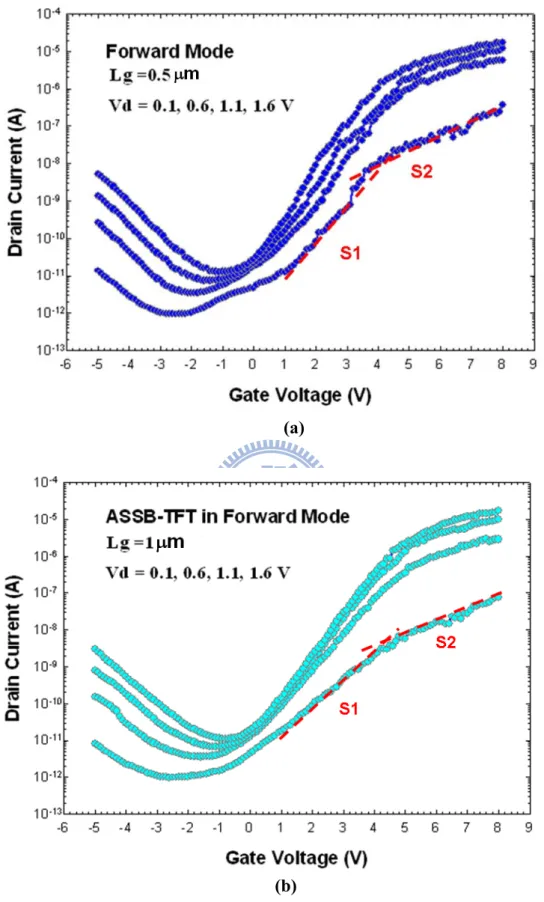
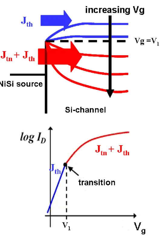
Figs. 3-2 (a) and (b) show the transfer characteristics of n-type ASSB-TFT devices operated under forward mode with nominal channel length of 0.5 μm and 1 μm, respectively. The drain voltage varies from 0.1V to 1.6V with 0.5V voltage steps. It is obvious that both devices exhibit a two-step subthreshold swing (SS) (dashed line in Fig. 3-2) with increasingly positive gate voltage (Vg), a feature significantly different from that of conventional MOSFETs, i.e., doped S/D-junctions devices. Such a phenomenon originates from the competition of two different carrier injection mechanisms, thermionic emission current (Jth) and tunneling current (Jtn) [43], which are conceptually illustrated with the band diagrams shown in Fig. 3-3. As can be seen in the figure, in the subthreshold regions, as the applied Vg is low, thermionic emission current (Jth) dominates the conduction, so only carriers with energy greater than the Schottky barrier height (SBH) contribute to the current, as schematically
displayed in blue in the figure. When Vg is increased to the level Vg = V1, the band of
the channel near the source junction becomes flat (dashed line in Fig. 3-3). When Vg further increases over V1, the current now consists of both the Jth and the Jtn components, represented by the red lines in Fig. 3.3. With a sufficiently high Vg, tunneling current dominates the current flow as the Schottky barrier is thinned.
In brief, when the potential barrier is higher than the SBH at the source side, the thermionic current dominates and thus the SS is nearly a constant. However, when the device is turned on, the main increase in current arises from the tunneling through the SB at the source and is strongly dependent on the shape of the SB which is modulated by Vg. The tunneling current is a function of the SBH between the metal and the semiconductor, the gate dielectric thickness and gate voltage.Fig. 3-4 shows transfer characteristics of devices operated under the forward mode with different gate oxide thicknesses. It can be seen that, with the increase in oxide thickness, the drain current is lowered and thus degrades the device performance. On the other hand, the reduction of gate oxide thickness causes an increase of the electric field under the gate which makes the cell transistor more susceptible to gate-induced drain leakage (GIDL). The GIDL current is the tunneling mechanism caused by band-to-band tunneling or trap-assisted tunneling in the gate-to-drain overlap region and can dominate the drain leakage current even at zero gate bias in field-effect transistors (FET) with ultra-thin gate oxide [44].
Fig.3-5 shows and compares the transfer characteristics of an ASSB-TFT operated in forward and reverse modes, respectively, together with a conventional n-type impurity-doped TFT device with the same channel length/width and gate oxide thickness. It is obvious that the n-type ASSB-TFT in forward mode depicts improved
μA/μm (normalized to the channel width of 10 μm), where ION is chosen as the
maximal ID and IOFF is the minimal one. The lowered off-current is ascribed to the
prohibition of hole tunneling current from the n+-doped drain side. Conversely, under reverse operation mode, an undesirable off-state current is ascribed to hole tunneling from the silicided-drain junction, resulting in a deteriorated ION/IOFF of around 104.
Note that, it is apparently that the ASSB-TFT operated in forward mode suffers from lower on-current, and a poorer SS. The degraded driving capability is ascribed to the high source resistance due to the high Schottky barrier at the silicon/silicide source junction. The presence of NiSi/Si SB junction offers a potential barrier for electrons of about 0.65 eV [45]. The tunneling distance is spatially modulated by the gate voltage and conduction occurs when the tunneling distance is sufficiently small.
Although conventional SB transistors have several advantages, as was described in Chapter 1, the drawback of abnormally high drain leakage current attributed to the GIDL-like effect is a serious problem, especially for memory application. Several studies have reported that ambipolar conduction could cause misidentification of memory logical states [45-49]. Utilization of an asymmetric S/D structure to eliminate off-state leakage and achieve unipolar conduction has been introduced in previous chapters. Figs. 3-6 and 3-7 depict the energy band diagrams of conventional symmetric Schottky-barrier transistors and the ASSB-TFT devices, respectively, operated at various bias conditions. The band diagrams for ASSB structure and conventional SB devices are quite similar except at the drain region where the metal silicide of the symmetrical structure is replaced by the heavily-doped silicon in ASSB structure. Compared with the conventional Schottky-barrier transistors, the ASSB-TFT structures can significantly suppress the gate-induced drain leakage (GIDL)-like off-current and thus mitigate the undesirable ambipolar conduction of conventional SB devices.
Due to the fact that NiSi is a mid-gap material, SB devices with NiSi serving as S/D could be operated in either n- or p-channel, depending on the gate and drain bias polarity. In this study, we have also fabricated p-type ASSB-TFT devices, namely, the P+-doped junction was replaced with BF2+ doped junction schematically shown in Fig.
3-8. The definitions of operation modes are the same as those mentioned above. The transfer characteristics of a p-type ASSB-TFT device operated under forward mode and reverse mode are shown in Fig. 3-9. For the forward mode, the GIDL-like leakage current is suppressed by one order of magnitude as compared with that of the reverse mode, although its on-current is also degraded.
Fig. 3-10 shows the transfer characteristics in forward mode for both n- and p-channel operations under proper bias conditions. For n-channel operation, field emission of electrons from the source junction contributes to the on-state current. On the other hand, when the device is operated at p-channel mode, the on-state current is ascribed to the field emission of holes from the source junction. It is interesting to note that both channel operations exhibit comparable drive capability.Although the barrier height of the NiSi/silicon Schottky junction for holes (~ 0.45eV) is less than that for electrons (~ 0.65 eV), the effective mass of holes for Schottky tunneling is higher than that of electrons. Thus, a comparable on-state current is reasonable.
3.2 Source-side Hot Electron Injection
In this section, we report on the experimental evidence of hot-electron injection at the Schottky source side. Fig. 3-11 shows gate current (Ig) versus drain voltage (Vd) characteristics as a function of gate voltage (Vg) operated in forward mode. A striking gate current can be attained when Vg is higher than 6V and Vd is higher than 3V. With the increase in Vg, Ig also increases significantly. The significant gate current is
mainly associated with the unique Schottky barrier at the source/channel interface,
which could induce an abrupt band bending and a high lateral electric field near the source region. Compared with the conventional transistors with impurity-doped S/D junctions, most of the voltage drop along the surface channel occurs at the region near the source side rather than the drain side. Fig. 3-12 schematically illustrates the energy band diagrams of both the ASSB-TFT device under forward mode and the conventional device under a bias condition that hot electron injection would occur, respectively. The strong field is located at the source-side region in the source-side Schottky-barrier cell, whereas it is located at the drain-side region in the conventional device. At sufficiently high Vg and Vd, electrons can become so energetic that they can conquer oxide barrier height (~ 3.1 eV) and then be trapped in the oxide. On the contrary, if the drain bias is insufficient, electrons could not acquire enough energy to surmount the electric barrier of the oxide and thus no pronounced Ig is observed. Note that, the gate dielectric used in this experiment is LPCVD TEOS oxide, so the electron trapping is a transient behavior that is called “dynamic electron trapping” [49]. At the bias conditions as same as those used in Fig. 3-11, the output characteristics of the ASSB TFT in forward mode are shown in Fig. 3-13. When the bias condition is conducive to the source-side hot electron injection, the Id-Vd curves show a characteristic negative-differential-conductance (NDC) behavior, that is, the drain current decreases with increasing drain voltage. It should be noted that the magnitude of the drain current is not consistent with that of the gate current, implying that the gate current is not the direct origin of the drain current decrease. Rather, the NDC behavior is ascribed to an upward Vth shift due to dynamic electron trapping, and thus the conduction current is decreased. Fig. 3-14 shows the plot of the subthreshold characteristics of a device before and after the dynamic electron trapping. Significant shift in Vth is in agreement with the behavior of source-side hot electron
injection as well as the NDC effect.
Fig. 3-15 and Fig. 3-16 show the Ig versus Vd characteristics for reverse mode case and conventional device, respectively, in which the source is made of a phosphorous-doped Si. Compared with the forward operation mode, no pronounced gate current is seen due to the insufficient lateral electric field along the channel. Fig. 3-17 compares the output characteristics of the ASSB-TFT in reverse mode and the conventional device. Due to the absence of striking gate current, the NDC behavior is not observed. In Fig. 3-17, the devices have channel length of 1 μm. It is clearly indicated that the magnitude of Id in both devices is at the similar level except for a finite drain voltage offset of around 0.5V (dashed circle in Fig. 3-17) for the ASSB device. Furthermore, the sublinear characteristic of ASSB-TFT operated in reverse mode is obviously shown in the linear region. The above results clearly indicate that the peculiar behavior deviations from the conventional devices can be ascribed to the Schottky barrier formed between NiSi drain side and Si channel. The built-in potential barrier associated with this NiSi drain continues to impede current flow at higher drain biases. Fig. 3-18 presents the output characteristics of an ASSB-TFT operated in reverse mod with channel length of 5 μm. In the long-channel device, these characteristics are well saturated and no sublinear behavior is observed in the linear regime when drain biases are larger than gate biases, i.e., Vd > Vg. The saturation current at the gate voltage of 6 V is 15μA/μm.
Although the pronounced source-side hot electron current has successfully been demonstrated at the bias condition of Vg higher than 6V and Vd higher than 3V, a striking leakage is also found when Vg is sufficiently large and Vd is nearly 0V during the device characterization shown in Fig. 3-11. The gate current starts at a Vd much less than that demanded for generation of hot electrons, indicating that Fowler-Nordheim (FN) tunneling is likely to be responsible for the gate leakage. This
phenomenon suggests that a fraction of channel electrons could tunnel through the gate oxide into gate electrode, implying the Vth shifts are mainly attributed to both FN tunneling current and source-side hot electrons injection. Theoretically, the transport mechanism of FN tunneling features a uniform channel injection, which is highly dependent on channel length. Conversely, the source-dide hot electron injection through the gate oxide, localized around the source side, has little dependence on the channel length. Figs. 3-19 (a) and (b) depict and compare the injection location of source-side hot electron injection and FN tunneling, respectively. Next, to further verify that the unexpected occurrence of gate current around Vd =0V is indeed due to FN-tunneling, we examine the dependence between the magnitude of gate current and the gate length. Figs.3-20 (a) ~ (e) show Ig versus drain Vd characteristics with channel lengths of 0.5μm, 1μm, 2μm, 5μm, and 10μm, respectively. Drain voltage is varied from 0 to 6 V and the gate voltage from 3 to 9V with 1 V/step. The channel width in these characterized devices is 10 μm. Based on the experimental results, the gate current characteristics are observed and analyzed by the following two viewpoints.
In the figures for each individual device biased at lower drain biases, especially Vd <1V, the FN-tunneling gate current is prevailing, and the gate current is a function of gate voltage. At higher drain biases, the FN- tunneling effect is weakened, and thus the magnitude of gate current is lowered until hot electron injection current becomes significant. When the drain bias further increases (Vd > 3V), a high lateral electric field is developed at the silicided source junction and triggers the generation of hot electrons and subsequent injection into the channel. Under a sufficient gate bias, hot electrons would be injected into gate oxide at a location around the source. Briefly, the gate current has three main regimes when the drain bias varies during electrical characterization. Second, we compare the magnitude of gate current with different
channel lengths. As the channel length increases, the FN-tunneling is more dominant
due to the increase of injection area. On the other hand, the magnitude of gate current in the hot electrons injection regime is independent of channel lengths, that is, the peak value of gate current at a fixed Vg is kept nearly constant regardless of the channel length. Contrary to FN tunneling, the hot electrons injection through the gate oxide, localized around source side, has little dependence on length.
It should be noted that both FN tunneling and source-side hot electron injection depend on gate voltage and oxide thickness. Figs. 3-21 (a) ~ (d) show Ig versus drain Vd characteristics with various channel lengths at Vg of 5V, 6V, 7V, and 8V, respectively. When Vg is smaller than or at 5V, the ASSB-TFT devices do not show
any prominent gate current, as shown in Fig. 3-21 (a). When the gate bias is 6V and the drain bias is higher than 3V, the injection of source-side hot electron is provoked. As shown in Fig. 3-21 (b), it also clearly indicates that the magnitude of hot electron current is constant regardless of the channel length. If Vg is more than 7V, FN tunneling current occurs at low drain bias regime with a level which would surpass the hot electron injection current, especially for long-channel devices, as shown in Figs. 3-21 (c) and (d).
Due to the strong dependence on injection area and vertical electrical field across the gate oxide, it is supposed that FN-tunneling current is in direct proportion to the channel length. Hence, we extract the values of gate current at Vd = 0V, in which FN tunneling is throughout the channel because both source and drain are grounded while a highly positive bias is applied to the gate to induce strong electric field. All characterized devices have gate oxide thickness of 10 nm and channel width of 10 μm. Fig.3-22 displays the nearly linear dependence between FN-tunneling current and channel lengths. Moreover, when gate voltage is higher than 8V, the FN tunneling is dramatically raised.
thickness of 10nm and 15 nm, respectively. At the same bias condition (Vg=8V), it can be shown that the Ig is largely suppressed when the oxide thickness is increased to 15nm. The source-side region experiences a vertical field which depends on the thickness of gate stack composition and the applied voltage. Consequently, in order to improve the injection efficiency, the thickness of oxide layers should be optimized.
Unlike the inherent source-side band bending of ASSB devices operated in forward mode, the major voltage drop for devices with heavily-doped source junction occurs near the drain side, where electrons can attain energy to surmount oxide barrier. However, the drain-side region has a relatively low vertical electric field due to the low gate-to-drain potential difference (i.e., Vg-Vd). As a result, the injection efficiency is not ideal. As a result, both high gate and drain voltages are required to ensure sufficient injection efficiency. Fig. 3-24 shows the comparison of gate current operated in two modes for an ASSB device together with its conventional control device. It is apparent that the ASSB device using NiSi layer as the source exhibits the best injection efficiency of hot electron current.
3.3 Program Characteristics of ASSB-FG Memory
Based on previous observations, we propose a novel ASSB-FG memory and explore the effect of source-side injection for programming applications. As mentioned in previous sections, the long-channel devices, especially for the device with channel length of 10 μm, suffer from the effect of FN tunneling which obviously outperforms the hot-electron injection at Vg more than 8V. As a result, we will prefer short-channel devices to carry out memory programming test in order to understand the effect of hot carrier injection mechanism more clearly. Here, devices with channel length of 0.6 μm were utilized in this study. All FG memory devices which are
discussed in this section have oxide thickness of 10 nm. For ASSB-FG memory, we carry outprogramming operation under forward mode.
Fig. 3-25 shows the transfer characteristics of the ASSB-FG device before and after programming operation with Vg=12V, Vd=6V for 100 μs. It indicates that subthreshold swing of the programmed device is almost identical to that of the fresh state. Therefore, we can fairly use the constant current method to determine the Vth. Here, owing to the poor subthreshold swing, the value of Vth is defined as the gate voltage (Vg) to achieve a drain current Id = 1nA.
Fig. 3-26 depicts the Vth shift versus programming time of the ASSB-FG memory device at Vg = 8V and various drain voltages. It can be found that when Vd is more than 6V, an acceptable programming speed could be achieved. This is because a high Vd is necessary to induce a high lateral electric field for the generation of hot electrons and a high Vg is indispensable for attaining a sufficient vertical electric field for the injection of hot electrons into the FG storage node.
Figs. 3-27 (a) and (b) plot the programming speed of ASSB-FG and conventional FG devices at various bias conditions, respectively. The programming conditions of Vg = 12V and Vd = 6V with programming time of 10 ms exhibit a threshold voltage (Vth) shift of around 6 V in the ASSB-FG device. On the contrary, in the conventional
n-type counterpart cells, the drain-side hot electrons suffer from the conflict between gate-controlled and lateral drain fields. Therefore, in the same bias conditions, especially Vg smaller than 10V, the conventional TFT FG memory devices exhibit hardly any Vth shift. This main difference between the two devices is attributed to the existence of high lateral and vertical electric field at the source side, which would originate from the sharp band bending caused by the innate band profile. Most importantly, the absence of conflict between Vd and Vg for the source-side injection memory can promise a high-speed programming at low voltage conditions.
It is worthy to note that, we have demonstrated the novel FG memory devices on poly-Si channel in this study. Generally, the potential barrier stemmed from the grain boundaries of poly-Si channel would hinder the electrons from acquiring sufficient energy to cause impact ionization in the channel transport from source to drain, thus defeating the purpose of programming memory devices. In contrast to a conventional TFT device, however, the ASSB TFT FG memory naturally has an abrupt band bending characteristic near the source-side region, which enables charge carrier to become “hot” enough, even as the applied gate and drain voltages are low.
3.4 Discussion
Although we have successfully fabricated ASSB-FG memory devices with a satisfactory programming speed, the poor subthreshold swing may be an issue of reliability. The poor subthreshold swing seems to arise from an un-gated region between the silicided source and the polysilicon channel, due to a faulty process control of NiSi formation. To make it clear, in Fig. 3-28, the cross-sectional transmission electron microscopic (TEM) image of a fabricated ASSB-FG device is shown. In an ideal case, the gate electrode should moderately overlap the source barrier. However, an offset region (as indicated by the double-headed arrow in Fig. 3-28) is clearly seen between the NiSi Schottky-barrier source and the channel, leading to an increase in the parasitic resistance from source to channel in the ASSB devices. As a consequence, the conduction electrons have to transport across the un-gated region and the carrier tunneling current is severely limited, resulting in the degraded subthreshold swing. Briefly, this unwanted offset region could be ascribed to a non-optimum fabrication process and an insufficient over etching, leading to oxide
![Fig. 2-1 The cross-sectional view of the rinsed asymmetric Schottky barrier PMOS process sequence and the finished structure [26]](https://thumb-ap.123doks.com/thumbv2/9libinfo/8755748.206860/59.892.222.689.112.747/sectional-asymmetric-schottky-barrier-process-sequence-finished-structure.webp)