國 立 交 通 大 學
顯示科技研究所
碩士論文
非晶矽 / 微晶矽 疊層薄膜太陽能電池之
模擬與微晶矽結晶率之探討
Tandem a-Si:H / μc-Si:H Thin Film Solar Cells:
Modeling & Control of Crystallinity of μc-Si:H
研究生:曾威豪 Wei-Hao Tseng
指導教授:蔡娟娟 教授 Prof. C.C Tsai
中華民國九十八年 八月
非晶矽 / 微晶矽 疊層薄膜太陽能電池之
模擬與微晶矽結晶率之探討
Tandem a-Si:H / μc-Si:H Thin Film Solar Cells:
Modeling & Control of Crystallinity of μc-Si:H
研究生 : 曾威豪 Student: Wei-hao Tseng
指導教授 : 蔡娟娟 教授 Advisor: Prof. C.C. Tsai
國立交通大學
顯示科技研究所
碩士論文
A thesis
Submitted to Department of Photonics Display Institute
College of Electrical Engineering and Computer Science National Chiao Tung University
In partial Fulfillment of the Requirements For the Degree of
Master In
Electro-Optical Engineering August 2009
Hsinchu, Taiwan, Republic of China 中華民國九十八年八月
中文摘要
在本論文中,我們以 Atlas 軟體建立新型矽基薄膜太陽電池模擬模組,並討論各種 物理參數對於元件效率的影響。單接面的氫化非晶矽和氫化微晶矽太陽能電池皆以 Atlas 模擬出其電學特性,之後再將非晶矽和微晶矽電池疊層構成的雙接面太陽能電池進行模 擬。當改變底層太陽能電池吸收層的能隙以及電子能態中帶尾能態的分佈時,開路電壓 (Voc) 會隨著能隙增加而上升,短路電流 (Jsc) 則是在能隙小於 1.4 電子伏特後,開始下 降。這是因為電子和電洞佔據在侷限能態 (localized state) 上是無法有效移動,造成短路 電流 (Jsc) 的下降。除此之外,我們也利用射頻電漿輔助化學氣相沉積系統 (PECVD) 製 作氫化微晶矽薄膜。對於氫化微晶矽薄膜太陽能電池而言,結晶率是相當重要的議題。 實驗中以利用調變氫氣流量,電漿能量還有不同的基板進行對於控制結晶率的研究。Abstract
In this study, a detailed electrical-optical computer modeling, based on the Atlas software, was used to investigate the effect of bandgap (Eg) and tail state distribution of intrinsic
microcrystalline silicon thin film on thin film silicon solar cells. Complete tandem solar cell which consists of an a-Si:H top cell and a μc-Si:H bottom cell solar cell were simulated. In this study the bandgap and tail state distribution of the bottom cell were varied. The acceptor and donor tail state distribution of i-layer was assumed to be broader as the Eg increases in the
bottom cells. WTA and WTD are used to represent the characteristic energy for acceptor-like tail state distribution, and characteristic energy for the donor-like tail state distribution, respectively.The open circuit voltage (Voc) increased with increasing Eg, but the short circuit
current (Jsc) decreases when Eg is lower than 1.4eV. The lower Eg made the Voc and efficiency
decease sharply, although the Jsc was kept at high value. Comparing the highest (1.6 eV) and
lowest Eg (1.1 eV), the former has a better performance. Therefore, the Eg of bottom cell
should not be lower than 1.3eV to avoid the decline of efficiency.
In the second part of this thesis, I have studied the control of crystallinity in the growth
of μc-Si:H thin films during plasma-enhanced chemical vapor deposition (PECVD) process. The crystallinity of μc-Si:H film increases with increasing film thickness. Through modulating the H2 flow in the deposition process, the crystallinity could be controlled. Base
on the experimental results, the initial deposition condition is crucial for further growth. Through altering the deposition conditions and modulating the hydrogen flow, uniform crystallinity of about 50% could be achieved.
誌謝
兩年以來,從一個完全不懂太陽電池的學生到現在順利完成論文,真的要感謝許多 曾幫過我的人,首先必須要感謝顯示所的冉曉雯副教授,在實驗研究部份因為有老師的 細心指導還有在旁的協助,才能使我的研究能得以順利進行,在此特別感謝老師的栽培 以及付出。接下來我的指導教授蔡娟娟老師,她教導我許多做人處事方法以及研究學問 的態度,在這兩年研究生涯的敦敦教誨之下使我受益匪淺。在科學研究方面的嚴謹態 度,在社會上做事的方式,使得學生在兩年碩士生涯學習甚多,特此感謝老師的指導。 還要感謝綠色能源研究中心在實驗上給我的各種幫忙,口試委員冉曉雯老師、吳耀 銓老師、劉柏村老師於百忙之中撥冗前來,提供我許多寶貴意見,使得本論文更臻於完 善。此外,交通大學奈米中心的林聖欽先生、倪月珍小姐、黃國華先生、何惟梅小姐、 崔秉鉞主任、優貝克的陳江耀、張文心、張智浩及Morris在裝機時以及實驗上的指導還 有Silvaco的范萬達,各位在這裡給我的各種幫忙,內心亦不勝感激。 感謝博後光電所博士班顏國錫學長、黃 彥 棠學長、徐振航學長、光電所王建敏同 學、顯示所姚芳弘、陳達欣同學,同學之間的互相勉勵以及另外一組的黃慶能、袁煥之 大家感情融洽,常常忙裡偷閒,使得兩年的碩士生涯充滿了回憶,還有許翼鵬、許宏榮、 李建亞、鄭柏翔學弟以及另一組的琇文學妹和世益學弟大家給予我的實在太多太多,除 了協助實驗之外並在我最艱苦的時候陪我渡過最後的關頭,所有在本實驗室的碩一學弟 妹,看到你們所製作的卡片,真的讓我很感動,謝謝大家,在此獻上我最誠摰的祝福與 II
謝意。最後,要深深感謝我最愛的家人,陪我度過許多挫折及分享我的喜悅,並在精神 上永遠支持我,沒有你們在背後的支持就沒有現在的我,在此,願將這份榮耀與你們一 同分享。
Contents
中文摘要 ... I ABSTRACT ... I 誌謝 ... II FIGURE CAPTIONS...………….………...Ⅵ TABLE CAPTIONS...………….………...Ⅸ CHAPTER 1 INTRODUCTION ... 11.1 CURRENT PROGRESS OF SOLAR CELL TECHNOLOGIES ... 1
1.2 SILICON THIN FILM SOLAR CELL ... 2
1.3 SILVACO DEVICE SIMULATOR ... 4
1.4 MOTIVATION ... 6
CHAPTER 2 LITERATURE REVIEW ... 7
2.1 SILICON THIN FILM SOLAR CELL ... 7
2.1.1 Single-Junction Amorphous Si Solar Cells ... 7
2.1.2 Single-Junction Microcrystalline Si Solar Cells ... 12
2.1.3 Tandem Solar Cell ... 15
2.2 DEPOSITION MECHANISMS OF µC-SI:HTHIN FILM ... 17
2.2.1 Surface Diffusion Model ... 17
2.2.2 Selective Etching Model ... 18
2.2.3 Chemical Annealing Model ... 20
CHAPTER 3 EXPERIMENTAL TECHNIQUE ... 22
3.1 PLASMA-ENHANCED CHEMICAL VAPOR DEPOSITION ... 22
3.2 RAMAN SPECTRUM ... 22
CHAPTER 4 RESULTS AND DISCUSSIONS ... 24
4.1 HYDROGENATED AMORPHOUS SI SOLAR CELL ... 24
4.1.1 Simulation Model ... 24
4.2 MICROCRYSTALLINE SI SOLAR CELL ... 30
4.2.1 Simulation Model ... 31
4.3 TANDEM SOLAR CELL WITH AND WITHOUT X LAYER... 35
4.3.1 Simulation Model ... 36
4.4 THE EFFECT OF THE BANDGAP IN BOTTOM CELL ON THE SOLAR CELL PERFORMANCE ... 42
4.4.1 Influence of i-Layer Bandgap on Single-Junction Cell Performance ... 42
4.4.2 Influence of Bottom Cell Bandgap on Tandem Cell Performance ... 44
4.5 DEPOSITION TECHNIQUES FOR MICROCRYSTALLINE SILICON ... 46
4.5.1 Effect of H2 Dilution on Crystallinity ... 46
4.5.2 Effect of rf Power on Crystallinity ... 47
4.5.3 Effect of Total Gas Flow ... 47
4.5.4 Crystallinity vs. modulating the H2 flow percentage of next layer ... 49
4.5.5 Crystallinity vs. modulating the initial H2 flow ... 50
4.5.6 Effect of varied SiH4 flow rate of three substrateson crystallinity of µc-Si:H film ... 51
CHAPTER 5 CONCLUSIONS ... 53
REFERENCE ... 55
Figure Captions
Chapter 1
Fig. 1-1 Panel of the different PV technologies with their conversion efficiencies, from high performance multi-junction GaInP/GaAs/Ge to very low cost chemical dye sensitized cells [13].
Fig. 1-2 Silicon atomic structure of (a) crystalline silicon (b) hydrogenated amorphous silicon.
Chapter 2
Fig. 2-1 The dark conductivity σ, activation energy Eσ, and estimated position of Fermi level EF for a-Si:H, as a function of gas phase doping ratio NPH3/NSiH4 (for n-type layers) and NB2H6/NSiH4 (for p-type layers). Eσ* is the estimated ‘true’ distance between band edge (Ec, Ev) and the Fermi level EF, where the statistical shift Es has also been taken into consideration for n-type layers, assuming a constant defect density of 1016 /cm2 eV. For p-type layers, an identical correction Es has been assumed. In the graph, the equivalent bandgap of a-Si:H, or the ‘mobility gap’, istaken to be 1.7 eV.
Fig. 2-2 Density of states of a-Si:H [4].
Fig. 2-3 Defect-related optical absorption in as-deposited and degraded state for a series of single-junction µc-Si:H silicon p-i-n solar cells as a function of the crystallinity of the intrinsic layer (i-layer) [8].
Fig. 2-4 The optical absorption coefficient α and the penetration depth dλ, where dλ = 1/α of monochromatic light with photon energy hυ and wavelength λ, for crystalline silicon (c-Si), and typical device-quality a-Si:H and µc-Si:H layers
on glass. The curve for µc-Si:H has been corrected for light scattering due to
surface roughness [10].
Fig. 2-5 Schematic representation of the surface diffusion model. The hydrogen atoms from the plasma passivate all the surface dangling bonds, hence enhancing the surface diffusion length of silicon radicals, which have to find an adequate site to attach [15].
Fig. 2-6 Schematic representation of the selective etching model. The hydrogen atoms from the plasma etch preferentially the amorphous silicon phase, favoring the growth of the crystalline phase, resulting in µc-Si:H [15].
Fig. 2-7 Schematic representation of the chemical annealing model. The hydrogen atoms from the plasma recombine with hydrogen bonded to surface or sub-surface silicon atoms, delivering vibrational energy which favors silicon crystallization [15].
Chapter 3
Fig. 3-1 Micro-Raman spectrometer composed of an He-Ne laser source, a microscope, a notch filter, a grating and a CCD camera [20].
Chapter 4
Fig. 4-1 Schematics of an a-Si solar cell structure, which consists of glass/ITO/a-Si:H p-i-n/Ag.
Fig. 4-2 Distribution of acceptor/donor-like trap states across the forbidden energy gap used in i-layer in the simulation.
Fig. 4-3 The illuminated J-V characteristic curve of a-Si:H p-i-n solar cell.
Fig. 4-4 Photovoltaic performance of a-Si:H solar cell with different Ndb of i layer. Fig. 4-5 The J-V characteristics curve with different Ndb in i layer of a-Si:H cells.
Fig. 4-6 μc-Si:H solar cell structure, which comprises glass/ITO/μc-Si:H p-i/a-Si:H n/Ag
Fig. 4-7 Distribution of acceptor/donor-like trap states across the forbidden energy gap used in i-layer in the simulation study.
Fig. 4-8 The illuminated J-V characteristic curve of μc-Si:H p-i-n solar cell. Fig. 4-9 Tandem solar cell without x layer.
Fig. 4-10 Tandem solar cell with x layer.
Fig. 4-11 The J-V curves of tandem solar cells with and without x layer.
Fig. 4-12 The added-x layer TRJ (tunneling recombination junction) band diagram. The strategy is to simulate the tunneling effect around x region in band gap. Fig. 4-13 Change transport in tandem cells under AM1.5G illumination conditions.
(a) Hole current density distribution; (b) Electron current density distribution; (c) Recombination rate distribution.
Fig. 4-14 Photovoltaic performances of single-junction cells with different Eg of i layers Fig. 4-15 The J-V curves of single-junction cells with varied Eg of i-layers.
Fig. 4-16 Photovoltaic performances of tandem solar cell with varied Eg of bottom cell. Fig. 4-17 The J-V curves of tandem solar cells with varied Eg of bottom cell.
Fig. 4-18 The crystallinity of µc-Si:H increases with H2 flow. Fig. 4-19 The crystallinity of µc-Si:H increases with rf Power Fig. 4-20 Deposition rate vs. relative total gas flow (F / F0). Fig. 4-21 Crystallinity vs. relative total gas flow (F / F0) Fig. 4-22 Crystallinity vs. next layer H2 flow percentage Z Fig. 4-23 Crystallinity vs. initial H2 flow F0
Fig. 4-24 The deposited parameters of µc-Si:H film.
Fig. 4-25 Crystallinity with different SiH4 flow rate on three different substrates.
IX
Table Captions
Chapter 4
Table 4-1 Device Parameters of a-Si:H solar cell used in Simulations. Table 4-2 Device Parameters of μc-Si:H solar cell used in Simulations. Table 4-3 The electrical characteristics for a-Si:H and μc-Si:H solar cells. Table 4-4 TRJ (a-Si:H n-layer, x layer, µc-Si:H p-layer) parameters.
Table 4-5 Simulation results for µc-Si:H solar cell with different Eg of i layers. Table 4-6 Simulation results for tandem solar cell with varied Eg of bottom cell.
Chapter 1
Introduction
1.1 Current Progress of Solar Cell Technologies
The constant energy consumption and expansion of population add to the potential risks of ecological and human disaster associated with global warming. This makes the energy crisis will be the top issue affecting the humanity 50 years from now. It is necessary to develop renewable energy technologies such as photovoltaic energy. These technologies already exist, however, the cost disadvantage of the PV is still significant compared to fossil-based and nuclear energies, despite of the variety of PV technologies. There are many different types of PV design using different type of materials or structures as shown in Fig. . For the common crystalline and multi-crystalline silicon cells which have high conversion efficiencies, there are the III-V and the chalcopyrite based solar cells composed of more exotic compounds (As, Sb, Ga, In,...) which have also high conversion efficiencies. But these technologies cause serious contamination for global environment because of the toxicity of their constituents. All these types of cells can be combined into multi-junction cells which present very high conversion efficiencies of up to 30 %. The main disadvantage of these cells is that they are all deposited on crystalline silicon wafers making them economically and environmentally expensive. On the other hand, chemical dye sensitized cells are very cheap, but show poor conversion efficiency of about 5 - 7 % [1] so far.
Fig. 1-1 Panel of the different PV technologies with their conversion efficiencies, from high performance multi-junction GaInP/GaAs/Ge to very low cost chemical dye sensitized cells [13].
1.2 Silicon Thin Film Solar Cell
The silicon thin film does not come from expensive monocrystalline ingots but is grown by chemical vapor deposition (CVD) on inexpensive substrates such as glass, stainless steel or plastic. The deposited silicon can present as either an amorphous (a-Si:H) or a microcrystalline (µc-Si:H) structure and the resulting PV solar cells with conversion efficiency of about 10% can be achieved [13].
Hydrogenated amorphous silicon (a-Si:H) is the non-crystalline allotropic form of silicon. It can be deposited in thin films at low temperatures onto a variety of substrates. Silicon is a four-fold coordinated atom that is normally tetrahedrally bonded to four neighboring silicon atoms. In crystalline silicon this tetrahedral structure is continued over a large range, forming a well-ordered lattice (crystalline), as shown in Fig. 1-2(a). In amorphous silicon this long
range order is not present and the atoms form a continuous random network, as shown in Fig.
1-2(b). Not all the atoms within amorphous silicon are four-fold coordinated. Due to the
disordered nature of the material some atoms have a dangling bond. These dangling bonds are defects in the silicon random network, which cause anomalous electrical behavior. If desired, the material can be passivated by hydrogen, which bonds to the dangling bonds and can reduce the dangling bond density by several orders of magnitude. In general, there exist about 10 at% hydrogen concentrations in hydrogenated amorphous silicon thin film. Hydrogenated amorphous silicon has a sufficiently low amount of defects to be used within devices. However, the hydrogen is unfortunately associated with light induced degradation of the material, termed the Staebler-Wronski effect.
Fig. 1-2 Silicon atomic structure of (a) crystalline silicon (b) hydrogenated amorphous silicon.
Microcrystalline and amorphous silicon layers have quiet different material properties: (1) It is a complex material microstructure that made by drastic deposition conditions. (2) It is sensitivity to layer contamination.
(3) The bandgap of µc-Si:H is lower than a-Si:H (1.7 to 1.8 eV for a-Si:H). Due to this, the incoming light in the near infrared region of the solar spectrum can be absorbed.
(4) An indirect bandgap, it means a lower absorption coefficient in the visible range of the solar spectrum compared with a-Si:H. Therefore it is necessary for using thicker
absorbing layers than in the case of a-Si:H and more efficient light trapping within the solar cell.
(5) The most important thing is a much milder from the light induced degradation.
The best single junction microcrystalline silicon solar cells have 9 to 10 % range efficiency. Now the best way of using the microcrystalline silicon for photovotaics at present is the tandem solar cell which is the combination of these two materials into a multi-junction a-Si:H/µc-Si:H solar cell increases the conversion efficiency up to 11.7 % [1], but one hopes to reach an efficiency near 15 % [2]. The tandem thin film solar cells have many advantages compared to the other PV technologies, even if their conversion efficiency is lower than solar cells based on crystalline silicon or III-V compounds. First, it can be deposited on large area substrates, or it can be deposited continuously on flexible substrate in a roll-to-roll process. Second, the quantity of raw material used to produce a thin film solar cell is much lower than for ≈ 300 µm thick crystalline silicon wafers, since the total thickness of the deposited films is less than 10 µm. Therefore, thin film silicon solar cells are cheaper and the economical and energy pay-back times are shorter than for the other PV technologies.
1.3 Silvaco Device Simulator
Simulation of the optical and electrical behavior of semiconductor devices is an established method for improving existing devices, obtaining insight into their physical operation, and developing new devices. A number of sophisticated semiconductor device-simulation packages are already commercially available on the market such as Atlas from SILVACO Data Systems Inc [3]. ATLAS provides general capabilities for physically-based two (2D) and three-dimensional (3D) simulation of semiconductor devices. A wide variety of devices can be modeled inclusive of MOSFETs, BJTs, HRTs, power devices, photodetectors, LEDs and solar cells, with the most advanced physical models available.
Atlas allows device design to be optimized for best performance without fabrication, eliminating the need for costly experiments. It models the two dimensional distributions of potential and the carrier concentrations in the device. The primary function of Atlas is to solve numerically the following basic semiconductor device equations :
The Poisson's equation
(
D A)
E q p n N N N
ε + −
∇ ⋅ G = − + − + Eq. 1-1 The total electron and the total hole current density equations in material :
drift diff n n n n n n n J =J +J =q nE qD nμ + ∇ = −q nμ ∇ +ϕ qD n JG JG JG JG drift diff p p p p p p p J =J +J =qμ pE qD p− ∇ = −qμ p∇ −ϕ qD JG JG JG JG ∇ p ∇ n Eq. 1-2 The total current density :
p
J
=
J
+
J
JG JG
JG
Eq. 1-3
The electron and hole continuity equations : ( n n n J q R G t) ∂ ∇ ⋅ = − + ∂ JJG Eq. 1-4 ( p p ) p J q G R t ∂ ∇ ⋅ = − − ∂ JJG Eq. 1-5
ε is the dielectric permittivity, φ is the electrostatic potential, n and p are the electron and
hole concentrations, ND+ and NA- are the ionized donor and acceptor impurity concentrations,
N is the net charge exclusive of electron, hole, ionized donor, ionized acceptor which may be
present due to the fixed charge insulating material or charge interface states. Simultaneous numerical resolution of the Poisson Equation (Eq. 1-1) obtains the electric field (EG) and the width of the depletion region. Jnand
JG
p
J
JG
are vectors of the electron and hole current density. μn and μp are the electron and hole mobilities. The total electron and hole current density are
the sum of drift and diffusion current density respectively which are described by Eq. 1-2 respectively. Eq. 1-3 shows the total current density. G represents the rates of generated
electron hole pairs by light exiting. Rn and Rp are the electron hole recombination rates. The
continuity equations are determined by Eq. 1-4 and Eq. 1-5. The Atlas numerically solve these equations, and then derivate the I-V characteristics of solar cell.
1.4 Motivation
The solar spectrum consists of energies of wide range wavelengths. For efficient use of solar energy, multi-junction solar cells, such as double-junction (tandem) or triple-junction cells are used. The tandem solar cell can be fabricated with only silicon active layers and therefore makes it a preferable solar cell techniques. A tandem solar cell consists of a top and a bottom cell. A high bandgap material (a-Si:H) is used for the top cell, less thermalization losses occur as a result of absorption of high energy photons. The longer wavelength photons, which are not absorbed in the top cell, get absorbed in the bottom cell which consists of a lower bandgap material (µc-Si:H). Based on the review from the literature, we set up optical and electrical simulations for single-junction and tandem solar cell in order to compare with the realistic device and analyze the details of physics. Improvements regarding optical and electrical properties of the tandem solar cell are investigated to promote the performance of the solar cell.
From the experimental aspects, intrinsic hydrogenated microcrystalline silicon (µc-Si:H) has been shown to be a very promising new photovoltaic material for thin-film solar cells. However, the composition of µc-Si:H is complicated that it is hard to control the crystallinity. In this study we also try to control the crystallinity of µc-Si:H by modulating the growth parameters of PECVD to reach the crystallinity of 50% which is believed to be the optimized value reported by literatures.
Chapter 2
Literature Review
2.1 Silicon Thin Film Solar Cell
Several thin-film technologies have utilized silicon for the active material. Sticking to silicon instead of other semiconductors represents a number of advantages. Silicon is nontoxic, which makes it easily accepted by the public. Moreover, silicon is abundantly available in the earth crust, so that its availability (at least in its raw form) will never be an issue. Finally, silicon solar cell technologies can build further upon the extensive know-how accumulated over the years in the IC industry (for crystalline silicon) and the display industry (for amorphous and microcrystalline silicon). The term “thin-film silicon” is in fact quite broad. It covers a wide range of technologies from amorphous to microcrystalline silicon with thickness ranged from 0.1 to 5 μm. This section intends to give an overview of the solar cell technology containing amorphous and microcrystalline silicon thin film.
2.1.1 Single-Junction Amorphous Silicon Solar Cells
Amorphous silicon is usually deposited using the plasma-enhanced chemical vapour deposition (PECVD) technique, and the gas silane (SiH4) is mostly used as precursor. As a
result of decomposition, surface adsorption and surface reactions, a network of Silicon atoms is formed on the substrate, mostly glass or a metal foil. The deposition temperature ranges typically between 180◦C and 280◦C. As a result of the deposition mechanism, amorphous silicon contains a large concentration of hydrogen atoms (~10%). Hydrogen is, in fact, crucial for the material’s electronic properties, while unhydrogenated amorphous silicon is of no use for devices. Therefore, the material one usually refers to using the words “amorphous silicon” is in fact hydrogenated amorphous silicon (a-Si:H). Amorphous silicon is a material that features short-range order but lacks long-range order. As in crystalline silicon, each silicon
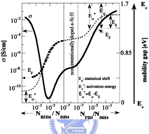
atom is mostly fourfold coordinated, but the bond lengths and angles between the bonds show a wide variation. This structure has a strong impact on the electronic structure of the material. Because the structure is no longer periodic, the strict conservation of momentum does not hold. As a result, instead of the indirect bandgap of crystalline Si, it basically has a direct bandgap. Therefore the absorption coefficient in a-Si:H (1.7 to 1.9 eV) is much higher than that in crystalline Silicon. However, a-Si:H suffer from degradation upon exposure to sunlight [5]. This phenomenon, called the Staebler-Wronski effect, causes a large increase in defect density (strong decrease in excess carrier lifetime), and is reversible upon annealing at temperatures above 150 oC. From values between 1015 and 1016 cm−3 in annealed state, defect densities increase to ~2 x 1017 cm-3 in light-soaked state. The metastable defects are believed to be dangling bonds formed by breaking weak bonds in the random network. The defect densities mentioned are valid for intrinsic amorphous Silicon. Doped amorphous Silicon, obtained by adding diborane to the gas flow for p-type material and phosphine for n-type, contains much more defect than intrinsic a-Si:H (several orders of magnitude higher). Therefore, only intrinsic a-Si:H can be used as an absorber material. Fig. 2-1 shows schematically the results obtained by W. E. Spear et al. [6] by plotting the values of dark conductivity and dark conductivity activation energy Eσ against gas phase doping ratio. Also
plotted is the estimated position of the resulting Fermi level EF, obtained by taking the Eσ
values and correcting for the so-called statistical shift. The key parameters for amorphous Silicon are its dark conductivity, photoconductivity, and its mobility lifetime product. The conductivity of intrinsic a-Si:H in the dark is extremely low (< 10−10 S/cm) because of the low mobility (a-Si:H layer is around 20 cm2/Vs at best), the large bandgap, and the fact that charge carriers at low concentration are trapped at defects. Under illumination, many of the defects get filled with photogenerated carriers and are saturated. As a result, many more charge carriers are available for charge transport, and the conductivity is many orders of magnitude higher than that in the dark. The photoersponse, defined as the ratio of the illuminated
conductivity to the dark conductivity, is a good indication for the suitability of the material for devices, and should be larger than 105.
Fig. 2-1 The dark conductivity σ, activation energy Eσ, and estimated position of Fermi level EF for a-Si:H, as a function of gas phase doping ratio NPH3/NSiH4 (for n-type layers) and NB2H6/NSiH4 (for p-type layers). Eσ* is the estimated ‘true’ distance between band edge (Ec, Ev) and the Fermi level EF, where the statistical shift Es has also been taken into consideration for n-type layers, assuming a constant defect density of 1016 /cm2eV. For p-type layers, an identical correction Es has been assumed. In the graph, the equivalent bandgap of a-Si:H, or the ‘mobility gap’, istaken to be 1.7 eV.
The mobility lifetime (μτ) product is the crucial parameter for the transport properties of excess charge carriers in the layer, and in device grade, amorphous Silicon is larger than 10−7
cm2/V. As a result of the low carrier mobility and low lifetime, collection cannot take place through diffusion. A strong drift field is an absolute requirement. Overall, it is not advisable to use amorphous silicon p–n-type diodes as solar cell structure for three reasons. (1) The doping
capability of a-Si:H is rather poor, the Fermi-level can be pushed only half way towards the conduction and valence band edges, even with heavy doping—this can be seen in Fig. 2-1. (2) Doping has a detrimental effect on a-Si:H layer quality, because it leads to the creation of many additional silicon dangling bonds, which are the main recombination centers in this material. (3) In a classical p–n-type solar cell, carrier collection is obtained by minority carrier diffusion within the p- and n-layers. Diffusion lengths in crystalline silicon wafers are sufficiently high (over 200 μm), to ensure carrier collection over the whole useful range of the solar cell thickness where significant optical absorption takes place. In a-Si:H layers, minority carrier diffusion lengths are extremely small (around 0.1 μm), and it becomes impossible for collection of photogenerated carriers on diffusion. Because of these three reasons, p–i–n diodes are always used for a-Si:H solar cells.
When modeling thin-film silicon devices, it is important to take into account the electronic structures of a-Si:H and μc-Si:H. The spatial disorder in the atomic structure of a-Si:H results in a continuous density of states (DOS) in the band gap with no well-defined conduction-band (CB) and valence-band (VB) edges. When considering the transport properties of charge carriers in a-Si:H, we have to distinguish between the extended states and the localized states in the DOS distribution as sketched in Fig. 2-2. The localized states within the mobility gap strongly influence the trapping and recombination processes; therefore, the trapped charge in the localized states cannot be ignored, as is often the case in the modeling of crystalline semiconductor devices. The localized states in the mobility gap of a-Si:H are represented by the CB and VB tail states and the defect states. These states are different in nature. The tail states behave like acceptor-like states (CB-tail states) or donor-like states (VB-tail states), and their density is described by an exponential decay into the mobility gap. The most common defect in a-Si:H is a dangling bond. A dangling bond can be in three charge states: positive (D+); neutral (D0); and negative (D−). An imperfection with three possible charge states acts to a good approximation like a pair of two imperfections consisting
of a donor-like state (DB+/0) and an acceptor-like state (DB0/−), and is therefore represented by two so-called transition-energy levels E+/0 and E0/− in the band gap. The continuous density of defect states is represented by two equal (Gaussian) distributions located around the middle gap. The corresponding pair of defect energy states is separated by the correlation energy. The different nature of the localized states in a-Si:H requires different approaches for the calculation of recombination-generation (R-G) statistics through these states. The models that are commonly used to describe the localized states in a-Si:H. The energy states in the bandgap act as trapping and recombination centers and therefore strongly affect many electronic properties of a-Si:H and the performance of a-Si:H devices. In contrast to crystalline semiconductors, in which the recombination process is typically dominated by a single energy level in the bandgap, in a-Si:H, contributions from all bandgap states to the recombination–generation (R–G) rate are included. In order to model the recombination process through the single level states, such as localized tail states, Shockley-Read-Hall R–G statistics is applied for the amphoteric defect states.
Fig. 2-2 Density of states of a-Si:H [4].
2.1.2 Single-Junction Microcrystalline Silicon Solar Cells
Microcrystalline is a mixed phase material, containing a crystalline silicon fraction and an amorphous silicon fraction. The crystallites are generally only a few nanometers to a few tens of nanometers in diameters, and are present in “bunches” or“conglomerates” in the layers. These conglomerates are much larger than the crystallites themselves, up to a micron or even larger. Because the crystallites are in the nanometer range, microcrystalline silicon is often referred to as “nanocrystalline silicon”. The two names are nowadays used interchangeably. Like amorphous silicon, microcrystalline silicon contains a lot of hydrogen (several percents), which is incorporated in situ during deposition and ensures passivation of most defects in the layers. The term “microcrystalline silicon” covers, in fact, a whole range of materials, ranging from amorphous silicon with a few percents of crystalline phase to a material with only a few percents of amorphous silicon. The properties of the materials at the two extremes are quite different, and one has to pay attention not to generalize properties that are, in fact, only valid for a limited range of crystallinity. In practice, the best devices are obtained with material close to the edge between microcrystalline and amorphous Silicon, so most recent papers refer to this type of material, which contains a large amorphous fraction. Like amorphous Si, microcrystalline Silicon is typically obtained by PECVD at low temperature (between 100 and 300◦C). Usually, a large hydrogen flow is added, which results in microcrystalline Si instead of amorphous Si (“hydrogen dilution”). The very high frequency (between 30 and 300 MHz) leads to a softer ion bombardment, which is more favorable to microcrystalline Si formation, and, at the same time, allows relatively high growth rates. It is, however, possible to obtain excellent results using the standard RF PECVD technique at 13.56 MHz, provided the right parameters in terms of pressure and gas flow are selected. The conditions used are the so-called “high pressure depletion” (HPD) conditions, where the relatively high pressure (~10 Torr) ensures that ions lose a lot of their energy before reaching the surface. It is important to ensure a high hydrogen content in the plasma in HPD
regime, which is usually obtained by a high hydrogen flow. The combination of Very High Frequency and HPD conditions has led to excellent solar cells. An important aspect for all deposition techniques is the need to control the crystallinity profile of the microcrystalline layer throughout the active layer. As the material is formed through nucleation from an initial amorphous silicon layer after which the crystallites grow, the crystallinity is not constant throughout the layer if no attempt is made to control it, which may result in far from optimal layers. Therefore, research in microcrystalline Silicon deposition puts a lot of effort into crystallinity control during deposition through varying Si the deposition parameters. The bandgap of microcrystalline silicon depends on the fraction of amorphous silicon in the material. Layers with a substantial crystalline fraction have a bandgap close to that of crystalline Silicon (1.1 eV). The apparent higher absorption for such microcrystalline layers compared to single crystalline Si has been demonstrated to be caused by light scattering at the layer surfaces. The absorption below the bandgap is much higher than that for crystalline silicon, and is caused by defects within the bandgap. The absorption coefficient at those long wavelengths, therefore, gives a measure for the layer quality. It can be measured in different ways, but a powerful measurement technique that is increasingly be being used is the Fourier transform photocurrent spectroscopy (FTPS) [7]. Fig. 2-3 also gives important insight in layer quality degradation in microcrystalline silicon. When the first microcrystalline silicon solar cells were demonstrated, tests on devices with relatively high crystallinity led to the conclusion that microcrystalline Silicon did not suffer from light-induced degradation. As better devices closer to the transition were made and more detailed degradation studies were carried out, a more subtle picture has emerged: microcrystalline silicon suffers from a mild form of the photo-induced degradation [8]. The degraded values (after 1000 hours under standard illumination) in Fig. 2-3 show that, as expected, the degradation is worst for fully amorphous silicon, while it is negligible for almost fully crystalline layers. For microcrystalline layers in the transition region, there is a small yet significant degradation.
There is, however, no degradation at all if the high energy photons are filtered out [9], as is the case in tandem solar cells. μc-Si:H with a higher crystalline volume fraction than a-Si:H. The assumption here is that the lower mobility band gap in μc-Si:H thin film cause the lower open circuit voltage. We would expect the free carrier densities to be higher in the bands for the “low Eg” μc-Si:H in which the band edges are closer to the quasi-Fermi levels. This is easily inferred from the expressions of the free carrier densities:
(EC E F n ) / K T C
n
=
N
e
− − Eq. 2-1 (E F p EV ) / K T V p = N e − − Eq. 2-2Fig. 2-3 Defect-related optical absorption in as-deposited and degraded state for a series of single-junction µc-Si:H silicon p-i-n solar cells as a function of the crystallinity of the intrinsic layer (i-layer) [8].
In the general, a μc-Si:H cell with a higher crystallinity has a higher Jsc, primarily because of higher free carrier mobilities and higher free carrier densities, which causes higher photo-generated hole trapping, therefore higher field near the P/I interface, and a collapse of the electric field over the volume and a lower Voc. In fact the above opinions are the reasons
for a lower Voc and higher Jsc in μc-Si:H cells [11].
2.1.3 Tandem Solar Cell
Microcrystalline silicon has not only the advantage of a better stability under light exposure than amorphous silicon. Microcrystalline silicon has a different sunlight absorption spectrum than a-Si:H as shown in Fig. 2-4.
Fig. 2-4 The optical absorption coefficient α and the penetration depth dλ, where dλ = 1/α of monochromatic light with photon energy hυ and wavelength λ, for crystalline silicon (c-Si), and typical device-quality a-Si:H and µc-Si:H layers on glass. The curve
for µc-Si:H has been corrected for light scattering due to surface roughness [10].
µc-Si:H absorbs the light more in the infrared range. This difference between a-Si:H and µc-Si:H has been used to increase the sunlight energy conversion efficiency by performing a so-called Tandem cell, which consists in a multi-junction cell with a top-cell made of a-Si:H and a bottom-cell of µc-Si:H. The thickness of the a-Si:H intrinsic layer is generally thin (about 250 nm) in order to collect a maximum of the photo-induced electrons. The µc-Si:H intrinsic layer has to be thicker (about 1.5 - 2 µm) because of its indirect band-gap and the necessity to match the photo-current generated by the two stacked cells [2].
From the point of view of the manufacturing technique, µc-Si:H is fully compatible with a-Si:H. Indeed, it can be deposited using the same reactor at the same substrate temperature of about 200 ◦C. The source gases are silane and hydrogen as for the deposition of a-Si:H. Generally, the hydrogen dilution is increased to change from the amorphous to the microcrystalline silicon deposition regime. When µc-Si:H is deposited in RF PECVD, the deposition rate (1 - 5 Å/s range) is generally less than for a-Si:H. This low deposition rate is a limiting factor for the use of µc-Si:H in PV solar cells, because it involves a too long time to deposit the ~ 2 µm thick µc-Si:H intrinsic layer. Typically, about 1.5 hours are necessary to deposit a 2 µm thick layer with a 4 Å/s deposition rate. In order to achieve low-cost Tandem PV solar cells, the deposition rate of the intrinsic µc-Si:H layer has to be improved to rates higher than 10 Å/s. High deposition rates are not the only condition for µc-Si:H films to achieve low-cost Tandem PV solar cells. Vetterl et al [12] have shown that the best material quality to be integrated in a Tandem solar cell is at the limit between amorphous and microcrystalline silicon. Therefore, the deposition conditions have to be perfectly controlled in order to have a material crystallinity in the 40 - 60 % range, and not to fall into the fully amorphous or strongly microcrystalline deposition region.
2.2 Deposition Mechanisms of µc-Si:H Thin Film
The mechanisms involved in the growth of hydrogenated microcrystalline silicon are complex, which combine both chemical and physical aspects. The chemical aspects include the hydrogen, silicon dangling bonds and reactions in the film. The physical aspects is such as the species (SiHx and H) bulk diffusion. The heterogeneous microstructure composed by
crystalline grains embedded in an amorphous matrix adds to the system complexity. Moreover, the surface and sub-surface chemistry and physics depend on both the growing film properties and on the plasma. The three most important models are the surface diffusion model, the
selective etching model and the chemical annealing model, which are reviewed in this section.
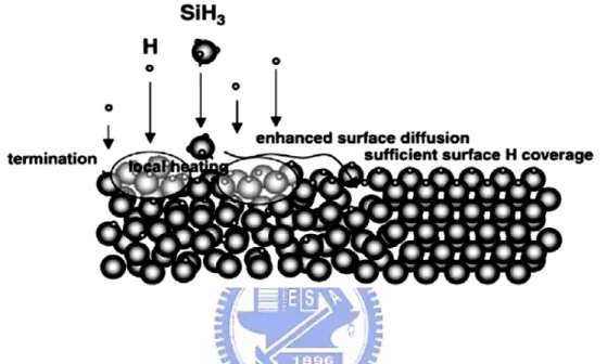
2.2.1 Surface Diffusion Model
The surface diffusion model was experimentally demonstrated as shown by Matsuda [46]. The crystalline volume fraction of deposited films strongly depends on the surface diffusivity of SiHx which is improved when the silane concentration is reduced or the substrate
temperature increased. This is due to the hydrogen surface coverage improvement prolong the SiHx surface diffusion length to permit SiHx to attach at favorable sites to create a flat film
surface. This has been confirmed by the abrupt fall of the film crystallinity for substrate temperature higher than 400 ◦C [13], caused by the desorption of hydrogen adsorbed on the surface at such high temperatures [14]. Moreover, some of the hydrogen atoms coming from the plasma recombine with surface bonded-hydrogen heating locally the surface, which enhances the surface diffusion of SiHx as sketched in Fig. 2-5. The role of the surface
diffusion in flattening the film surface is of particular importance for the nucleation of crystallites as shown by in-situ spectroscopic ellipsometry studies.
They have shown that silicon crystallite nucleation needs a smooth surface and occurs only after a reduction of the initial surface roughness. This shows that to promote the
crystallinity of the deposited silicon film, a sufficiently high atomic hydrogen flux towards the growing film surface has to be delivered with respect to the silicon radicals flux. However, the role of the SiHx surface diffusion in µc-Si:H growth may not be dominant for depositions
performed at high rates, because of the shorter time allowed for SiHx radicals to find adequate
sites to attach.
Fig. 2-5 Schematic representation of the surface diffusion model. The hydrogen atoms from the plasma passivate all the surface dangling bonds, hence enhancing the surface diffusion length of silicon radicals, which have to find an adequate site to attach [15].
2.2.2 Selective Etching Model
The diffusion model was able to explain µc-Si:H deposition for substrate temperatures lower than 400◦C, but µc-Si:H deposition at higher temperatures [16] shows that this model is not sufficient. A combination of the surface diffusion model and selective etching model may explain the deposition of microcrystalline silicon. This selective etching model is based on the experimental observation of silicon etching by hydrogen [17] by the reverse chemical reaction leading to silicon deposition from silane discharge [18].
deposition
4 etching fil
SiH ←⎯⎯⎯⎯⎯⎯⎯⎯→ Si m + 4 H Eq. 2-3
This model is called selective because of the different etching rate of amorphous and microcrystalline silicon [17]. Indeed, the high lattice defect density in the amorphous structure facilitates the atomic hydrogen to etch the silicon atoms which are weakly bonded to their neighbors, whereas the well-arranged silicon atoms of the crystallites resist better to hydrogen etching [15]. The selective etching model sketched in Fig. 2-6 is based on the hypothesis that both amorphous and microcrystalline silicon are deposited and etched simultaneously, but with an etching rate much higher for the amorphous phase, hence increasing the crystalline volume fraction of the growing film. This model has to be combined with the surface diffusion model in order to explain the nucleation of the crystallites to initiate the microcrystalline growth from the initial amorphous incubation layer. As for the surface diffusion model, the crucial physical consideration is the atomic hydrogen flux towards the film surface with regard to the silicon radical flux, in order to etch efficiently the amorphous phase to promote the film crystallinity.
Fig. 2-6 Schematic representation of the selective etching model. The hydrogen atoms from the plasma etch preferentially the amorphous silicon phase, favoring the growth of the crystalline phase, resulting in µc-Si:H [15].
2.2.3 Chemical Annealing Model
The chemical annealing model has been constructed in order to explain the crystallization of amorphous silicon when exposed to a pure H2 plasma [19]. Indeed, µc-Si:H
can be produced by using a layer-by-layer technique by alternatively depositing a thin a-Si:H layer and expose it to a pure H2 discharge which crystallizes the thin layer. Neither the etching
model, nor the surface diffusion model, can explain this phenomenon. This third model is based on the chemical reaction of atomic hydrogen coming from the plasma with hydrogen bonded to silicon at the film surface or sub-surface as depicted in Fig. 2-7. The reaction creates a silicon dangling bond and a hydrogen molecule. This reaction is exothermic, and the resulting structure thermal vibration promotes surface and bulk structural rearrangement leading to the energetically more favorable µc-Si:H [15]. The Si dangling bond created is then transformed into a more stable and rigid Si-Si bond or, if placed at thefilm surface, re-hydrogenated by atomic hydrogen from the plasma. In the selective etching model, the H atoms attach to silicon and re-hydrogenate the bulk silicon until silane desorption. But in the chemical annealing model, the H atoms recombine with surface or sub-surface hydrogen.
Fig. 2-7 Schematic representation of the chemical annealing model. The hydrogen atoms from the plasma recombine with hydrogen bonded to surface or sub-surface silicon atoms, delivering vibrational energy which favors silicon crystallization [15].
Consequently, the atomic hydrogen flow rate towards the surface has to be large compared to the silicon radical flux to promote the growth of µc-Si:H. This is to increase the surface diffusivity by a fully H-covered surface, to remove undesirable a-Si:H by selective etching by H atoms, or to generate vibrational energy by hydrogen surface or sub-surface recombination, according to the surface diffusion, the selective etching or the chemical annealing models, respectively.
Chapter 3
Experimental Technique
3.1 Plasma-Enhanced Chemical Vapor Deposition
The deposition method used to produce the μc-Si:H film is rf (the excitation frequency is 27.12MHz )PECVD. The plasma provides some of the activation energy required for the chemical reaction, in effect reducing the processing temperature required during the film deposition. It is done by collisions with electrons, which originate as secondary electrons in the plasma and build up their energy by acceleration in an electric field. The μc-Si:H film is deposited by attaching reactive particles of dissociated silane molecules, called radicals, to the surface of growing film. Some of the energy transferred to silane molecules in the collisions with electrons is radiated as visible light, for which reason the deposition method is also referred to as glow discharge.
3.2 Raman Spectrum
Fig. 3-1 Micro-Raman spectrometer composed of an He-Ne laser source, a microscope, a notch filter, a grating and a CCD camera [20].
Raman spectroscopy consists in the observation of inelastic scattering of an incident light beam by a media which could be a gas, a liquid or a solid. The Raman effect, first reported by Raman and Krishna in 1928 [20], has been used in this work to evaluate the degree of crystallinity of the deposited silicon layers. The Raman apparatus was a Renishaw RM series with an He-Ne laser source (633 nm).
Silicon films with mixed amorphous-nanocrystalline phase composition, the spectrum consists of a broad low-frequency component peaking around 480 cm-1 and related to the amorphous phase and a substantially narrower peak at 520cm-1 whose increase in intensity indicates nucleation of the nanocrystalline phase. The total scattering intensity I( )ω in the
frequency range under study can be written as the formula.
( )
( )
( ) c a
I ω =I ω +I ω Eq. 3-1 where Ic
( )
ω is the intensity of the line related to the nanocrystalline phase (520cm-1), and(
a
I ω
)
is that of the line associated with the amorphous phase (480 cm-1).Now, considering the relation between the integrated raman intensity and the volume fractions of the amorphous and nanocrystalline phases. This relation is usually written in the Eq. 3-2, where y is the scattering factor.
c a c c a I I X y I I = + Eq. 3-2
An empirical relation for the dependence on Eq. 3.4, We used the value y = 1 [21].
: ( ) 0.1 exp( 25)
L y L = + −L Eq. 3-4
And this is a good agreement with the estimate y=0.88. Thus the formula of crystallinity is described as Eq. 3.5. c c c a I X I I = + . Eq. 3-5 23
Chapter 4
Results and Discussions
4.1 Hydrogenated Amorphous Si Solar Cell
Hydrogenated amorphous Si (a-Si:H) material have received a great attention because of their use in low-cost solar cells. In order to analyze and optimize the performance of thin-film a-Si:H solar cells, it is important to set up an accurate numerical model to simulate the transport mechanisms in the device. Device simulation comprises methods of basic carrier transport and continuity equations for any type of structures defined by two dimensional doping profiles. Silvaco (Atlas), which is based on finite element analysis, is widely used by research institutes and industries. Through Atlas, we input several parameters including: device structure, doping concentration, and bias condition; then, using numerical methods such as: electron and hole current equation, electron and hole continuity equations, and Poisson equation; finally getting the outputs like mobile carriers, electric fields, potentials, and currents in the form of two-dimensional contours and vectors as well as quasi three-dimensional contours. Besides simulating the external current-voltage characteristics, it allows a detailed simulation of physical behaviors of devices in both steady-state and in transient regime. Device simulation has been widely used to study a-Si:H p-b-i-n solar cell performance, which is sensitive to the material properties.
4.1.1 Simulation Model
The physical models that we have used are Klaassen’s concentration dependent SRH model (KLASRH), Klaassen’s Auger model (KLAAUG), Klaassen’s concentration dependent lifetime model, and Klaassen’s low field mobility model (KLA). The photo-generation model which includes a ray tracing algorithm is used to calculate the transmission and absorption of light in the bulk as well as reflection and refraction at the interfaces. The p-i-n solar cell is
operated under the global standard solar spectrum (AM 1.5G) illumination with total incident power density which is 100 mW/cm2 and the light intensity for each wavelength is calculated in the wavelength from 0.3 to 1.2 μm. A structure consists of flat glass/ITO/a-Si:H p-i-n/Ag, is considered as the solar cell model for simulation, in which light penetrate through the p-layer. The figure is shown as Fig. 4-1.
Fig. 4-1 Schematics of an a-Si solar cell structure, which consists of glass/ITO/a-Si:H p-i-n/Ag
We set the solar cell in length and width both as 1 μm . The thicknesses of i-layer is 450 nm. We assumed that interfaces are all flat for this simulation. The doping concentration of p- and n-type set as 3x1018 cm-3 and 9x1018 cm-3at first. Each dangling bond density in
p-layer and n-layer is set as 5x1018 cm-3 and 9x10¹⁸ which is higher than that in other layers. It is because the dangling bond density would increase with higher doping concentration in a-Si:H material. Also, we have analyzed the effect of light soaking would increase dangling bond density (Ndb) in a-Si:H layer. The electrical, optical, and structural parameters in the
Table 4-1 which were adapted from the literature [22, 23] are used for simulating the device performance. The distribution of density of states (DOS) in the forbidden energy gap of undoped a-Si:H i-layer is used in the simulation.
Table 4-1 Device Parameters of a-Si:H solar cell used in Simulations.
Parameter p-a-SiC:H b-a-SiC:H i-a-Si:H n-a-Si:H
Layer thickness (nm) 5~20 1~10 250~500 10~30
Mobility gap (eV) 2 1.96 1.86 1.8
Donor doping density (cm-3) 3x10¹⁸
acceptor doping density (cm-3) 9x10¹⁸
Electron mobility(cm2/V s) 20 20 20 20
Hole mobility(cm2/V s) 4 4 4 4
Electron life time (μs) 0.01 0.01 0.01 0.01
Hole life time (μs) 0.1 0.1 0.1 0.1
Effective DOS in the valance and conduction bands (cm-3)
2x10²⁰ 2x10²⁰ 2x10²⁰ 2x10²⁰ Exponential tail Prefactors NTD, NTA
(cm-3eV-1)
4x10²¹ 4x10²¹ 4x10²¹ 4x10²¹ Characteristic energy WTD (VB tail) (eV) 0.12 0.11 0.08 0.05 Characteristic energy WTA (CB tail) (eV) 0.07 0.055 0.05 0.03 Gaussian distribution density NGD, NGA
(cm-3eV-1)
5x10¹⁸ 5x10¹⁷ 5x10¹⁵ 9x10¹⁸ Characteristic energy for Gaussian
distribution WTD (donor like state) (eV)
0.2 0.2 0.2 0.2
Characteristic energy for Gaussian distribution WTA (acceptor like state) (eV)
0.2 0.2 0.2 0.2
Peak of donor like Gaussian distribution EGD (eV)
0.8 0.82 0.83 0.78
Peak of acceptor like Gaussian distribution EGA (eV)
0.9 0.67 0.67 0.52
Correlation energy U (eV) 0.3 0.47 0.36 0.5
Transmittance of glass / ITO 0.9
Reflectivity of n layer / metal contact 0.9
Surface recombination velocity 1x10⁷ 1x10⁷
a measured from the conduction band edge ; b measured from the valance band edge
Fig. 4-2 is the general standard model for DOS of a-Si:H i-layer and is described by : 1. A parabolic conduction band and exponentially decaying conduction band tail.
( ) exp C TA E E g E NTA WTA − ⎡ ⎤ = ⎢ ⎥ ⎣ ⎦ Eq. 4-1 2. A parabolic conduction band and exponentially decaying conduction band tail.
( ) exp V TD E E g E NTD WTD − ⎡ = ⎢⎣ ⎦ ⎤ ⎥ Eq. 4-2 3. Two equal Gaussian distributions of states around the middle gap separated from each
other by a correlation energy (U) for representing the defect state related to dangling bonds (DB+/0 and DB0/-). 2 ( ) GA EGA E g E NGA WGA ⎡ ⎡ − ⎤ = ⎢− ⎤ ⎥ ⎢⎣ ⎦⎥ ⎢ ⎥ ⎣ ⎦ Eq. 4-3 2 ( ) GD E EGD g E NGD WGD ⎡ ⎡ − ⎤ = ⎢−⎢⎣ ⎤ ⎥ ⎦⎥ ⎢ ⎥ ⎣ ⎦ Eq. 4-4
Fig. 4-2 Distribution of acceptor/donor-like trap states across the forbidden energy gap used in i-layer in the simulation.
The device performance of the a-Si:H solar cell is studied by using Atlas. The electric characteristics of a-Si:H solar cell are as following:
Fig. 4-3 The illuminated J-V characteristic curve of a-Si:H p-i-n solar cell
The computer simulation of a-Si:H p-i-n solar cell was carried out by atlas. The short circuit current (Jsc), open circuit voltage (Voc), fill factor (FF), and the efficiency of a-Si:H
solar cell are 13.3 mA/cm-2 , 0.83V, 0.74, and 8.37 %, respectively in Fig. 4-3. We considered the lower efficiency resulted from two reasons. First, the flat interfaces would reduce the light refraction and reflection. Second, the lack of TCO between the n-layer/Ag interface also made the efficiency low. The performance of the cell within light soaking effect is analyzed by increasing Ndb from 5x1015 cm-3 to 5x1018 cm-3 as shown in Fig. 4-4 and Fig. 4-5. The
open-circuit voltage Voc, fill factor FF, and short-circuit density Jsc were all decreased due to
the Ndb increased. a-Si:H would degrade upon exposure to sunlight. This phenomenon, called
the Staebler-Wronski effect or light soaking effect, causes large increases in defect density and is reversible when annealed at temperatures above 150 oC. The metastable defects are
believed as dangling bonds formed by breaking weak bonds in the random network. In order to eliminate this effect, reducing i-layer thickness and hydrogen content in the film are two better ways so far. Thus, the a-Si:H i-layer of tandem solar cell is also designed to be thinner to achieve this purpose.
Fig. 4-4 Photovoltaic performance of a-Si:H solar cell with different Ndb of i-layer.
Fig. 4-5 The J-V characteristics curve with different Ndb in i layer of a-Si:H cells.
4.2 Microcrystalline Silicon solar cell
The structure of microcrystalline p-i-n solar cell is as following: flat ITO/p-μc-Si:H / i-μc-Si:H/n-a-Si:H/Ag. The open-circuit voltage, short-circuit current density, and the fill factor determine the output properties of a solar cell; however, unlike the other two parameters, the behavior of the open-circuit voltage (Voc) is not easy to be understood. It is
well known the Voc in hydrogenated microcrystalline silicon (μc-Si:H) thin-film solar cell
declines sharply when the crystalline fraction increases from 60% to 90% or even higher. The tendency of different crystallinities of μc-Si:H cells has been studied until now, but it still lacks detailed quantification of the impact of individual material properties on solar cells. Here, we used a powerful electrical-optical computer modeling program (Atlas) to simulate the optimal μc-Si:H thin-film solar cells to understand the difference between the a-Si:H and μc-Si:H solar cell.
4.2.1 Simulation Model
The μc-Si:H solar cell structure is shown as Fig. 4-6. The length and width of solar cell are both set as 1 μm . The thicknesses of i-layer is 2200 nm. We assumed that interfaces are all flat in this simulation. Each doping concentration of p- and n-type initially set as 1x1019 cm-3and 3x1018 cm-3to optimize cell performance.
Fig. 4-6 μc-Si:H solar cell structure.
To model all aspects of the solar cell performance accurately, we had to assume that the more crystallized material has a lower band gap, higher carrier mobilities, and both higher mid-gap defect density and narrower band tails. A lower band gap for more crystallized μc-Si:H has been previously measured [24] by in situ Kelvin probe analysis and the “Flat Band Hetero-junction” technique; it also measured by photoluminescence (PL) in the study of Merdzhanova et al. [25] . In a-Si:H, the bonding length and bonding angle altered slightly but still in rule in short range, whereas atoms arrange randomly in long range. It makes the tail distribution is broader than the crystalline material. The physical simulation model are
Klaassen’s concentration dependent SRH model (KLASRH), Klaassen’s Auger model (KLAAUG), Klaassen’s concentration dependent lifetime model, and Klaassen’s low field mobility model (KLA).
Table 4-2 Device Parameters of μc-Si:H solar cell used in Simulations.
Parameter p-μc-Si:H b-μc-Si:H i-μc-Si:H n-a-Si:H Layer thickness (nm) 10~30 5~10 1500~2500 10~20
Mobility gap (eV) 1.2 1.4 1.4 1.8
Donor doping density (cm-3) 3x10¹⁸
acceptor doping density (cm-3) 1x10¹⁹
Electron mobility(cm2/Vs) 100 32 32 20
Hole mobility(cm2/Vs) 25 8 8 4
Electron life time (μs) 0.01 0.01 0.01 0.01
Hole life time (μs) 0.1 0.1 0.1 0.1
Effective DOS in the valance and
conduction bands (cm-3) 2x10
20 2x10²⁰ 2x10²⁰ 2x10²⁰ Exponential tail Prefactors NTD, NTA
(cm-3eV-1)
4x10²¹ 4x10²¹ 4x10²¹ 4x10²¹ Characteristic energy WTD (VB tail) (eV) 0.04 0.045 0.05 0.05 Characteristic energy WTA (CB tail) (eV) 0.02 0.025 0.03 0.03 Gaussian distribution density NGD, NGA
(cm-3eV-1) 5x10
18 3x10¹⁷ 4x10¹⁶ 9x10¹⁸ Characteristic energy for Gaussian
distribution WGD (donor like state) (eV) 0.2 0.2 0.2 0.2 Characteristic energy for Gaussian
distribution WGA (acceptor like state) (eV) 0.2 0.2 0.2 0.2 Peak of donor like Gaussian distribution
EGD (meas. From Valance edge) (eV) 0.4 0.7 0.7 1 Peak of acceptor like Gaussian distribution
EGA(meas. From Conduc. edge) (eV) 0.6 0.5 0.5 0.6
Correlation energy U (eV) 0.2 0.2 0.2 0.2
Transmittance of glass / ITO 0.9
Reflectivity of n layer / metal contact 0.9
Surface recombination velocity 1x10⁷ 1x10⁷
a measured from the conduction band edge ; b measured from the valance band edge
The photogeneration model, which includes a ray tracing algorithm, is used to calculate the transmission and absorption of light in the bulk as well as reflection and refraction at the interfaces. The μc-Si:H solar cell is operated under the global standard solar spectrum (AM 1.5G) illumination with 100 mW/cm2 total incident power density and the light intensity for each wavelength is calculated in the wavelength ranger from 0.3 to 1.2 μm. Table 4-2 indicates electrical, optical and structural parameters used for simulating the device performance [26].
Fig. 4-7 Distribution of acceptor/donor-like trap states across the forbidden energy gap used in i-layer in the simulation study.
Fig. 4-7 is the general standard model for DOS of μc-Si:H i-layer. We assumed the Gaussian defect density in μc-Si:H i-layer is 4x1016 cm-3 which is higher than in a-Si:H i-layer (5x1015 cm-3), because the defects fill with the grain boundaries. Due to the μc-Si:H material, it makes lower band gap, sharper band tails and higher Gaussian defect density. Simulation
results indicate a higher Jsc but lower Voc in higher crystallinity material as shown in Fig. 4-8.
The short current ,open voltage, fill factor, and the efficiency of a-Si:H solar cell are 21.81
mA/cm2, 0.47V, 0.73, and 7.49 %, respectively. As we have stated, the electrical
characteristics are differ from the a-Si:H solar cell in Table 4-3. The crucial point to reach solar grade quality µc-Si:H is to have good quality grain boundaries containing a low amount of unstable defects. Indeed, low quality amorphous silicon grain boundaries or cracks along grain boundaries which can be observed in highly-crystalline µc-Si:H.
Fig. 4-8 The illuminated J-V characteristic curve of μc-Si:H p-i-n solar cell
Table 4-3 The electrical characteristics for a-Si:H and μc-Si:H solar cells.
Description Jsc (mA/cm2) Voc (V) FF Efficiency (%)
a-Si:H solar cell 13.3 0.83 0.74 8.37
μc-Si:H solar cell 21.81 0.47 0.73 7.49
4.3 Tandem Solar Cell with and without x Layer
The Tandem solar cell is constituted by the optical and electrical series connection of an amorphous silicon (a-Si:H) top cell and a microcrystalline silicon (µc-Si:H) bottom cell. As a consequence of the electrical series connection, the short-circuit current density Jsc of the
whole tandem is limited by the absorber (top or bottom cell) with the lower current generation capabilities. The thickness of the a-Si:H intrinsic layer must be made as thin as possible to minimize the Staebler-Wronski effect. It is generally thin (about 250 nm) in order to collect a maximum of the photo-induced electrons. The µc-Si:H intrinsic layer has to be thicker (about 2 µm) because of its indirect band-gap and the necessity to match the photo-current generated by the two stacked cells.
Fig. 4-9 Tandem solar cell without x layer.
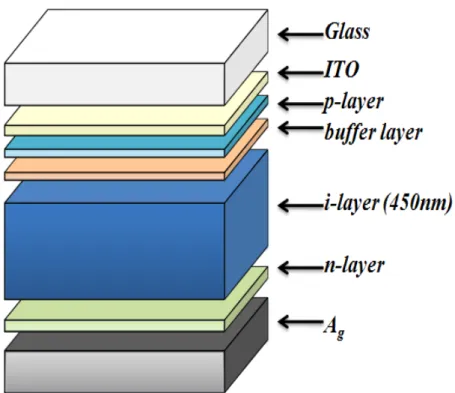
Tandem solar cell with the following structure as shown in Fig. 4-9 was used in the simulations: flat glass / ITO / p-a-SiC:H / i-a-Si:H(di,top) / n-a-Si:H / p-µc-Si:H /
i-µc-Si:H(di,bot) / n-a-Si:H / Ag. The Ag forms the BR. The absorber layers were relatively
thin (di,top 200 nm and di,bot 2.2µm), and no interlayer was applied. The calibrated optical and
electrical parameters of undoped, doped a-Si:H and µc-Si:H layers were used in the simulations.
4.3.1 Simulation Model
Since the tandem cell was fabricated under the same conditions as the single-junction cells we used this set of parameters for modeling of the tandem cells. Also, The physical models we used here are identical with a-Si:H and µc-Si:H solar cell as mentioned before except thickness.
Fig. 4-10 Tandem solar cell with x layer.
The physics controlling the electric transport in n-a-Si:H and p-µc-Si:H interface is generally called tunneling recombination junction (TRJ) as shown in Fig. 4-9 which is
explored with atlas. When modeling the tandem cell as a complete stacked structure (pinpin device), and not using a x layer for the TRJ between the two-component cells, we could not obtain an realistic J-V curve for illuminated tandem cell unless adding a strong-recombination layer (which we call an x-layer) sandwiched between the n- and p-layers of the two inter-cell contact regions as shown in Fig. 4-10. We also have found that the parameters of the TRJ, such as doping concentration and the defect density in the doped layers of the TRJ, must be optimized in order to get the realistic illuminated characteristics of the tandem cell. The parameters for models, such as the mobility gap and the defect density of the x-layer, were also sensitive for obtaining the realistic tandem cell characteristics. After determining the parameters of the TRJ models, we obtained an excellent J-V curve of tandem cell with added-x-layer models. A typical J-V curves for both cases (with and without x layer) are shown in Fig. 4-11.
Fig. 4-11 The J-V curves of tandem solar cells with and without x layer.
![Fig. 1-1 Panel of the different PV technologies with their conversion efficiencies, from high performance multi-junction GaInP/GaAs/Ge to very low cost chemical dye sensitized cells [13]](https://thumb-ap.123doks.com/thumbv2/9libinfo/8755957.206908/13.892.129.761.124.761/different-technologies-conversion-efficiencies-performance-junction-chemical-sensitized.webp)
![Fig. 2-2 Density of states of a-Si:H [4].](https://thumb-ap.123doks.com/thumbv2/9libinfo/8755957.206908/22.892.155.791.506.1131/fig-density-states-si-h.webp)
![Fig. 2-3 Defect-related optical absorption in as-deposited and degraded state for a series of single-junction µc-Si:H silicon p-i-n solar cells as a function of the crystallinity of the intrinsic layer (i-layer) [8]](https://thumb-ap.123doks.com/thumbv2/9libinfo/8755957.206908/25.892.189.704.473.1012/optical-absorption-deposited-degraded-junction-function-crystallinity-intrinsic.webp)
![Fig. 2-6 Schematic representation of the selective etching model. The hydrogen atoms from the plasma etch preferentially the amorphous silicon phase, favoring the growth of the crystalline phase, resulting in µc-Si:H [15]](https://thumb-ap.123doks.com/thumbv2/9libinfo/8755957.206908/30.892.150.777.493.973/schematic-representation-selective-hydrogen-preferentially-amorphous-crystalline-resulting.webp)
![Fig. 2-7 Schematic representation of the chemical annealing model. The hydrogen atoms from the plasma recombine with hydrogen bonded to surface or sub-surface silicon atoms, delivering vibrational energy which favors silicon crystallization [15]](https://thumb-ap.123doks.com/thumbv2/9libinfo/8755957.206908/31.892.177.764.768.1024/schematic-representation-annealing-recombine-hydrogen-delivering-vibrational-crystallization.webp)
![Fig. 3-1 Micro-Raman spectrometer composed of an He-Ne laser source, a microscope, a notch filter, a grating and a CCD camera [20]](https://thumb-ap.123doks.com/thumbv2/9libinfo/8755957.206908/33.892.126.783.495.1070/micro-raman-spectrometer-composed-source-microscope-filter-grating.webp)
![Table 4-1 which were adapted from the literature [22, 23] are used for simulating the device performance](https://thumb-ap.123doks.com/thumbv2/9libinfo/8755957.206908/37.892.144.745.296.1083/table-adapted-literature-used-simulating-device-performance.webp)
