國 立 交 通 大 學
光電工程研究所
博士 論 文
閘極介電層於矽通道與鍺通道
金氧半場效電晶體之研究
Study of Thin Gate Dielectrics on Silicon and Germanium
MOSFETs
研 究 生 :黃震鑠
指導教授 :劉柏村 博士
Chen-Shuo Huang
Dr. Po-Tsun Liu
中 華 民 國 一百 年 九 月
閘極介電層於矽通道與鍺通道
金氧半場效電晶體之研究
Study of Thin Gate Dielectrics on Silicon and
Germanium MOSFETs
研 究 生:黃震鑠
指導教授:劉柏村 博士
Student: Chen-Shuo Huang
Advisor: Dr. Po-Tsun Liu
國 立 交 通 大 學
光電工程研究所
博士 論 文
A Dissertation
Submitted to Institute of Electro-Optical Engineering Department of Photonics
College of Electrical and Computer Engineering National Chiao Tung University
in Partial Fulfillment of the Requirements for the Degree of
Doctor of Philosophy in
Electro-Optical Engineering September 2011
Hsinchu, Taiwan, Republic of China
閘極介電層於矽通道與鍺通道
金氧半場效電晶體之研究
研究生:黃震鑠
指導教授:劉柏村 博士
國立交通大學
光電工程研究所
摘要
本論文探討閘極介電層於矽型與鍺型場校電晶體的應用。本文首先討論氮輪廓分佈 (Nitrogen profile)與記憶應力記憶技術(stress memorization technique, SMT)於超薄氮氧化 矽介電層於 45 奈米矽型場效電晶體之影響。在氮輪廓分佈於超薄氮氧化矽介電層的研 究中,發現即使具有相同等效氧化層厚度的氮氧化矽介電層,其氮輪廓分佈仍會對閘極 穿隧漏電流造成影響。而且閘極穿隧漏電流隨著氮輪廓分佈越傾斜而越大。另外相較於 負型(n-type)場效電晶體,正型(p-type)場效電晶體增加的幅度更大。本文以 WKB 近似為 理論基礎,建立一直接穿隧漏電流物理模型。此模型透過建立介電常數、能帶彎曲程度 與有效載子穿隧質量對於氮輪廓分佈變化而得以合理解釋氮輪廓分佈對於正負型場效 電晶體的影響。另外在記憶應力記憶技術於超薄氮氧化矽介電層研究中,本文發現異常的閘極漏電流因記憶應力記憶技術增加。本文利用載子分離量測法,鑑定出異常的閘極 漏電流來自於載子經由閘極流向源極/汲極區。另外本文亦發現記憶應力記憶技術會導致 閘極與源極/汲極的耦合電容增加的現象。實驗結果顯示高伸張應力導致源極/汲極的輕 摻雜區(LDD)因而延伸與邊際閘極區域破壞,並引起異常高閘極穿隧漏電流。 在閘極介電層於鍺型場校電晶體的研究中,本文提出以高壓水方式對鍺型元件施予 處理。為了清楚釐清高壓水對於鍺型元件中的各層薄膜的影響,本文逐步在二氧化矽於 鍺基板研究高壓水對鍺基板的影響;在二氧化鋯於矽基板中研究高壓水對二氧化鋯的影 響;最終實現高壓水對二氧化鋯於鍺基板處理。在二氧化矽於鍺基板研究中,經高壓水 處 理 後 的 元 件 顯 示 出 較 平 坦 的 表 面 特 性 與 抑 制 電 容 - 電 壓 中 頻 率 發 散 (frequency dispersion)現象。而且本文發現以高壓水處理經高溫退火後的元件可以降低其漏電流。 在二氧化鋯於矽基板的研究中,經高溫退火處理後的元件會因二氧化鋯結晶而導致漏電 上升。經過高壓水處理後的元件,其閘極漏電流、電容遲滯現象(hysteresis)和等效電容 厚度(capacitance-equivalent thickness, CET)明顯下降。其推斷源自於二氧化鋯中晶粒的 缺陷與靠近矽基板的邊緣缺陷(border traps)經高壓水處理而被修復。最後研究高壓水對 二氧化鋯於鍺基板上的影響。本研究發現以高壓水處理二氧化鋯於鍺基板的元件,可消 除介於二氧化鋯和鍺基板中間層形成物-低氧化鍺(Ge suboxide)。在沉積或熱製程所形成 的低氧化鍺會造成閘極漏電增加,也會使閘極控制能力下降。 電子能譜儀 (X-ray photoelectron spectroscopy) 和 高 解 析 度 場 效 電 子 顯 微 鏡 (high-resolution transmission
制主要由於水氧化未完全氧化的氧化鋯,並其所生成的氫進一步與低氧化鍺還原成鍺。 而且經高壓水處理後,二氧化鋯-鍺電容元件的閘極漏電流下降 1000 倍。 除此之外,本論文也在快速爐管退火製程中添加水和氫氣,並研究其對二氧化鋯於 鍺基板的影響。實驗結果顯示,在適當的退火溫度下添加水與氫氣可有效地抑制低氧化 鍺的生成並抑制閘極漏電流。但是當快速退火爐管製成達到 500 度時,氫氣會因劇烈的 氧化還原反應造成鍺表面不平整,甚至出現孔洞現象。
Study of Thin Gate Dielectrics on Silicon and
Germanium MOSFETs
Student:Chen-Shuo Huang
Advisor:Po-Tsun Liu
Department of Photonics and Institute of Electro-Optical Engineering
College of Electrical and Computer Engineering
National Chiao Tung University
Abstract
This work focuses on characterization of thin gate dielectrics on silicon (Si) and
germanium-based (Ge-based) metal-oxide-semiconductor field-effect transistor (MOSFET).
First, the impacts of nitrogen profile (N profile) and stress memorization technique (SMT) on
ultrathin oxynitride (SiON) for 45-nm Si-based MOSFETs application are investigated. The
dependence of the gate tunneling current (JG) on N profile within an ultrathin SiON film was
observed. It was found that gate tunneling current is dependent on N profile, even with equal
oxide thickness and nitrogen dosage. Gate tunneling current increased with steeper N profile,
described the influence of N profiles on gate tunneling current through local change of
dielectric constant, band bending, and effective mass. Also, it reasonably explained the
different JG sensitivity in n-/p-MOSFETs, a phenomenon that has not been addressed in earlier
publications. Then, anomalously high gate tunneling current, induced by high tensile SMT is
reported in this work. Carrier-separation measurement method shows the increased gate
tunneling current is originated from the higher gate-to-source/drain tunneling current, which
worsens when channel length is getting shorter. Also, the device with enhanced tensile strain
exhibits 9% higher gate-to-source/drain overlapping capacitance. These data indicate the
anomalously high gate tunneling current could be attributed to the high tensile strain that
induces the effects of excessive lightly-doped drain-source (LDD) dopant diffusion and higher
gate edge damage. The proposed inference is confirmed by channel hot electron stress.
Then, high-pressure (HP) H2O treatment at low temperature (100~150 °C) has been
proposed to treat Ge MOS devices. The effect of high-pressure H2O treatment on Ge MOS
devices is examined step-by-step to discriminate the influence on individual layer within Ge
MOS capacitor. The HP H2O treatment was respectively performed on SiO2/Ge stack for
exploration of Ge substrate, on ZrO2/Si for exploration of ZrO2 thin film and finally realized
on ZrO2/Ge capacitors. In the investigation of SiO2/Ge MOS devices, a smooth interfacial
GeO2 layer between gate SiO2 and Ge is formed after H2O treatment, and the frequency
the electrical degradation of Ge-MOS after a post-gate dielectric annealing at 450 °C can be
restored to an extent similar to the initial state. In the investigation of ZrO2/Si MOS devices,
the dramatic increase of JG for ZrO2 dielectrics after rapid thermal annealing (RTA) at 500 °C
was found and attributed to defective grain boundaries induced by thermal crystallization.
After high-pressure H2O treatment, the hysteresis, gate leakage current and
capacitance-equivalent thickness (CET) reduces in ZrO2/Si capacitor. It is inferred that the
HP H2O treatment passivates the border traps in ZrO2 nearby Si substrate and defective
grain boundary regions in the bulk of ZrO2. The HP H2O treatment was finally realized on
the sputtered ZrO2 upon Ge substrate. This investigation demonstrates the effect of HP H2O
treatment on the elimination of the interfacial germanium suboxide (GeOX) layer between
ZrO2 and Ge. The formation of GeOX interlayer increases the gate leakage current and worsen
the controllability of the gate during deposition or thermal cycles. X-ray photoelectron
spectroscopy and high-resolution transmission electron microscopy reveal that HP H2O
treatment eliminates the interfacial GeOX layer. The physical mechanism involves the
oxidation of non-oxidized Zr with H2O and the reduction of GeOX by H2. Treatment with H2O
reduces the gate-leakage current of a ZrO2/Ge capacitor by a factor of 1000.
In the other way, the effects of H2O and H2 ambiences for RTA system on sputtered ZrO2
upon Ge substrate are reported in this work. The experimental results reveal that H2O or H2 in
current at appropriate process temperature. However, when the temperature of RTA treatment
reaches at 500 °C, the aggressive oxidation-reduction reaction in H2 ambience cloud cause
誌謝
在此篇論文完成之際,我開始回想所經歷過的研究生涯。回想當初繼續攻讀博士學 位的原因,只是一個簡單的理由:因為我還有許多不懂,想再多了解一些。而在經過這些 年後,再度檢驗自己,覺得自己好像多懂了一些,但是好像又發掘更多不明瞭之處,這 才知道原來科學是這麼深奧與廣大,而自己的研究只是眾多領域中之小小一處,更體悟 到一人之力難成大事。首先,感謝多年來細心指導我的劉柏村教授,感謝劉老師在學術 上的指導,總是在學涯迷惘時給予適當貼切的提攜;感謝劉老師給予相當大的空間,能 盡情發揮所學,讓學生勇敢嘗試;感謝劉老師提供許多機會,讓學生具有業界實務經驗, 了解業界與學界差異性,並提供平台讓兩者融合;另外,因劉老師而所聚集的實驗室大 家庭,形成的舒適研究環境,使得學生能快樂在這個地方學習。 感謝中山大學物理系啟蒙老師張鼎張教授,感謝您引領進門並常仔細講解薄膜電晶 體相關知識。感謝先前在台灣積體電路製造有限公司提供實習機會的陳啟群博士、林秉 順博士與李達元博士,因為有你們帶領才能讓我對半導體製程有更深的了解,更因與你 們一同討論才能觸及更深的研究。感謝曾鈺芬博士一同討論材料分析與化學觀念。 另外要感謝實驗室的夥伴們:竹立煒、鄧立峯、黃羿霖、傅治翔、鄭光廷與范楊順, 有你們在艱難的研究生涯裡點上色彩,我會一直懷念實驗室的種種。感謝一起共事過的 學弟妹聶建銘、鐘宛芳、黃千睿、楊維哲、林敬儒、吳明聰、王薇雅與許沁卉,感謝你 們在研究上參與討論與貢獻。另外也感謝認識至今已超過十年的大學好友許書偉、王萬倉、李泓緯、李國昶、林建宇、凌嘉駿、劉昇旭、康玉清、林宏偉與吳元均,感謝你們 在人生路上困難相挺與熱情相伴,年度出遊常讓我心靈獲得舒放。 最後感謝我的家人惠珍、大姐馨怡與二姐郁雅的精神支持與鼓勵。並由衷感謝我的 父親黃文宏先生與母親黃簡綉英女士,感謝撫育之恩與疼惜之情,感謝父親於幼時的循 循善誘並開啟往研究之路,於青少年莽撞時期所賦予的耐心,並與母親體諒與一路支持 至攻讀博士學位,恩情無以言喻。
Contents
Abstract (Chinese) ... i Abstract ... v Acknowledgement (Chinese) ... ix Contents ... xi Figure Captions ... xv Tables ... xxiii Chapter 1 Introduction ... 11.1 Revolution and challenges of gate dielectric on Si-MOSFETs ... 1
1.2 Revolution and challenges of gate dielectric on Ge-MOSFETs ... 4
1.3 Motivation ... 6
1.4 Organization of the thesis ... 7
Chapter 2 Experiments ... 15
2.1 High-pressure H2O system ... 15
2.2 X-ray photoelectron spectroscopy ... 16
2.3 Parameter extraction ... 18
Chapter 3 Ultrathin Nitrided Oxides for Si-based MOSFET ... 25
3.1 Review and motivation ... 25
3.2 Modeling of nitrogen profile effects on ultrathin nitrided oxides ... 26
3.3 Effect of high tensile stress on ultrathin nitrided oxides ... 31
3.4 Summaries ... 35
Chapter 4 Effect of High pressure H2O on Gate Dielectric for Ge MOSC ... 49
4.1 Review and Motivation ... 49
4.2 Effect of high-pressure H2O treatment on SiO2/Ge stack ... 51
4.3 Characteristics of ZrO2 thin film on Si substrate ... 57
4.4 Effect of High-Pressure H2O Treatment on ZrO2/Ge Stack ... 60
Chapter 5 Effect of Water Vapor and Hydrogen Annealing on ZrO2/Ge Stack ... 87
5.1 Review and motivation ... 87
5.2 Device fabrication ... 87
5.3 Results and discussion ... 88
5.4 Summaries ... 94
Chapter 6 Summaries and Future Work ... 111
6.1 Summaries ... 111
Reference ... 115
Appendix ... 129
A.1 Impact of Negative-Bias-Temperature-Instability on channel bulk of polysilicon TFT by gated PIN diode analysis ... 129
A.2 Enhanced NBTI degradation by SMT in short-channel pMOSFET ... 135
Curriculum Vitae ... 149
Figure Captions
Chapter 1
Figure 1-1 Logic technology node and transistor gate length versus calendar year.[1] ... 10
Figure 1-2 Transistor cost and lithographic tool cost versus years.[1] ... 11
Figure 1-3 Gate-current density against effective-oxide thickness with various gate
materials.[7] ... 12 Figure 1-4 Correlation of dielectric constant with band gap of candidate [8]. ... 13
Chapter 2
Figure 2-1 The high-pressure H2O system. ... 21
Figure 2-2 The pressure and temperature phase diagram of CO2. ... 22
Figure 2-3 The plot of density variation with respect to pressure and temperature for CO2.[29] ... 23
Figure 2-4 The ionic product of water at high temperature and high pressure.[29] ... 23 Figure 2-5 The example of binding energy shift with oxide formation.[32] ... 24 Chapter 3
Figure 3-1 Comparison of nitrogen depth profile for two kinds of SiON films with similar thicknesses and nitrogen concentrations. ... 36 Figure 3-2 Gate current density against capacitance effective thickness with different
Figure 3-3 Band offset of SiON to Si with various dose of nitrogen. ... 38 Figure 3-4 Schematic showing for two kinds of N profiles: the steep vs. the smooth
profile. ... 39 Figure 3-5 Simulated energy band diagram for steeper and smooth N-profile without gate
bias. ... 39 Figure 3-6 Simulated energy band diagram for steeper and smooth N-profile with (a)
positive and (b) negative gate bias. ... 40 Figure 3-7 Tunneling probability and tunneling probability ratio for electrons and holes
under various biasing conditions. ... 41 Figure 3-8 The gate leakage current density for nMOSFET and pMOSFET under various
bias conditions. ... 42 Figure 3-9 The transfer characteristics of nMOSFET with high and low tensile strain. ... 43 Figure 3-10 The mobility of n/pMOSFET with different tensile strain. ... 43 Figure 3-11 The plot of gate current density (Jg) against the gate biases. ... 44
Figure 3-12 (a) Schematic diagram of leakage path, (b) band diagram of gate to S/D and (c) band diagram of gate to substrate under low negative gate bias.. ... 45 Figure 3-13 (a) Schematic diagram of leakage path and (b) band diagram of gate to
substrate under high negative gate bias. ... 46 Figure 3-14 Dependence of JG on device channel length. ... 47
Figure 3-15 Gate-to-S/D overlap capacitance. ... 47 Figure 3-16 Linear-mode transfer characteristics for both Sample A and Sample B. ... 48 Chapter 4
Figure 4-1 The cross-sectional HRTEM images of LPCVD-SiO2 on epi-Ge substrate (a)
before and (b) after high-pressure H2O treatment. ... 67
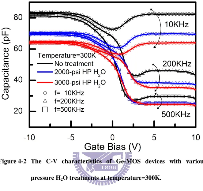
Figure 4-2 The C-V characteristics of Ge-MOS devices with various pressure H2O
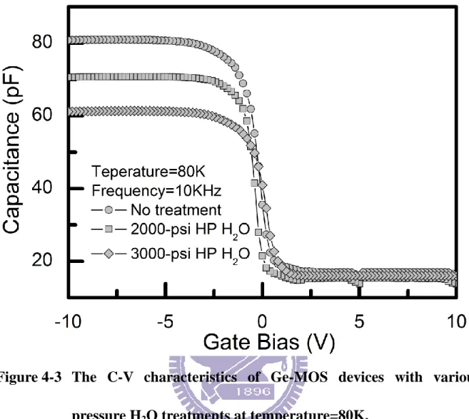
treatments at temperature=300K. ... 68 Figure 4-3 The C-V characteristics of Ge-MOS devices with various pressure H2O
treatments at temperature=80K. ... 69 Figure 4-4 XPS spectra of Ge 3d signal of HfO2 on the epi-Ge channel layer with and
without HP H2O treatment. ... 70
Figure 4-5 The C-V characteristics of 450 °C PDA-treated Ge-MOS devices before and after HP H2O treatment. ... 71
Figure 4-6 The gate leakage current density of PDA-treated Ge-MOS devices before and after HP H2O treatment. ... 72
Figure 4-7 The gate leakage current density of sputtered-ZrO2 on Si with various thermal
treatments. ... 73 Figure 4-8 The gate leakage current density of sputtered-ZrO2 on Si with 500 °C RTA
Figure 4-9 The C-V characteristics of sputtered-ZrO2 on Si with various thermal
treatments. ... 75 Figure 4-10 The C-V characteristics of sputtered-ZrO2 on Si with 500 °C RTA before and
after HP H2O treatment. ... 76
Figure 4-11 The gate leakage current density of ZrO2/Ge capacitor with various thermal
treatments. ... 77 Figure 4-12 The C-V characteristics of ZrO2/Ge with various thermal treatments. ... 78
Figure 4-13 The composition-depth profiling analysis of XPS with vacuum annealing at 250 °C for 30 mins. ... 79 Figure 4-14 The Composition-depth profiling analysis of XPS with RTA at at 500 oC
before HP H2O treatment. ... 80
Figure 4-15 The Composition-depth profiling analysis of XPS with RTA at at 500 oC after HP H2O treatment. ... 81
Figure 4-16 The cross-sectional HRTEM images of sputtered ZrO2 on Ge substrate with
vacuum annealing at 250 oC (a) before and (b) after RTA at 500 oC ... 82 Figure 4-17 The cross-sectional HRTEM images of sputtered ZrO2 on Ge substrate with
vacuum annealing and RTA (a) before and (b) after HP H2O treatment. ... 83
Figure 4-18 XPS spectra of Zr 3p3/2 signals with various treatments. ... 84
Figure 4-20 The gate leakage current of RTA-treated sample before and after HP H2O
treatment. ... 86 Chapter 5
Figure 5-1 The C-V characteristics of ZrO2 on Ge substrate with RTA in various
ambiences. ... 96 Figure 5-2 Summary of capacitance-equivalent thickness (CET) of ZrO2/Ge capacitor
with RTA in various ambiences. ... 96 Figure 5-3 Summary of flat band voltage and hysteresis of ZrO2/Ge capacitor with RTA
in various ambiences. ... 97 Figure 5-4 The gate leakage current of ZrO2 on Ge substrate with RTA in various
ambiences. ... 98 Figure 5-5 The gate leakage current of ZrO2 on Ge substrate with various measuring
temperature for (a) standard and N2-RTA, and (b) N2/H2O and H2 RTA. ... 99
Figure 5-6 The plot of Poole-Frenkel emission fitting with RTA in various ambiences. . 100 Figure 5-7 The plot of ohmic emission fitting with RTA in various ambiences. ... 101 Figure 5-8 The plot of TAT fitting with RTA in various ambiences. ... 102 Figure 5-9 The composition-depth profiling analysis of XPS for ZrO2 on Ge substrate. 103
Figure 5-10 The composition-depth profiling analysis of XPS for ZrO2 on Ge substrate
Figure 5-11 The composition-depth profiling analysis of XPS for ZrO2 on Ge substrate
with (a) N2-RTA and (b) N2/H2O-RTA at 500 °C. ... 105
Figure 5-12 XPS spectra of (a) Zr 3p3/2 and (b) Ge 2p3/2 signals with various treatments. 106
Figure 5-13 The C-V characteristic of ZrO2/Ge capacitor with RTA treatment in N2 and
N2/H2O at 500 °C. ... 107
Figure 5-14 Summary of capacitance-equivalent thickness (CET) of ZrO2/Ge capacitor
with RTA at 500 °C. ... 107 Figure 5-15 Summary of flat band voltage and hysteresis of ZrO2/Ge capacitor with RTA
in various ambiences in N2 and N2/H2O at 500 °C. ... 108
Figure 5-16 The cross-sectional of HRTEM images of ZrO2 on Ge substrate (a) before
and (a) after N2/H2O-RTA at 500 °C for 3 min. ... 109
Figure 5-17 The cross-sectional HRTEM images of ZrO2 on Ge substrate with RTA
treatment in H2 ambience at 500 °C. ... 110
Appendix
Figure A-1 Schematic cross-sectional views of the proposed gated PIN diode. ... 140 Figure A-2 Transfer characteristics and gate leakage current of p-channel poly-Si TFT
after NBTI stress for different time durations. ... 141 Figure A-3 Schematic operation regimes of the gated poly-Si PIN diode under the
Figure A-4 (a) Electrical characteristics, and (b) current variation of the gated poly-Si PIN diodes under NBTI stress with time progressing. ... 143 Figure A-5 Comparison of (a) linear mode transfer characteristic (Id-Vg) and (b) mobility
for nMOSFET with and without SMT. ... 144 Figure A-6 Comparison of (a) linear mode transfer characteristic (Id-Vg) and (b) mobility
for pMOSFET with and without SMT. ... 145 Figure A-7 Output characteristics of nMOSFET with and without SMT. ... 146 Figure A-8 Output characteristics of pMOSFET with and without SMT. ... 146 Figure A-9 NBTI lifetime for pMOSFET with and without SMT. ... 147 Figure A-10 Charge-pumping current versus base voltage for pMOSFET with and without
SMT. ... 147 Figure A-11 Maximum charge pumping current as function of channel length. ... 148 Figure A-12 Comparison of NBTI lifetime for short channel devices with and without
Tables
Chapter 2
Table 2-1 The critical temperature and pressure of various substances. ... 21 Table 2-2 The density, diffusivity and viscosity of CO2 at various phases. ... 22
Chapter 3
Table 3- 1 The various constants used in simulations ... 38 Chapter 4
Table 4-1 The summary of C-V characteristics for sputtered-ZrO2 on Si with various
thermal treatments. ... 75 Table 4-2 The summary of C-V characteristics for sputtered-ZrO2 on Si with 500 °C
RTA before and after HP H2O treatment. ... 76
Table 4-3 The summary of C-V characteristics for sputtered-ZrO2 on Ge with various
thermal treatments. ... 78 Chapter 5
Table 5-1 Summaries of Poole-Frenkel emission fitting. ... 100 Table 5-2 Summaries of TAT fitting. ... 102
Chapter 1
Introduction
1.1 Revolution and challenges of gate dielectric on Si-MOSFETs
Scaling solid-state devices has great benefits to the cost, performance, and power
consumption for electronic products application. In order to achieve this purpose, the
microelectronics industry has driven transistor feature size scaling from 10 m to about 30 nm during the past 40 years [1], as shown in Fig. 1-1. According to empirical observation by
Moore, the component density and performance of integrated circuits doubles every year and
then was revised to doubling every two years [2]. The scaling of electronic solid-state devices
seems to never stop and the physical limitations are being continuously broken with great
effort.
Device downscaling for gate dielectric was initially achieved by simply reducing the
physical thickness of SiO2. The downscaling of device thickness causes gate tunneling-current
to increase exponentially. Additionally, poor barrier of thin SiO2 gate dielectric can’t prvent
boron penetration from heavy p-type doping of polycrystalline-silicon gate electrode to
channel region and further results in performance degradation [3]. This poses incredible
challenge to continue with device scaling. To overcome these issues, SiON was firstly
adopted. Downscaling continues with the scaling of physical thickness and increasing
several issues to device and reliability, such as severe threshold voltage shift, degraded
mobility and reliability of Negative-Bias-Temperature-Instability (NBTI).[4] Hence, the need
to control N-profile in ultra-thin SiON becomes more and more critical [5]. Successful
N-profile engineering will definitely alleviate the issues mentioned [6].
With aggressive scaling of gate dielectric, the physical limitation of the conventional
SiO2 or oxynitride as gate dielectric has reached the point where films thickness are only a
few atomic layers thick. Below the physical thickness of 1.5 nm, the gate leakage current
exceeds the 1 A/cm2 and can’t follow to demand of International Technology Roadmap for Semiconductors (ITRS) in 2011, namely 1.2 nm for effective-oxide thickness (EOT) and 0.9
A/cm2 for gate leakage current. To solve this critical issue, the high- gate dielectric have been introduced, such as hafnium, zirconium and aluminum based oxide, as shown in Fig. 1-3
[7]. Although, a large amount of effort has been paid to integrate high- dielectric to Si-based MOSFETs, many critical issues still remain. Besides having a sufficiently large dielectric
constant, there are also several critical requirements must be taken into consideration. Those
involves (i) thermodynamic stability in contact with Si and gate electrode; (ii) kinetic stability
against Si and the gate electrode during thermal process; (iii) appropriate band offset with Si,
as shown in Fig. 1-4 [8]; (iv) low interface states between dielectric and Si ; (v) low bulk
defects in high- dielectric itself to prevent flat-band (VFB) and threshold (VTH) shift and (vi)
The integrity of gate dielectric involves not only issue of gate dielectric but also external
mechanical strain. Furthermore, introduction of stressors to boost mobility has received a lot
of attention in recent years. Therefore, the impact of stressors on gate dielectric should be
taken into consideration. Stressors can be introduced in two key forms, the substrate-strain
based and the process-induced strain based. The substrate-strain based makes use of material
with different lattice spacing, such as SiGe/Si epitaxial stack, to generate biaxial strain in the
channel. This method introduces a global strain to the substrate. It boosts mobility effectively,
at the expense of higher cost [11]. On the other hand, the process-induced strain based method
provides a lower cost solution. They could appear in the forms of shallow trench isolation
(STI), contact etching stop layer (CESL) and stress memorization technique (SMT), which
introduce uniaxial strain to boost mobility [12-15]. The mechanical strain not only enhance
the mobility of carries in channel region, but also results in changes the gate tunneling current
by altering the out-plane mass and SiO2/Si barrier height. Moreover, the change of strain will
make a great impact on the gate tunneling current [11]. Previous articles have reported the
reduction of gate tunneling current by introducing the tensile strain in nMOSFETs [13, 16].
Although the mechanical strain improves the Si-MOSFET performance by boosting carriers’ mobility, the mobility enhancement by stain is subject to limitation. Alternative channel materials, such as Ge, GaAs, InSb and InP, are therefore investigated to obtaining
next generation devices [17].
1.2 Revolution and challenges of gate dielectric on Ge-MOSFETs
Germanium (Ge) semiconductor has been considered as a new channel material in
replace of silicon (Si) for future high-performance CMOS technology, because its higher
carrier mobility for both electrons and holes, lower dopant thermal activation energies for
shallower junction formation and compatible fabrication processes with existing silicon
manufacturing infrastructure. However, the Ge-MOS technology still has many challenges
and not been widely deployed due to (1) high defect states at the interface between high-k
dielectric and Ge channel, (2) Ge diffusion and incorporation into high-K dielectric during
thermal process, (3) low solid solubility of n-type dopant, (4) high diffusibility of source/drain
(S/D) dopant and (5) high drain junction leakage current [17].
The most critical issue hindering the development of gate dielectric on Ge is lack of high
quality and stable Ge insulation oxide comparable to silicon dioxide (SiO2) for silicon. In fact,
the poor native Ge oxide has been formed immediately after wet chemical pre-clean or
exposure to thermal oxygen ambient, such as thermal dielectrics deposition process. The
native Ge oxide consists of GeO2 and GeO. The GeO2 exhibits excellent interface quality and
non-volatility. Unfortunately, the GeO is easy sublimation up to about 400 °C and the
transformation of GeO2 to GeO proceeds by thermal annealing. (GeO2+Ge2GeO(g) at about
resulting in gate leakage current increase. These issues cause it to be difficult to implement
the gate-first process in Ge-MOS technology.
The engineering of gate dielectric on Ge substrate can be classified into several
categories for different purposes. For pre-gate clean, one of the effective methods to decrease
the amount of Ge oxide is HF pretreatment at high concentration (about 20%). However, a
certain Ge suboxide (GeOX, X<2) remains even after the pretreatment. More investigations
have reported in previous articles [18-20].
Various pre-gate surface modification techniques, such as surface nitridation or Si
passivation, have been developed to improve the quality of gate dielectric/Ge interface [17]. It
was also reported that high-performance Ge MOSFET could be realized by careful control of
interfacial GeO2 formation [21]. Whether GeO2 interlayer improves the electric performance
of high-k/Ge substrate or not depends on the sequent process. Decomposition of GeO2 after
high thermal process even causes poor interface quality and higher leakage current in
Ge-based MOS. Additionally, the physical property of high-k dielectric could be alternated
through intentional incorporation, such as Si, N, Ge and La. The thermal stability of Hf or
Zr-related dielectric could be improved through silicate formation or nitridation to prevent
degradation of gate leakage from Ge diffusion. It has also be reported the phase of crystalline
for ZrO2 transform into tetragonal phase by Ge or La incorporation and corresponding
1.3 Motivation
With aggressive scaling for high performance Si-MOSFETs application, the SiON was
adopted to replace SiO2 as gate dielectric until to 45-nm generation. The control of nitrogen
profile in SiON is necessary to prevent reliability issue from excessive nitrogen concentration
at the interface of dielectric and Si substrate. Numerous models have been proposed to explain
the dependence of nitrogen dosage on gate tunneling current [25-27]. However, little attention
has been paid to study the influence of N-profile on the gate tunneling current. In this article,
the effect of different N-profiles within an ultra-thin SiON on the eventual gate
tunneling-current will be investigated and a model based on WKB approximation[28] will be proposed to explain the impact of N-profiles. For mechanical strain on SiON for 45-nm generation, previous articles have reported the reduction of gate tunneling current by
introducing the tensile strain in nMOSFET [13, 16]. However, boosting nMOSFET mobility
using SMT with high tensile strain, the gate tunneling current was also found to be increased
in our work. In order to explore mechanism of gate current increase by SMT, a series of
experiment had been examined in this thesis.
Ge semiconductor has been considered as an alternate channel material in replace of Si
for future high-performance CMOS technology. However, the poor Ge native oxide hinders
the application of Ge. Additionally, the thermal decomposition of GeO2 at low temperature
effective oxide thickness (EOT) during thermal deposition or post-dielectric annealing. In this
article, a high-pressure H2O treatment is proposed at low temperature (100~150 °C) to
improve the interface of dielectric/Ge and release the degradation of gate leakage current after
high PDA process. Base on the finding of high-pressure H2O treatment, the H2O and H2 are
added in rapid thermal annealing to suppress the GeOX formation and lower gate leakage
current.
1.4 Organization of the thesis
In this thesis, six chapters are organized to present the detail of aforementioned works.
First the revolutions and challenges of gate dielectric on Si and Ge-based MOSFETs are
introduced in the Chapter 1. The experimental instrument, analysis method and parameter
extraction are described in Chapter 2. Then, the impacts of nitrogen profile and high tensile
mechanical stress on ultra-thin SiON for 45-nm generation (Si-MOSFETs) are investigated in
Chapter 3. Next, the Chapter 4 focuses on high-pressure H2O treatment of gate dielectric on
Ge substrate. After examination of high-pressure H2O treatment, the effects of water vapor
and hydrogen annealing on gate dielectric upon Ge substrate are also investigated in Chapter
5. Finally, the Chapter 6 gives the summaries and future work. The structure is in the other
Chapter 1 Introduction
1.1 Revolution and challenges of gate dielectric on Si-MOSFETs
1.2 Revolution and challenges of gate dielectric on Ge-MOSFETs
1.3 Motivation
1.4 Organization of the thesis
Chapter 2 Experiments
2.1 High-pressure H2O system
2.2 X-ray photoelectron spectroscopy
2.3 Parameter extraction
Chapter 3 Ultrathin nitrided oxides for Si-based MOSFET
3.1 Review and motivation
3.2 Modeling of nitrogen profile effects on ultrathin nitrided oxides
3.3 Effect of high tensile stress on ultrathin nitrided oxides
3.4 Summaries
Chapter 4 Effect of high pressure H2O on gate dielectric for Ge MOSC
4.1 Review and Motivation
4.2 Effect of high-pressure H2O treatment on SiO2/Ge stack
Chapter 5 Effect of Water Vapor and Hydrogen Annealing on ZrO2/Ge Stack
5.1 Review and motivation
5.2 Device fabrication
5.3 Results and discussion
5.4 Summaries
Chapter 6 Summaries and future work
6.1 Summaries
Figure 1-1 Logic technology node and transistor gate length versus
calendar year.[1]
Figure 1-3 Gate-current density against effective-oxide thickness with
various gate materials.[7]
Figure 1-4 Correlation of dielectric constant with band gap of candidate
[8].
Ge Si GaAs InSb InP
Bandgap (eV) 0.66 1.12 1.42 0.17 1.35
Electron affinity (eV) 4.05 4.0 4.07 4.59 4.38
μh (cm2V-1s-1) 1900 450 400 1250 150 μe (cm2V-1s-1) 3900 1500 8500 80000 4600 NV (cm–3) 6.0 x 10¹⁸ 1.04x10¹⁹ 7.0x10¹⁸ 7.3x10¹⁸ 1.1x10¹⁹ NC (cm–3) 1.04x10¹⁹ 2.8x10¹⁹ 4.7x10¹⁷ 4.2x10¹⁶ 5.7x10¹⁷ Lattice constant (nm) 0.565 0.543 0.565 0.648 0.587 Dielectric constant, k 16.0 11.9 13.1 17.7 12.4 Melting point, Tm (°C) 937 1412 1240 527 1060
Chapter 2
Experiments
Before going deep into the characterization of gate dielectric on Si and Ge MOSFETs,
The experimental instrument, analysis method and parameter extraction are described in this
chapter.
2.1 High-pressure H
2O system
In this work, a high-pressure H2O treatment is proposed as a post-gate dielectric
treatment at 100~150°C to improve the electrical performance of gate dielectric on Ge
substrate. Figure 2-1 shows the proposed high-pressure system. High-pressure H2O treatment
was conducted using supercritical carbon dioxide (SCCO2) fluid that was mixed with 10
volume % of propyl alcohol and 10 volume % of pure H2O at 100~150 °C for 1 hour. In this
section, author will introduce the properties of SCCO2 and high-pressure H2O.
A supercritical fluid can be defined as a substance heated above its critical temperature
(TC), and which is also compressed above its critical pressure (pC). At the critical point, the
fluid phase boundary between liquid and gaseous phase vanishes, and the properties of the
new single “supercritical” phase are best described as a combination of those of liquid and
gaseous phase.[29] Therefore, supercritical fluid provides good liquid-like solvency and high
gas-like diffusivity, giving it excellent transport capacity.
psi) and environmental benefits, such as no waste, no damage of ozone layer,
non-carcinogenic, non-toxic and non-flammable. The properties of SCCO2 are shown in Figs.
2-2 and 2-3. The solubility of H2O rises with increasing the CO2 pressure due to the density
increase, as shown in Fig. 2-3. The propyl alcohol was used as a modifier to enhance the
solubility of the polar H2O molecules in nonpolar CO2. The water was dissolved as small H2O
molecule clusters with propyl alcohol assistance and uniformly mixed in SCCO2 fluid. The
SCCO2 fluid exhibited a liquid-like property, giving it an excellent transport capacity. Also,
supercritical fluid has gas-like properties and efficiently diffuses into nanoscale structures
without damage. Therefore, the H2O effectively reacts with the thin film when dissolved in
SCCO2.
It is also noted that high-pressure H2O has quit different properties to ambient. Figure
2-4 shows the ionic product of water at high temperature and high pressure.[29] The amounts
of ionic products, H3O+ and OH+ radicals, in H2O at high pressure may be orders of
magnitude higher than those obtained in ambient water. The higher amounts of free radicals
are associated with a strengthened oxidation reaction between H2O and non-oxidized thin film
owing to the higher collision frequency.
2.2 X-ray photoelectron spectroscopy
Of all the contemporary surface characterization methods, X-ray photoelectron
chemical analysis (ESCA), and the two acronyms can be used interchangeably. The popularity
of XPS as a surface analysis technique is attributed to its high information content, its
flexibility in addressing a wide variety of samples, and its sound the sound theoretical basis.
XPS analysis provides useful information such as composition, chemical state, and thickness
etc. of thin films. In this article, author used XPS analysis to exanimate the composition-depth
profile and chemical states of gate dielectric on Ge substrate with various post gate treatment
and further discriminate the chemical reaction within gate dielectric. The brief principle and
main functions of XPS used in this article will be introduced as following content.
The principle of XPS is based on the photoelectric effect outlined by Einstein in 1905
where the concept of the photon was used to describe the ejection of electrons from a surface
when photons impinge upon it. This process can be expressed by the following equation,[30] EBvac= ℎ𝑣 − KE + 𝜙
𝑒 (1)
Where EB is the binding energy of the electron in the atom, hv is the photon energy of X-ray
source, KE is the kinetic energy of the emitted electron that is measured in the XPS
spectrometer and ϕe is the spectrometer work function. The energy of the photoelectrons
leaving the sample is determined using an analyzer and this gives a spectrum with a series of
photoelectron peaks. The binding energy of the peaks is characteristic of each element. The
peak areas can be used to determine the composition of the materials surface. The shape of
atom. Hence XPS can provide chemical bonding information as well.[30]
In this article, the XPS analysis is mainly used to identify the oxidation state, such as
ZrO2 and GeOX. Figure 2-5 shows the example of oxidation for Ge resulting in binding
energy shift to high energy level. The shift of binding energy is attributed to higher
electronegativity of oxygen, comparing to the other element. When oxygen atoms bond to
other elements, electron of element will be drawn by oxygen and become more positively
charged, resulting in an increase in binding energy.[31]
2.3 Parameter extraction
There are three parameters were presented in characteristics of MOS capacitors, namely
capacitance-equivalent thickness, flat-band voltage and hysteresis.
The capacitance-equivalent thickness (CET) is defined as following formula, C𝑎𝑐𝑐 = 𝜀𝑆𝑖𝑂2
𝐶𝐸𝑇 =
𝜀𝐷𝑖𝑒𝑙𝑒𝑐𝑡𝑟𝑖𝑐
𝑑𝑃𝐻𝑌 (2)
Where Cacc is measuring capacitance of per cm2 at accumulation region, ɛSiO2 is the
permittivity of SiO2, and ɛDielectric is the permittivity of gate dielectric deposited on Si or Ge
substrate and dPHY is the physical thickness of gate dielectric.
The flat-band voltage (VFB) was extracted at flat-band capacitance (CFB) given as
following formula, C𝐹𝐵 = ( 1 𝐶𝑎𝑐𝑐+ 1 𝐶𝐷,𝐹𝐵) −1 , 𝑤ℎ𝑒𝑟𝑒 𝐶𝐷,𝐹𝐵 =𝜀𝑆𝑢𝑏𝑠𝑡𝑟𝑎𝑡𝑒 𝐿𝐷 𝑎𝑛𝑑 𝐿𝐷 = √ 𝑘𝜀𝑆𝑢𝑏𝑠𝑡𝑟𝑎𝑡𝑒 𝑞2𝑁𝑆𝑢𝑏 (3)
is Debye length and Nsub is the substrate doping concentration.
The value of hysteresis (△VFB) was defined as difference of VFB for forward and reverse
gate bias sweeping. The hysteresis is related to border traps in gate dielectric. The border traps
in near-interfacial oxide are in charged or discharged state by rapid electrical communication
with Si or Ge substrate, causing hysteresis behavior during forward and reverse C-V
sweeping.
2.4 Experimental Designs
In the Chapter 3, different nitrogen profiles (N-profile) within SiON were fabricated to
explore the N-profile effect on gate tunneling current. The buffer oxide layer was firstly
growth by dry-oxidation and nitridation was performed by plasma method. After nitridaion of
gate dielectric, the re-oxidation process was performed and oxygen-rich nearly Si substrate
was therefore formed. The shapes of N-profile within SiON can be modulated through control
thickness of buffer oxide layer and process of re-oxidation. Additionally, the effect of stress
memorization technique (SMT) on SiON for Si-MOSFETs was also examined in Chapter 3.
Two NMOSFETs with different strain level were compared to investigate the effect of strain
on gate tunneling current. The different strain level of SMT transported in channel region
were modulated by control thickness of buffer oxide under strain nitride capping films.
In the Chapter 4, the effect of high-pressure (HP) H2O treatment on gate dielectric upon
performed on SiO2/Ge stack for exploration of Ge substrate, on ZrO2/Si for exploration of
ZrO2 thin film and finally realized on ZrO2/Ge capacitors. Additionally, the thermal stability
of gate dielectric on was examined by rapid thermal annealing system and vacuum annealing
system. After investigate the effect of high-pressure H2O treatment, it is observed that the
H2O and H2 were helpful to eliminated GeOX formation and reduce gate leakage current after
thermal annealing. Further, the H2O and H2 were added into RTA system and presented in
Figure 2-1 The high-pressure H
2O system.
Figure 2-2 The pressure and temperature phase diagram of CO
2.
Table 2-2 The density, diffusivity and viscosity of CO
2at various phases.
Psi
Temperature(
℃)
Solid
Liquid
Gas
Triple Point Critical Point 31 ℃ 1072psi Supercritical Region -90 -40 0 40 1 10 100 1000 2000Figure 2-3 The plot of density variation with respect to pressure and
temperature for CO
2.[29]
Figure 2-4 The ionic product of water at high temperature and high
pressure.[29]
Chapter 3
Ultrathin Nitrided Oxides for Si-based MOSFET
3.1 Review and motivation
Improvement of Si-based MOSFETs was initially achieved by simply reducing the
physical thickness of SiO2 as gate dielectric layer. The downscaling of dielectric thickness
causes gate tunneling-current (Jg) to increase exponentially and boron penetration issue to
emerge. This poses incredible challenge to continue with device scaling. To overcome these
issues, silicon oxinitride (SiON) was firstly adopted. Downscaling continues with the scaling
of physical thickness and increasing nitrogen concentration within SiON. Nevertheless,
excessive nitrogen concentration poses several issues of device and reliability, such as severe
threshold voltage shift, lower mobility and degraded Negative Bias Temperature Instability
(NBTI) [33]. Hence, the need to control N-profile in ultra-thin SiON becomes more and more
critical [5]. Successful N-profile engineering will definitely alleviate these issues mentioned
[6].
Additionally, the introduction of stressors to boost mobility has received a lot of attention
in recent years. Stressors can be introduced in two key forms, the bases of the substrate strain
and the process-induced strain. The substrate-strain based makes use of material with different
lattice spacing, such as SiGe/Si epitaxial stack, to generate biaxial strain in the channel. This
expense of higher cost [11]. On the other hand, the process-induced strain based method
provides a lower cost solution. They could appear in the forms of shallow trench isolation
(STI), contact etching stop layer (CESL) and stress memorization technique (SMT), which
introduce uniaxial strain to boost mobility [12-15]. Both nMOSFET and pMOSFET have
different requirements in strain. N-type MOSFET performed better under the presence of
tensile strain, while p-type MOSFET performs better under the compressive strain.
In this chapter, we explored the effects of N-profile and high tensile mechanical stress on
ultra-thin SiON for 45-nm generation. Firstly, experimental results show that N-profile within
SiON has different impact of gate tunneling current on nMOSFETs and pMOSFETs. A model
based on Wentzel-Kramers-Brillouin (WKB) approximation was proposed to expound effect
of N-profiles on gate leakage current. Secondly, although high tensile mechanical stress boots
the channel electron mobility, experimental results show that mechanical stress causes higher
gate leakage current for nMOSFT owing to induced damage in gate dielectric edge.
3.2 Modeling of nitrogen profile effects on ultrathin nitrided oxides
There are numerous publications on how gate tunneling-current could be suppressed
through nitrogen incorporation. For the same effective oxide thickness (EOT), a lower
tunneling-current is possible by increasing the nitrogen concentration. Numerous models have
been proposed to explain the dependence of nitrogen dosage on gate-tunneling current [25-27].
been paid to study the influence of N-profile. Typically, the nitrogen profile is intentionally
engineered to optimize the benefits in both device and reliability. In this article, the effect of
different N-profiles within an ultra-thin SiON on the eventual gate tunneling-current will be
investigated. A model based on WKB approximation[28] will be proposed to answer why steeper N-profile produces higher Jg. Also, it will well explain the change of tunneling current
by taking into consideration of the local variations in dielectric constant, band profile and
effective mass.
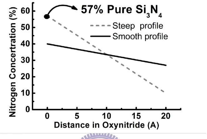
To investigate the impact of N-profile to gate tunneling current, two kinds of SiON
samples (“Sample-A” and “Sample-B”) with different N-profiles were fabricated. Sample-A
had a steeper N-profile than Sample-B, as illustrated in Fig. 3-1. The N-profile was measured
using high resolution angle-resolved XPS. To have a fair comparison, both thickness and
N-dosage were kept equal. The corresponding electrical data in terms of EOT, inversion gate
tunneling-current (Jg), and Jg-ratio (defined as Jg-A/Jg-B) are shown in the Fig. 3-2. Two key
observations were made from the experimental data: firstly, Sample-A is having a higher Jg
than Sample-B, for both n- and pMOSFET. Secondly, Jg-ratio (defined as Jg-A/Jg-B) is higher in
pMOSFET than nMOSFET, indicating pMOSFET has a higher sensitivity in Jg towards
N-profile change. A model, based on the change of tunneling probability, arising from
localized band bending, is proposed to explain these experimental data. This model was built
follows.
In this model, WKB approximation is adopted to calculate the change of tunneling
probability under various biasing conditions. The tunneling probability (Tt) could be
expressed by: T𝑡 = 𝑒𝑥𝑝 [−2 ∫ √2𝑚 ∗(𝑥) ℏ [𝜑𝑆𝑖𝑂𝑁(𝑥) − 𝐸]𝑑𝑥 𝑇𝑝ℎ𝑦 0 ] (1)
where Tt ≡ tunneling probability, υSiON≡ SiON/Si potential barrier and m*≡ carrier’s
effective mass and x≡distance into SiON, determined from Poly/SiON interface.
To solve Tt, two parameters: υSiON(x) and m*(x), under different biases must first be
extracted. To simplify the model, several assumptions were made in this model. Firstly, the
nitrogen concentration is assumed to vary linearly within the bulk of SiON. Secondly, the
bulk of SiON is assumed to consist of “n” number of very thin SiON strips, with uniformly
distributed nitrogen in each strip. Thirdly, the energy barrier height (υ), dielectric constant (ε)
and effective tunneling mass (m*) for SiON are assumed to vary linearly with nitrogen dosage
between oxide material constants and those for nitride, as reference to Philip A. et al.[27, 34]
Following that, the various input parameters could be simplified to:
x a1x a2 N (2) 57 N N ox SiN ox (3) 57 N N ox SiN ox (4) 57 ) ( * * * * N m m m N m ox SiN ox (5)
where a1and a2are constants, and we can obtain a variety of linear N profile shapes by
modifying those values. The N and NSiN are nitrogen concentrations (atom %) in the
oxynitride film and the pure nitride film, respectively. The other used constants are
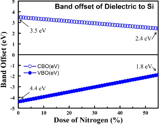
summarized in the Table 3- 1 and Fig. 3-3. Substituting these parameters [φ(x), ε(x) and m*(x)]
into the main expression in Eq. (1), we could simulate the tunneling probability through the
different potential barriers. Figure 3-4 and Figure 3-5 respectively shows the simulated
N-profiles and corresponding band diagram under a bias (VOX) of 0 V.
For VOX ≠ 0, Poisson’s equation shall be adopted to describe the non-homogeneous
change of dielectric constant within SiON:
0 dx x dV x dx d SiON (6)
Where VSiON(x) and ρ are representing the potential and free charge density within SiON,
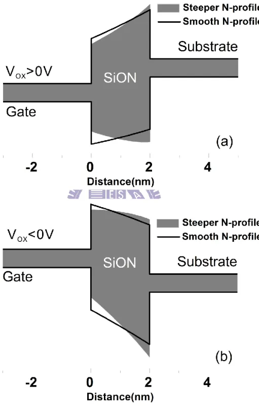
respectively. Solving for Poisson Equation, we are able to simulate the band diagram for
SiON with different N-profiles, as shown in Fig. 3-6. Therefore, the corresponding tunneling
probability nMOSFET under VOX > 0 V and for pMOSFET under VOX<0 V can be simulated.
To examine our model, the case of two SiON samples with different N-profiles is
considered, as depicted in Fig. 3-4. Both samples are having the equal nitrogen concentrations
and thickness. Under zero bias (i.e., VOX = 0V), the simulated energy band diagram are shown
in Fig. 3-5 and Fig. 3-6. The SiON sample with steeper N-profile exhibits a steeper
bending is steeper than that of CB. This is attributed to the greater VB offset (than CB offset)
difference comparing SiO2 to Si3N4, as shown in the Table 3- 1.
Under nonzero biasing (i.e., VOX 0), there will be an additional voltage drops across the
silicon oxinitride (VSiON). Hence, it is necessary to consider both υ(x) and VSiON(x) for
constructing the potential barrier, while simulating the energy band diagrams. Considering
minority carriers under operation mode (at low electric field),[35] the simulated tunneling
probability for electrons (in nMOSFET) under positive biasing, and holes (in pMOSFET)
under negative biasing are plotted in Fig. 3-7. These experimental results are also shown in
Fig. 3-8. These I-V curves in Fig. 3-8 are the average results of five devices for each kind of
samples. The gate current density (Jg) ratios of the steep profile to the smooth profile for
n/pMOSFETs are also presented. The range of gate bias for measuring Jg ratios is just shown
between -1.25 to -0.5V for pMOSFET and between 0.5 to 1.5 V for nMOSFET. The carrier
transport mechanism in the bias range can be attributed to the direct tunneling behavior,
which is verified by conduction processes fitting.[28]
According to simulated results, it shows that sample with steeper N-profile exhibits a
higher tunneling probability, valid for both n- and pMOSFETs. This result agrees well with
our experimental data in Fig. 3-8. On the other hand, defining the tunneling probability ratio
(TP-ratio) as TPsteep/TPsmooth, it is observed holes (in the pMOSFET) have a higher TP-ratio
higher JG increase. This is particularly true for pMOSFET because VB bending is more
sensitive to N-profile change than CB bending, as predicted by our model.
3.3 Effect of high tensile stress on ultrathin nitrided oxides
The introduction of strain into the channel region does not only enhance the mobility of
electrons and holes by altering the in-plane mass, it also changes the gate tunneling current by
altering the out-plane mass and SiO2/Si barrier height. However, the change of strain will
make a great impact on the gate tunneling current.[11] Previous articles have reported the
reduction of gate tunneling current by introducing the tensile strain in nMOSFET.[13, 16] In
the course of boosting nMOSFET mobility using SMT with high tensile strain, the gate
tunneling current was also found to be increased at the same time. This is particularly evident
when the channel is driven into accumulation mode. This observation is rather different from
previous reports. In this study, two possible factors will be investigated to analyze the
anomalously high gate tunneling currents. One is the strain-induced excessive lateral dopant
diffusion, and the other is the strain-induced polysilicon gate damage at the edges.
The nMOSFET used in this work was fabricated using state-of-the-art CMOS processes.
The device went through the gate dielectric, gate poly, spacer and source/drain (S/D)
formation.[36-38] The lightly-doped drain-source (LDD) and S/D regions were implanted
with arsenic and phosphorous, respectively. High tensile SMT film is then deposited and
Two NMOSFETs (sample-A and sample-B) with different strain level were compared to
investigate the effect of strain on gate tunneling current. Sample-A is having a higher tensile
strain than Sample-B. Keithely 4200 Semiconductor Characterization System and Agilent
4294 Precision Impedance Analyzer are the key instruments used to extract various device
parameters.
In Fig. 3-9 and Fig. 3-10, the electrical characteristics of nMOSFET devices show that
Sample-A (with higher tensile strain) has approximately 4% higher mobility than Sample-B
(with lower tensile strain). Figure 3-9 also shows that the sample with higher strain also
exhibits a higher drain leakage current (Id-off) at off states. This is particularly evident when
the device is biased at a linear mode (Vd=0.05V). Electrical measurement shows that the
higher Id-off is mainly contributed from the higher gate tunneling current.
Carrier separation measurement was performed to identify the source and the type of
carriers tunneling through the gate dielectric.[39] The gate tunneling current is plotted as a
function of gate bias (Vg) in Fig. 3-11.The measured gate current could be divided into two
distinctive regions. For the low Vg region, Sample-A exhibits a much higher Jg than Sample-B.
As Vg increases, the difference in Jg diminishes. Carrier-separation measurement shows
electron and hole tunneling currents dominate at a low and a high gate biasing regions, as
respectively shown in Fig. 3-12 and Fig. 3-13. At the low biasing region, the gate tunneling
tunneling current than Sample-B. This could be originated from the different tensile strain. It
has been reported that tensile strain from a SMT is huge at the gate edge.[16, 40] Therefore, it
is reasonable to deduce that the anomalously high gate tunneling current in Sample-A is a
result of higher tensile strain.
Figure 3-14 examines the gate tunneling current of nMOSFET devices with gate bias at
-0.75 V for various channel lengths. The results show that the gate tunneling current is a
function of channel length. As the channel length is decreased, the impact from strain
becomes more evident. The mechanical stress induced by SMT is not only originated from the
vertical compressive strain or restraining polysilicon gate from re-growth, it also comes from
the tensile strain experienced by the S/D regime (SMT). This explains the dependence to
channel length [41, 42]. In other words, the tensile strain experienced from SMT will be
increased with the reduction of channel length, resulting in the increased gate tunneling
current.
On the other hand, it is also observed that Sample-A is having approximately 9% higher
gate-to-S/D overlapping capacitance than Sample-B, as shown in the Fig. 3-15. Excessive
strain was reported to induce point defects, such as interstitials and vacancies in silicon. The
presence of these defects assists dopant diffusion. Hence, both the tensile and compressive
strain would influence the dopant diffusion behavior.[43] In our samples, the LDD was
lateral arsenic diffusion. This explains Sample-A is having a higher gate-to-S/D overlapping
capacitance. In addition, the change in overlapping capacitance increases gate tunneling
current at gate edge.
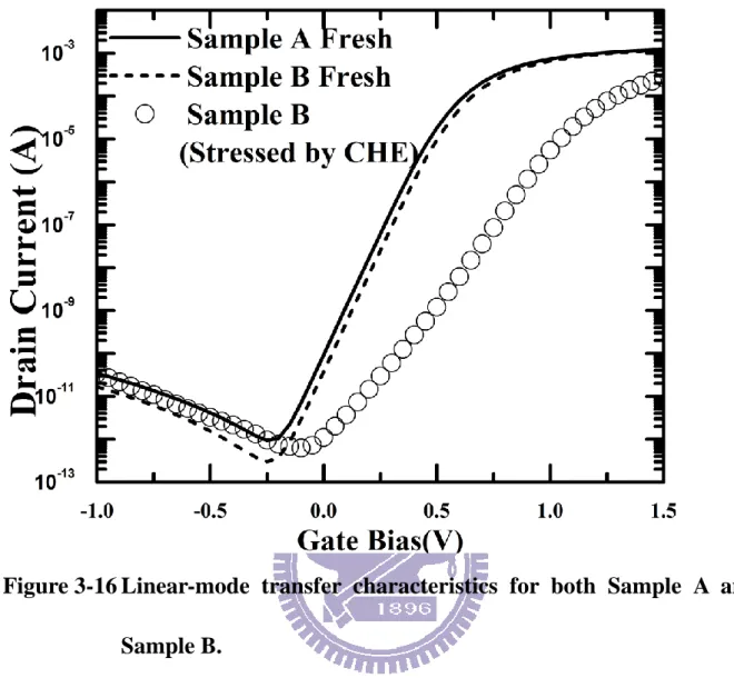
Figure 3-16 shows transfer characteristics of Sample-A and Sample-B in the linear mode,
at a drain voltage of 0.05V. The drain current of Sample-A is higher than that of Sample-B in
the off state. The threshold voltage of Sample-A is slightly lower than Sample-B. These
results could be attributed to the effects of strain-induced mobility increment and
strain-induced lateral LDD dopant diffusion, which shortens the effective channel length
further. In Fig. 3, Sample-B was also intentionally subjected to 1000 sec channel hot electron
(CHE) stress to create damage at the proximity of gate edge. Following the channel hot
electron stresses, threshold voltage shifts positively with degradation in sub-threshold swing.
During hot carrier stress, hot electrons were injected into the gate dielectric and create
interface traps.[12, 44] Compared with fresh Sample-A without stress, the stressed device
produces an increased off-state drain current (Id-off), indicating that Id-off increases when the
gate edge is damaged. This verifies our inference that an excessive tensile strain at gate edge
3.4 Summaries
In summary, we have proposed a model based on WKB that could well explain the gate
tunneling-current through thin SiON with different N-profile. The change in N-profile
influences the band shape of SiON, causing the change in tunneling probability. The SiON
film with steeper N-profile will exhibit a higher gate tunneling-current. Also, the phenomenon
is more apparent in pMOSFET than in nMOSFET. The higher sensitivity of VB bending
towards N-profile change explains why pMOSFET is showing a larger current increment than
nMOSFET.
This article shows that SMT boosts the electrical performance of nMOSFET, but the gain
was achieved at the expense of a higher off-state gate tunneling current. Carrier separation
measurement shows the increased gate tunneling current is originated from the higher
gate-to-S/D tunneling current, which worsens when channel length gets shorter. Excessive
strain degrades gate tunneling current via two approaches: (1) excessive LDD dopant
diffusion and (2) gate edge damage. This was verified from the higher gate-to-S/D
![Figure 1-4 Correlation of dielectric constant with band gap of candidate [8]](https://thumb-ap.123doks.com/thumbv2/9libinfo/8749638.205620/39.892.134.785.119.702/figure-correlation-dielectric-constant-band-gap-candidate.webp)
![Figure 2-4 The ionic product of water at high temperature and high pressure.[29]](https://thumb-ap.123doks.com/thumbv2/9libinfo/8749638.205620/49.892.127.809.624.906/figure-ionic-product-water-high-temperature-high-pressure.webp)