1
AnaloP and Mixed-Simal Circuits and Svstems
1.5V CMOS Bootstrapped Dynamic Logic Circuit Techniques (BDLCT)
Suitable(for Low-Voltage Deep-Submicron
CMOS VLS1)ifor
Implementing 482MHz Digital Quadrature Modulator and Adder
J.
H.
Lou,
J.
B.
Kuo
Rm.
338, Dept.
of Elec. Eng.
National Taiwan University
Roosevelt' Rd. Sec. 4, Taipei, Taiwan 106-17
Fax:886-2-363-6893, Phone:886-2-363-5251x338,Email:jbkuo@cc.ee.ntu.e~u.t~
Abstract
This paper reports 1 . W
CMOS
bootstrapped dynamic logic circuit techniques (BDLCT) suitable for low-voltage deep-submicron CMOS VLSI. Using BDLCT, the maxi- mum operating frequency of a digital quadrature modu- lator is 482MHz a t 51' and 68MHz at 1.5V. Compared t o the circuit without BDLCT, t h e 1Zbit delay time of in a16-bit adder with BDLCT is improved by 56% at 1.5V.
Summary
Introduction
For next-generation VLSI circuits using deep- submicron CMOS technology, low supply voltage is the trend. Designing CMOS circuits using low supply voltage is a challenge. Recently, a
1.5V
full-swing bootstrapped CMOS static driver circuit was reported [l]. To enhance the speed performance of ClLIOS dynamic logic circuits using low supply voltage is also important.A
theoretical concept of a 1.5V CMOS dynamic logic circuit using the bootstrapped technique was reported [2]. In this paper, BDLCT suitable for low-voltage deep-submicron CMOSVLSI- the bootstrapped dynamic logic circuits and all- N-logic true-single-phase bootstrapped dynamic logic cir- cuits have been used in an adder and a digital quadrature modulator.
1.5V
BDLCT
Fig. 1 shows the 1.5V CMOS bootstrapped dynamic logic circuit techniques (BDLCT) in terms of (a) the 1.5V bootstrapped dynamic logic (BDL) circuit and (b) the 1.5V all-E-logic true-single-phase (TSP) BDL circuit.
(a)
1.5V
BDLAs shown in Fig. l ( a ) , the BDL circuit is composed of the input stage and the bootstrapper stage. When the input t o the bootstrapper circuit
(Vdo)
is high, MPB is off andMN is on. Therefore, the output of it is pulled t o ground.
VI
is low, hence MP is on and&
is pull high toI,&.
The bootstrap device DIPC, which is made of a PMOS device with its source and drain tied together, stores an amount of ( V d d-
Iti.p()C,,,WL
charge. When the inputt o the bootstrapper ( v d o ) switches from high to low, MN
turns off and MPB turns on. Meanwhile,
VI
changes to high and M P turns off. Since the bootstrap device M P C turns off, the holes evacuated from MPC makeV6
go up to exceed Vdd- the internal voltage overshoot. Therefore,the output
(Vout)
will also go up t o surpass Vdd. Thevoltage overshoot at the output of the bootstrapper circuit enhances the driving capability of the next stage hence the speed performance can be improved.
(b) 1.5V
TSP BDL
As shown in Fig.l(b), the l.5V all-Y-logic true-single- phase (TSP) BDL circuits: the nl-block and the n2-block have been created. T h e nl-block is identical t o the BDL circuit except MCN1. When CK is low, M C N l is off and the output of nl-block keeps its previous state. When CK
is high, the function of the nl-block is the same as BDL. In a pipelined system using all-N-logic T S P BDL circuits, the nl-n2-nl-n2 arrangement is required. When the nl- blocks are in the precharge period, the n2-blocks are in the logic evaluation period. Therefore, the bootstrapped output of the nl-block may help drive the following n2- block. In the nZblock, when CK is high, MPD is off and the input N-logic is separated from Vdd. The v d p node is
predischarged t o ground since MND is on. The output of n2-block
Vout:!
keeps its previous state since both MCP2 and MN are off. When CK is low, MPD turns on and MND is off- the logic evaluation period. If all inputs toinput stage bootstrapper stage Vd, = 1.5v
'
Vd, = 1.5v N1 -block N2-
block V o u n -0 Manchester CLA SO COFig. 1: The l.5V CMOS bootstrapped dynamic logic cir- cuit techniques (BDLCT) (a) the 1.W BDL circuit and (b) the 1.5V all-N-logic true-single-phase (TSP) BDL cir- cuit (c) the l.5V adder circuit using the BDLCT (BDL circuit).
-
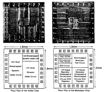
1.9mm-Floor Plan 01 the Adder Chip
,
I
i i ! l.Smm I iI
~Floor Plan of the Modulator Chip
Fig. 2: Die photos of the adder and modulator chips using BDLCT and without.
the n2-block are high, V d p is pulled high to v d d
-
&,(V&),where
V/;,(Vdp)
is the threshold voltage of the NMOS de- vice when its source voltage is v d p due to the body effectof the NMOS device. Therefore.
>IN
turns on and the output voltage Vout2 is pulled low. The switching speedof
Vout2
and the stability of the v d p level can be improvedby raising the ?$p level by- MFN and MFP. When
\IS
turns on. MFN also turns on, which pulls the node uolt- age V,, to ground. Thus,MFP
turns on and v d p is pulledhigh to K l d .
Experimental
Results
In order to show the effectiveness of BDLCT, a 1.3V adder circuit and a 1.3V digital quadrature modulator have been integrated using a standard 0.5pm CMOS tech- nology.
(a) 1.5V Adder
Fig. l ( c ) shows a 1.5V CMOS adder circuit using the Manchester carry look-ahead circuit with the BDL cir- cuit. Die photos of the test chips are shown in Fig. 2. Fig. 3 shows the measured transient waveforms in the 16- bit 1.5V
CMOS
adder circuit with the Manchester carry look-ahead circuit (a) with BDLCT at 1 5 V , (b) without BDLCT at 1.5V, (c) with BDLCT at 5V, (d) without BDLCT at 5V. With BDLCT, during the transient the pass transistor in the carry look-ahead circuit can turn on earlier. A t 1.5V. with BDLCT the 12-bit delay in the 16-bit adder circuit is 27.611s and without BDLCT. it iswith BDLCT without B D L M i 1.5V 1v T CK CK c3
-
c15 c3 cl 5 (a1Fig. 3: Measured transient waveforms of the 16-bit CMOS adders with and without BDLCT (BDL) a t 1.5V and 5V.
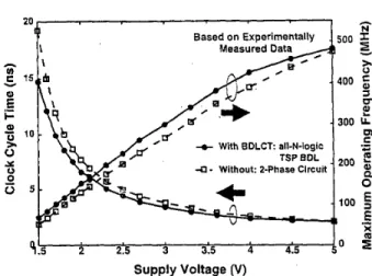
Decodar X Y c ' "out Based on Experimentally Measured Data 40 .535 without BDLCT Supply Voltage (V)
Fig. 4: Measured 12-bit delay time vs supply voltage in the 16-bit CMOS adder with and without BDLCT.
43.0511s. At 5V, with BDLCT it is 5.78ns and without BDLCT it is 7.111s. Fig.
4
shows the measured 12-bit delay time vs the supply voltage of the 16-bit adder carry look-ahead circuit with and without BDLCT. At5V,
with BDLCT the propagation delay improves about 10%. At1.5V,
withBDLCT
it improves 36%. Therefore, BDLCT is especially effective at low-voltage.(b) 1.5V Quadrature Modulator
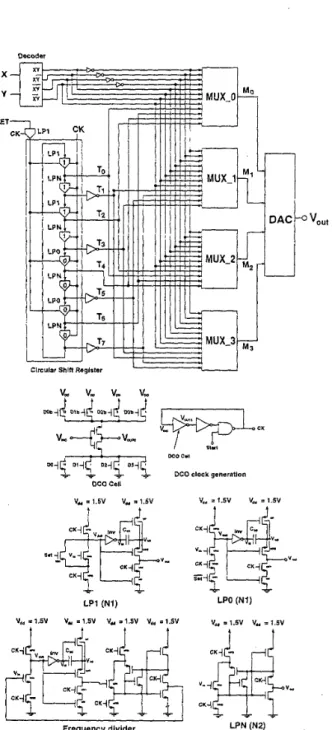
Fig. 5 shows the block diagram of a digital quadrature modulator [3]. It has an 8-stage circular shift register and 4 multiplexers to provide a four-bit digital output for representing a $level analog output. The 8-stage circu- lar shift register is used to generate a set of eight adja- cent outputs with various phases. The multiplexers are
DCO Cell V., = 1.5V V, = 1.5V
+ t
,
cK+rDco Cdl
DCO clock gsnsratlon
V . . = 1.5V Vu = 1 . W t t f LP1 (NI) 4-
c
LPO (NI) V,.l.SV V,=l.SV V..=l.5V V...l.SV V...l.SV v...1.5v t t t I I Frequency divider L P N (N2)Fig. 5: Block diagram of the 1.5V CMOS quadrature mod- ulator using BDLCT (all-N-logic TSP BDL).
”dd = I Di
F
FI Div?
withaul BDLCT OIP r e a . O P To T*Fig. 6: Measured transient n-aveform of the CMOS quadrature modulator with and without BDLCT at 1.5V and 5V.
used to select four appropriate outputs from the eight shift register outputs depending on the input baseband signals
X
andY.
In
the circular shift registers, ‘preset- to-1’ (LPl), ‘preset-to-0’ (LPO),
and ‘no-preset’ (LPN) latches based on all-X-logicTSP
BDL circuits have been designed. In order to maximize the operation frequency, a digital controlled oscillator (DCO) is used t o generatean on-chip clock. Fig. 6 shows the measured transient waveforms of the digital quadrature modulator using the all-N-logic TSP BDL circuits. (a) with BDLCT a t 1.5V, (b) without BDLCT at 1.5V, (c) with BDLCT at 5V, (d) without BDLCT a t 5V. At 1.5V, with BDLCT the modulator works at a minimum clock cyle time of 15.9ns and without BDLCT it works at 20.211s. At 5V, with BDLCT it works at a minimum clock cycle time of 2.lns and without BDLCT it works at 2.1511s. With BDLCT, i t works at a faster speed. Fig. 7 shows the clock cycle time and the maximum operating frequency vs the sup- ply voltage of the digital quadrature modulator with and without BDLCT. At 5V, the digital quadrature modula- tor works at a ma-ximum operating frequency of close to
5OOMHz. With BDLCT, at 5V, t h e maximum operating frequency is slightly higher. As the supply voltage de- creases, the maximum operating frequency decreases.
At
1.5Vl with BDLCT its maximum operating frequency is 68MH2, which is 27% faster than t h a t without BDLCT.
Discussion
Supply Voltage (V)
Fig. 7 : Measured clock cycle time and maximum operat- ing frequency vs supply voltage of the digital quadrature modulator with and without BDLCT.
of 2 and a fan-out of 4, the 1V
CMOS
BDL circuit has a speed enhancement of1.8
times.Acknowledgments
The author would like t o thank
S.
C. Lin, E(. W.Su,
and Y. M. Huang for their helps on meaurements and graphics.
References
J. H. Lou and J. B. Kuo,
“A 1.5V
Full-Swing Boot- strapped CMOS Large Capacitive-Load Driver Cir- cuit Suitable for Low-Voltage CMOS VLSI”,
IEEE
J . Solid-State Circuits, Vol. 32, No. 1, pp. 119-121, Jan. 1997.
J.
H.
Lou and J. B. Kuo., “1.5V CMOS and BiCMOS Bootstrapped Dynamic Logic (BDL) Circuits using aCMOS
Bootstrapper Circuit”, Tech. Digest of Symp.VLSI
TSA, Taipei, June 1997.P. F.
Lin,J. H.
Lou, andJ.
B. Kuo,“A
CMOS
Quadrature Modulator for Wireless Communication IC,”
IEEE
Trans. Circuits and Systems-I, Vol.44,
No. 6 , pp. 559-561, June 1997.
The BDLCT reported in this paper is especially useful for low-voltage application. From experimental measure- ment, it can work at a supply voltage of 1.3V using the conventional