國立高雄大學應用物理學系研究所
碩士論文
低壓化學氣相沉積在玻璃基板上成長厚度壓力與參雜濃度
為變數之摻硼氧化鋅薄膜之特徵與分析
Characterizations and analyses of thickness-, pressure-, and
doping-dependent ZnO:B films grown on glass substrates by a
low-pressure chemical vapor deposition
研究生:李偉銘 撰
指導教授:馮世維 博士
蔡進譯 博士
致謝
能順利完成這兩年的研究所學業與畢業論文,家人朋友師長的支持是不可或缺的, 首先要感謝的是我的父母,不論在何時他們總是給予我最大的支持與鼓勵,讓我求學過 程遇到艱難也能夠有信心的去面對。再來是感謝我的指導教授馮世維博士以及共同指導 教授蔡進譯博士,馮老師對於研究上的熱誠以及處事的認真態度影響我極深,特別是對 於研究上的熱誠以及處事細心認真的態度實在值得我們學習;蔡老師在我研究上遇到問 題時,給我許多啟發與建議,讓我收穫良多。接著,要感謝的就是陳建勳博士與賴志明 博士,在我口試時提出我在研究上有所不足的地方,給予我許多的意見及幫助。最後, 要感謝研究所同學盈翔、博勛、俊毅、威佐、瓊毅,在碩士生活中互相幫助與分憂,讓 我的求學生活更加充實與快樂;也感謝少強學弟,平時幫我分擔雜事,使我能夠順利走 完碩士求學生涯。 李偉銘 敬上 2018/08低壓化學氣相沉積在玻璃基板上成長厚度壓力與參雜濃度
為變數之摻硼氧化鋅薄膜之特徵與分析
指導教授:馮世維 博士 蔡進譯 博士 國立高雄大學應用物理學系研究所 學生:李偉銘 國立高雄大學應用物理學系研究所 摘要 在第一章,我們透過低壓化學氣相沉積在玻璃基板上成長不同厚度的摻硼氧化鋅 (ZnO:B)薄膜。我們進行陰極射線(CL)、拉曼光譜、掃描式電子顯微鏡(SEM)、原 子力顯微鏡(AFM)和X射線衍射(XRD)分析等實驗。從X射線繞射數據分析發現, 在低摻雜中,最薄摻硼氧化鋅樣品(002)的晶粒百分比大於(100)和(110),當厚度增加, (110)的晶粒百分比逐漸增加到最大,最薄的樣品幾乎生長具有或不具有錐形尖端結構 的(002)六角形圓柱體;中等和較厚的樣品特別有利於(110)脊狀晶粒結構的生長。另一 方面,從X射線繞射數據分析發現,高摻雜摻硼氧化鋅薄膜特別有利於(110)脊狀晶粒結 構的生長。這些結果和陰極射線、拉曼光譜、掃描式電子顯微鏡、和原子力顯微鏡所觀 測出的情況一致。 在二章,我們將不同壓力的摻硼氧化鋅(壓力分別為0.4和0.6 torr)和不同摻雜濃度的 摻硼氧化鋅(摻雜濃度分別為1和3 sccm)薄膜,生長在玻璃基板。我們進行陰極射線(CL), 拉曼光譜,掃描電子顯微鏡(SEM),原子力顯微鏡(AFM)和X射線繞射(XRD)分 析等實驗。從X射線繞射結果發現,摻硼氧化鋅生長傾向於(110)晶面,且不同壓力和摻 雜濃度的摻硼氧化鋅,厚度增加,所受平均應力減少,且平均晶粒尺寸增加。在玻璃基 板上壓力0.4torr的摻硼氧化鋅晶粒的平均尺寸比0.6torr的摻硼氧化鋅大;壓力0.4torrt的0.4torr摻硼氧化鋅穿透率大。另一方面,摻雜濃度1sccm摻硼氧化鋅晶粒的平均尺寸比摻 雜濃度3sccm摻硼氧化鋅大;而摻雜濃度1sccm摻硼氧化鋅晶粒的平均應力比摻雜濃度 1sccm摻硼氧化鋅小。厚摻雜濃度3sccm摻硼氧化鋅的穿透率比摻雜濃度1sccm摻硼氧化 鋅的穿透率大。這些結果和陰極射線、拉曼光譜、掃描式電子顯微鏡、和原子力顯微鏡 所觀測出的情況一致。 關鍵詞:氧化鋅,透明導電氧化物,矽,太陽能電池,X射線衍射,掃描電子顯微鏡, 原子力顯微鏡,拉曼光譜,陰極射線發光。
Characterizations and analyses of thickness-, pressure-,
and doping-dependent ZnO:B films grown on glass
substrates by a low-pressure chemical vapor deposition
Advisor: Dr. Shih-Wei Feng Dr. Chin-Yi Tsai Institute of Applied Physics National University of Kaohsiung
Student: Lee, Wei-Ming Institute of Applied Physics National University of Kaohsiung
ABSTRACT
In the first chapter, thickness-dependent boron-doped zinc oxides (ZnO:B) thin films are grown on the glass substrates by a low-pressure chemical vapor deposition (LPCVD). They are characterized and analyzed by cathode luminescence (CL), Raman spectroscopy, scanning electron microscope (SEM), atomic force microscope (AFM) and X-ray diffraction (XRD) measurements. For the thinnest low-doping ZnO:B sample, the grain percentage of ZnO(002) is larger than those of the ZnO(110) and ZnO(100). As the thickness increases, the grain percentage of ZnO(110) is the largest and increases gradually. The thinnest low-doping sample almost produces ZnO(002) hexagonal cylinders with or without the pyramidal-tip structures, while the medium and thicker low-doping samples particularly favor the growth of ZnO(110) ridge-like grain structures. On the other hand, the XRD result shows that the high-doping ZnO:B films particularly favor the growth of ZnO(110) ridge-like grain structures. These XRD results are shown to strongly agree with the SEM, AFM, CL, and transmittance measurements as well.
0.6 torr) and doping-dependent boron-doped zinc oxides (ZnO:B) (1 and 3 sccms) thin films are grown on glass substrates. They are characterized and analyzed by cathode luminescence (CL), Raman spectroscopy, scanning electron microscope (SEM), atomic force microscope (AFM) and X-ray diffraction (XRD) measurements. The results show that BZO grains with the (110) crystal orientation are most favored to grow on glass substrates. The XRD data also show that the average grain sizes of pressure-dependent BZO grown on glass substrates decrease due to the increases of their average strains. The average size of ZnO0.4 grains on the glass substrate
is slightly larger than that on ZnO0.6; whereas, the average strains on the ZnO0.4 are slightly
smaller than that on the ZnO0.6. The transmittance spectra of ZnO0.6 is larger than that on the
ZnO0.4. On the other hand, the average size of BZO1 grains on the glass substrate is slightly
larger than that on BZO3 grains on the glass substrate; whereas, the average strains on the BZO1
are slightly smaller than that on the BZO3. The average transmittance spectra of BZO3 is
slightly larger than that on the BZO1. These results strongly agree the measurements from the
CL, Raman, SEM, and AFM as well.
Keywords: ZnO, Transparent conducting oxide, Silicon, Solar cells, X-ray diffraction,
Scanning electron microscope, Atomic force microscope, Raman spectroscopy, Cathode luminescence
Contents
中文摘要
……….………I
Abstract………...III
Contents………V
Table Captions……….VIII
Figure Captions………...IX
Chapter 1 Characterizations and analyses of the low- and high-doping
ZnO:B films grown on glass substrates by a low-pressure chemical vapor
deposition………...………...….1
1.1 Introduction ………...1 1.2 Motivation and investigation procedures………...….……...3 1.3 Sample structures and growth conditions of low-doping ZnO:B grown on glass substrates……...………...………...3 1.4 Characterizations and analyses of low-doping ZnO:B grown on glass substrates……….……....…...4 1.4.1 X-Ray diffraction and lattice strain………...………..4 1.4.2 Scanning electron microscope (SEM), cathodo-luminescence (CL), and atomic force microscopy (AFM) studies……...……….………...…..5 1.4.3 Estimation of strain by Raman scattering measurement………..……….7 1.5 Sample structures and growth conditions of high-doping ZnO:B grown on glass substrates……...………...………...8 1.6 Characterizations and analyses of high-doping ZnO:B grown on glass substrates……….……....…...9 1.6.1 X-Ray diffraction and lattice strain………...………..9 1.6.2 Scanning electron microscope (SEM), cathodo-luminescence (CL), and atomic force
microscopy (AFM) studies……...……….………...…10
1.6.3 Estimation of strain by Raman scattering measurement………...…..11
1.7 Discussion and Summary..………...12
References...14
Chapter 2 Characterizations and analyses of the pressure- and
doping-dependent ZnO:B films grown on glass substrates by a low-pressure
chemical vapor deposition………...….37
2.1 Introduction ………...37
2.2 Motivation and investigation procedures………...….…….37
2.3 Sample structures and growth conditions of the pressure-dependent ZnO:B grown on glass substrates……...………...……….38
2.4 Characterizations and analyses of the pressure-dependent ZnO:B grown on glass substrates………...….38
2.4.1 X-Ray diffraction and lattice strain………...……….38
2.4.2 Scanning electron microscope (SEM), cathodo-luminescence (CL), and atomic force microscopy (AFM) studies……...………....…40
2.4.3 Estimation of strain by Raman scattering measurement……….……41
2.5 Sample structures and growth conditions of the doping-dependent ZnO:B grown on glass substrates……...………...……….42
2.6 Characterizations and analyses of the doping-dependent ZnO:B grown on glass substrates……….……....….42
2.6.1 X-Ray diffraction and lattice strain………...………43
2.6.2 Scanning electron microscope (SEM), cathodo-luminescence (CL), and atomic force microscopy (AFM) studies……...……….………...…44
2.7 Discussion and Summary..………...45 References...47
Table Captions
Table 1.1 Peak intensities, FWHMs, and integrated intensities of XRD peaks and the corresponding grain percentages, average grain sizes, and average strains of the low-doping BZO20, BZO40, BZO50, BZO60, and BZO70 samples……….…..16 Table 1.2 Thickness, main grain, surface morphology, RQ of AFM, grain size (D), lattice constants a and c, CL intensity, and energy gap (Eg) of the low-doping BZO20, BZO40, BZO50, BZO60, and BZO70 samples……….………...17 Table 1.3 Peak intensities, FWHMs, and integrated intensities of XRD peaks and corresponding grain percentages, average grain sizes, and average strains of the high-doping BZO20, BZO40, BZO60, and BZO70 samples……….... ………...18 Table 1.4 Thickness, main grain, surface morphology, RQ of AFM, grain size (D), lattice constants a and c, CL intensity, and energy gap (Eg) of the high-doping BZO20, BZO40, BZO60, and BZO70 samples………...……….…....19 Table 2.1 Peak intensities, FWHMs, and integrated intensities of XRD peaks and the corresponding grain percentages, average grain sizes, and average strains of the BZO0.4 and
BZO0.6 samples………..………...48
Table 2.2 Thickness, main grain, surface morphology, RQ of AFM, grain size (D), strain, lattice constants a and c, CL intensity, and energy gap (Eg) of the BZO0.4 and BZO0.6
samples………... ……….49 Table 2.3 Peak intensities, FWHMs, and integrated intensities of XRD peaks and corresponding grain percentages, average grain sizes, and average strains of the BZO1 and BZO3
sample.……....………..50 Table 2.4 Thickness, main grain, surface morphology, RQ of AFM, grain size (D), lattice constants a and c, CL intensity, and energy gap (Eg) of the BZO1 and BZO3
Figure Captions
Figure 1.1 The mineral wurtzite is a crystal structure for various binary compounds…………..……….20 Figure 1.2 SEM images of PET/ZnO thin films at different deposition temperatures: (a) 383 K, Rs ~ 10 k Ω at d ~ 560 nm, (b) 398 K, Rs ~ 2 k Ω at d ~ 720 nm, (c) 423 K, Rs ~ 250 Ω at d ~ 1080 nm, and (d) 428 K, Rs ~ 300 Ω at d ~ 1250 nm………..………...20 Figure 1.3 Experimental flow chart of this chapter…..………..……...21 Figure 1.4 Structures of the low-doping BZO20, BZO40, BZO50, BZO60, and BZO70 samples grown on glass substrates. 20, 40, 50, 60, and 70 mean growth times in minutes with corresponding to thicknesses 346.9, 950.5, 1077.2, 1316.8, and 1653.4 nm, respectively…...21 Figure 1.5 (a)XRD and (b)grain percentages obtained from XRD peaks of the low-doping BZO20, BZO40, BZO50, BZO60, and BZO70 samples………...22 Figure 1.6 (a) Peak intensities, (b) FWHMs, and (c) grain percentages of diffraction peaks ZnO(100), ZnO(002), and ZnO(110) for the low-doping BZO20, BZO40, BZO50, BZO60, and BZO70 samples………..………..23 Figure 1.7 (a) Grain size, (b) strains obtained from XRD peaks, and (c) averaged grain size versus XRD strain of the low-doping BZO20, BZO40, BZO50, BZO60, and BZO70 samples……….………24 Figure 1.8 (a) SEM and (b) CL experimental setups in a JEOL SEM system (model JSM 7000F)………..25 Figure 1.9 Experimental setup of AFM measurement………...25 Figure 1.10 SEM images of the low-doping (a) BZO20, (b) BZO40, (c) BZO50, (d) BZO60, and (e) BZO70 samples………...26 Figure 1.11 ZnO grown on glass substrates. (a) For ZnO(100), a polygon structure for the c-axis growth parallel to the substrate; (b) For ZnO(110), the ZnO grains will reveal ridge-like
pyramidal tip; (d) For ZnO(101), the ZnO grains mainly form the pyramidal tip without the hexagonal cylinder………26 Figure 1.12 AFM images (5 μm × 5 μm) of the low-doping (a) BZO20 (RQ 14.967nm), (b) BZO40 (RQ 34.555nm), (c) BZO50 (RQ 42.875nm), (d) BZO60 (RQ 55.862nm), and (e) BZO70 (RQ 60.245nm) samples. Surface roughness of each sample, Rq, is shown in the parentheses………...27 Figure 1.13 CL spectra of the low-doping (a) BZO20, (b) BZO40, (c) BZO50, (d) BZO60, and (e) BZO70 samples with the excitations of 16, 18, and 20kV electron voltages at room temperature……….………..28 Figure 1.14 Experimental setup of Jobin Yvon-Horiba Micro-Raman system (model T64000)……….………...29 Figure 1.15 Raman spectra of the low-doping BZO20, BZO40, BZO50, BZO60, and BZO70 samples……….………29 Figure 1.16 Transmittance spectra of the low-doping BZO20, BZO40, BZO50, BZO60, and BZO70 samples…..………..30 Figure 1.17 Structures of the high-doping BZO20, BZO40, BZO60, and BZO70 samples grown on glass substrates. 20, 40, 60, and 70 mean growth times in minutes with corresponding to thickness 391.9, 991.3, 1397.1, and 1664.1 nm, respectively…..………..30 Figure 1.18 (a)XRD and (b)grain percentages obtained from XRD peaks of the high-doping BZO20, BZO40, BZO60, and BZO70 samples………....31 Figure 1.19 (a) Peak intensities, (b) FWHMs, and (c) grain percentages of diffraction peaks ZnO(100), ZnO(002), and ZnO(110) for the high-doping BZO20, BZO40, BZO60, and BZO70 samples……….……….…...32 Figure 1.20 (a) Grain size, (b) strain obtained from XRD peaks, and (c) averaged grain size versus XRD strain of the high-doping BZO20, BZO40, BZO60, and BZO70 samples………33 Figure 1.21 SEM images of the high-doping (a) BZO20, (b) BZO40, (c) BZO60, and (d)
BZO70 samples...………....34 Figure 1.22 AFM images (5 μm × 5 μm) of the high-doping (a) BZO20 (RQ 9.109nm), (b) BZO40 (RQ 13.960nm), (c) BZO60 (RQ 22.556nm), and (d) BZO70 (RQ 28.440nm) samples. Surface roughness of each sample, Rq, is shown in the parentheses………..34 Figure 1.23 CL spectra of the high-doping (a) BZO20, (b) BZO40, (c) BZO60, and (d) BZO70 samples with the excitations of 16, 18, and 20kV electron voltages at room temperature….…35 Figure 1.24 Raman spectra of the high-doping BZO20, BZO40, BZO60, and BZO70 samples……….……....36 Figure 1.25 Transmittance spectra of the high-doping BZO20, BZO40, BZO60, and BZO70 samples……… 36 Figure 2.1 Feature size, haze, film thickness, and sheet resistance as a function of diborane flow……….………..………52 Figure 2.2 Experimental flow chart of this chapter……...………....52 Figure 2.3 Structures of the BZO0.4 and BZO0.6 samples grown on glass substrates. 0.4 and 0.6
mean growth pressures in torr with corresponding thicknesses 1,209 and 1,013 nm, respectively……….………..………53 Figure 2.4 (a)XRD and (b)grain percentages obtained from XRD peaks of the BZO0.4 and
BZO0.6 samples……….………..………..53
Figure 2.5 (a) Peak intensities, (b) FWHMs, and (c) grain percentages of diffraction peaks ZnO(100), ZnO(002), and ZnO(110) for the BZO0.4 and BZO0.6 samples………..…………..54
Figure 2.6 (a) Grain size, (b) strains obtained from XRD peaks, and (c) averaged grain size versus XRD strain of the BZO0.4 and BZO0.6 samples………..………55
Figure 2.7 SEM images of the (a) BZO0.4 and (b) BZO0.6 samples……..……...….…………56
Figure 2.8 ZnO grown on glass substrates. (a) For ZnO(100), a polygon structure for the c-axis growth parallel to the substrate; (b) For ZnO(110), the ZnO grains will reveal ridge-like
pyramidal tip; (d) For ZnO(101), the ZnO grains mainly form the pyramidal tip without the hexagonal cylinder………...……….56 Figure 2.9 AFM images (5 μm × 5 μm) of the (a) BZO0.4 (RQ 24.092nm) and (b) BZO0.6 (RQ
15.813nm) samples. Surface roughness of each sample, Rq, is shown in the parentheses…….57 Figure 2.10 CL spectra of the (a) BZO0.4 and (b) BZO0.6 samples with the excitations of 16, 18,
and 20kV electron voltages at room temperature……….………..……….…………..57 Figure 2.11 Raman spectra of the BZO0.4 and BZO0.6 samples….………...58
Figure 2.12 Lattice constants a and c of the BZO0.4 and BZO0.6 samples. For strain-free ZnO, a=3.25Å and c=5.204Å ………...……….…….58
Figure 2.13 Transmittance spectra of the BZO0.4 and BZO0.6 samples….…………....………59
Figure 2.14 Structures of the BZO1 and BZO3 samples grown on glass substrates. 1 and 3 mean
doping concentration with corresponding thicknesses 1,589 and 1,563, respectively……..…59 Figure 2.15 (a)XRD and (b)grain percentages obtained from XRD peaks of the BZO1 and BZO3
samples……….…60 Figure 2.16 (a) Peak intensities, (b) FWHMs, and (c) Grain percentages of diffraction peaks ZnO(100), ZnO(002), and ZnO(110) for the BZO1 and BZO3 samples..……….…61
Figure 2.17 (a) Grain size, (b) strain obtained from XRD peaks, and (c) averaged grain size versus XRD strain of the BZO1 and BZO3 samples………..……..…………...62
Figure 2.18 SEM images of the (a) BZO1 and (b) BZO3 samples……….63
Figure 2.19 AFM images (5 μm × 5 μm) of samples (a) BZO1 (RQ 25.856nm) and (b) BZO3
(RQ 19.386nm). Surface roughness of each sample, Rq, is shown in the parentheses……….63 Figure 2.20 Raman spectra of the BZO1 and BZO3 samples………64
Figure 2.21 Lattice constants a and c of the BZO1 and BZO3. For strain free ZnO, a=3.25Å and c=5.204Å samples………64
Chapter 1 Characterizations and analyses of the low- and high-doping
ZnO:B films grown on glass substrates by a low-pressure chemical vapor
deposition
1.1 Introduction
In recent years, ZnO has received enormous interest [1], because it has various superior properties, such as wide direct band gap of 3.3 eV at room temperature, large exciton binding energy of about 60 meV, and high optical transparency in the visible range [2]. ZnO is a self-activated crystal of hexagonal wurtzite structure with lattice constants a=3.25 Å and c=5.20 Å . Besides, ZnO has notable electrical properties including high electron mobility, breakdown strength, and electron drift velocity. Some physical properties, such as resistance to mechanical stress and high melting temperature, make ZnO promising for the fabrication of long lifetime devices. ZnO has been extensively studied for its promising applications in solar cells, transducers, varistors, optical waveguides, and gas sensors [3].
When applied in solar cells, TCOs could increase the solar cell’s photocurrent and efficiency and show higher haze for better light-trapping, while maintaining high electrical conductivity. Indium tin oxide (ITO), one of the most important TCO materials, has been well known for excellent transparent electrodes with a high optical transparency in the visible range and a high electrical conductivity for applications in displays, light-emission devices, solar-heating mirrors, and solar cells and modules [4-6]. Despite the excellent performance of ITO, numerous research efforts are being conducted to find other low-cost TCOs to replace or partially replace ITO due to the high cost and limited supply of its In content.
ZnO grown by a low pressure chemical vapor deposition (LPCVD) has been shown to be a good candidate as TCO for thin-film silicon solar cells. This is not only because of its high transparency over the visible and near-infrared (NIR) range, and of its electrical resistivity
that can be lowered down to 1103Ωcm, but also because of its capability to scatter efficiently the light that enters into the solar cell. The transparent and conducting features of ZnO thin films can successfully act as metal contacts while eliminate the blocking of the incident sunlight from the metals [1]. Since the surface on the ZnO thin film will form textures due to the formation of granular ZnO grains, these textures will function as a light-trapping structure. ZnO can increase the light-scattering capability by its textured surface and thus improve the solar cell performance. This scattering effect enhances the optical path inside the solar cell, and increases probability to be absorbed by the cell and the photo-generated current. As a result, for thin film solar cells, the ZnO not only serve the function as a TCO, but also a light-trapping structure.
Fig. 1.1 shows Zinc oxide crystallizes in two main forms, hexagonal wurtzite and cubic zincblende [7]. The wurtzite structure is most stable at ambient conditions and thus most common. The zincblende form can be stabilized by growing ZnO on substrates with cubic lattice structure. In both cases, the zinc and oxide centers are tetrahedral, the most characteristic geometry for Zn(II). ZnO converts to the rocksalt motif at relatively high pressures about 10 GPa.[8] Hexagonal and zincblende polymorphs have no inversion symmetry (reflection of a crystal relative to any given point does not transform it into itself). This and other lattice symmetry properties result in piezoelectricity of the hexagonal and zincblende ZnO, and pyroelectricity of hexagonal ZnO.
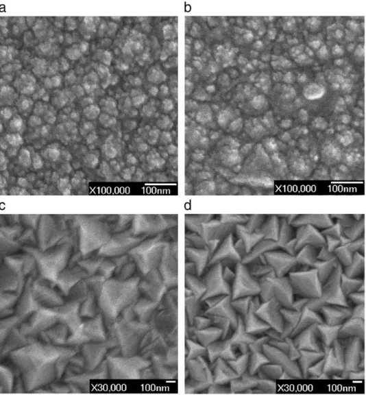
Fig. 1.2 shows the corresponding SEM images of PET/ZnO thin films. From the SEM images, we can see that the ZnO thin film prepared at low deposition temperature of 383 K exhibits a smooth surface with crystal grain size of about 30-80 nm. When the deposition temperature is increased to 398 K, the surface morphology of the ZnO thin films is rough with a mixture of some sphere-like and irregular structures. With the deposition temperature further increasing to 423 K and 428 K, sphere-like structures disappear and the crystal grain size increases up to ~300-500 nm with typical pyramid shape structure. In addition, thin film
thicknesses (d) gradually increase from ~560 nm to ~1250 nm as the deposition temperatures increase from 383 K to 428 K. The lowest sheet resistance, Rs~ 250 Ω, was obtained at the
deposition temperature of 423 K [9].
1.2 Motivation and investigation procedures
In this chapter, we investigate the low- and high-doping ZnO:B films grown on glass substrates with different film thicknesses by a LPCVD.
Fig. 1.3 shows the experimental procedures of this study. The growth methods and conditions of ZnO:B thin films on glass substrates will be described in the section 1.3. The surface morphologies of samples are measured by the atomic force microscopy (AFM) measurement and the scanning electron microscope (SEM). The film quality and its optical properties of the samples are studied by the cathodoluminescence (CL). The crystallization of ZnO grains and their substrates and properties are determined by X-ray diffraction (XRD) measurements. The strains of ZnO:B grains are analyzed by Raman scattering measurement. Analyzing the results of these measurements, we will discuss the characteristics and properties of ZnO:B thin flims grown on glass substrates with different film thicknesses. The experimental results and their theoretical explanations will be discussed in the Section 1.4. A brief conclusion will be summarized in the Section 1.7.
1.3 Sample structures and growth conditions of the low-doping ZnO:B films grown on glass substrates
Fig. 1.4 shows the sample structures of the low-doping ZnO:B films grown on glass substrates by a LPCVD with different film thicknesses. Glass substrates are prepared and cut into 22cm2 pieces. The ZnO:B films with the thickness of 0.306, 0.95, 1.077, 1.316 and 1.653 μm were deposited on glass substrates, (denoted as the sample BZO20, BZO40, BZO50,
during deposition is 0.6 torr. The deposition times for the BZO(0.306μm) to BZO(1.653μm) samples are 20 to 70 mins, respectively. Diethylzinc (DEZ) and water (H2O) vapors carried by
argon gas were used as precursors, and their flows were set to 500 and 550 sccm, respectively. The boron doping is accomplished by controlling the flow rate of B2H6 to 1 sccm.
1.4 Characterizations and analyses of the low-doping ZnO:B films grown on glass substrates
1.4.1 X-Ray diffraction and lattice strain
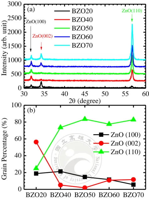
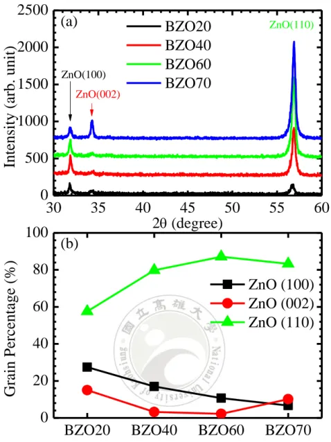
The samples are analyzed by using the XRD. The results are shown in Fig. 1.5(a). There are three main diffraction peaks from the crystalline ZnO:B grains: (100), (002), and (110) peaks, while the rest of the diffraction peaks are barely noticeable and thus will be ignored in the following discussion. Generally, the percentages of grains associated with different peaks are proportional to their correspondent XRD integrated intensities. As a result, the percentages of (100), (002), and (110) ZnO:B grains obtained from XRD data are shown in Fig. 1.5(b). The peak and integrated intensities, and the full width at half maximum (FWHM) of the (100), (002), and (110) peaks associated with three different crystalline orientations of ZnO:B grains are listed in the Table 1.1. Lattice constants a and c obtained from the XRD peaks of the BZO20, BZO40, BZO50, BZO60, and BZO70samples are shown in Table 1.2.
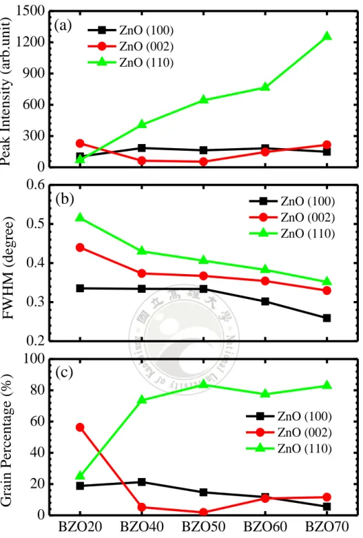
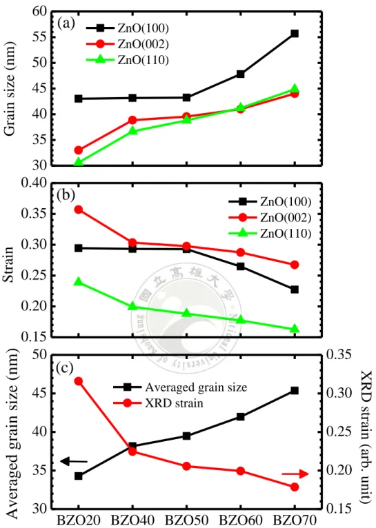
Fig. 1.6 shows the peak intensities, FWHMs, and grain percentages of the (100), (002), and (110) XRD peaks of the BZO20, BZO40, BZO50, BZO60, and BZO70 samples. In
addition, Fig. 1.7 shows the grain sizes, strains, and averaged grain size obtained from (100), (002), and (110) XRD peaks of the five samples. The ZnO:B grain sizes are analyzed as follows.
The ZnO:B grains on glass substrates have three major crystalline orientations: (100), (002), and (110). Their grain size, D, can be calculated from the following formula [10]
cos hkl D
where
hkl,
,
, and
are the FWHM, shape factor (usually 0.9), wavelength, anddiffraction angle of X-rays, respectively. As a result, the average grain sizes associated with different peaks can be calculated by using this formula. The calculated results are shown Table 1.1. The average grain size of the BZO70 sample are larger than that of the BZO20 sample.
The XRD data can be analyzed to obtain not only the percentages of different grain crystal orientations, but also the strains associated with them. The strains associated with the diffraction peaks can be calculated by the [10]
t a n 4 h k l
where
hkl
FWHM
, and
is x-ray diffraction. The strains on BZO70 are smaller thanthose on BZO20. From the results of the XRD, the average grain sizes of the low-doping ZnO:B films decrease due to the increases of their average strains.
1.4.2 Scanning electron microscope (SEM), cathodo-luminescence (CL), and atomic force microscopy (AFM) studies
In order to investigate the relation between optical properties and microstructures of ZnO:B thin films grown on glass substrates, scanning electron microscope (SEM) and cathodoluminescence (CL) measurements were conducted at the same spots of the samples. As shown in Fig. 1.8, SEM and CL images were acquired with a Gatan monoCL3 spectrometer in a JEOL SEM system (model JSM 7000F) under room temperature. The excitation electron voltages for CL measurement range from 16 to 20 kV.
To study the surface morphology of the BZO20, BZO40, BZO50, BZO60, and BZO70 samples. AFM measurement was conducted as well. Fig. 1.9 shows the experimental setup
of the AFM measurement. The AFM images were acquired with XE-70 control electronics under non-contact mode.
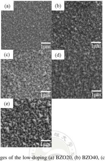
The surface structures from the results of the SEM are shown in the Fig. 1.10. As schematically illustrated in Fig. 1.11, the ZnO(100) grains will form a polygon structure with the c-axis parallel to the substrate surface. On the other hand, the ZnO(002) grains will form hexagonal cylinder with or without the pyramidal tip. In addition, the ZnO(110) grains will certainly reveal ridge-like structures to the surface. The SEM images show that ZnO grains on glass substrate have many ridge-like as well as pyramid-like structures. As a result, it is very difficult to estimate the percentage of these two different structures purely from the SEM images.
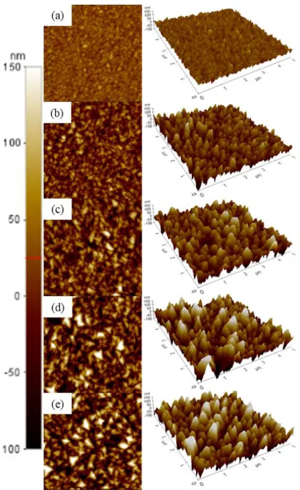
Fig. 1.12 shows the AFM images of the 5 μm × 5 μm samples of (a) BZO20 (Rq 14.967nm), (b) BZO40 (Rq 34.555nm), (c) BZO50 (Rq 42.875nm), (d) BZO60 (Rq 55.862nm), and (e) BZO70 (Rq 60.245nm). Surface roughness of each sample, Rq, is shown in the parentheses. However, from the AFM images, the surface roughness of the BZO70 is much sharper than that BZO20. Therefore, from the results of the AFM images, it can be conjectured that the BZO70 have more ridge-like structures than the hexagonal cylinder ones. On the contrary, the BZO20 have more hexagonal cylinder structures than the ridge-like ones. The ZnO(110) grains have the largest percentage on the BZO70 sample and thus show their ridge-like structures to the surface; on the contrary, the ZnO(002) grains have the largest percentage on the BZO20 sample and thus show their hexagonal cylinder to the surface. From the SEM and AFM results, it can be concluded the thicker film of the BZO70 sample has the largest percentage the ZnO(110) grains with ridge-like surface structures. On the other hand, the thinner film of the BZO20 sample has the largest percentage the ZnO(002) grains with hexagonal-cylinder surface structures.
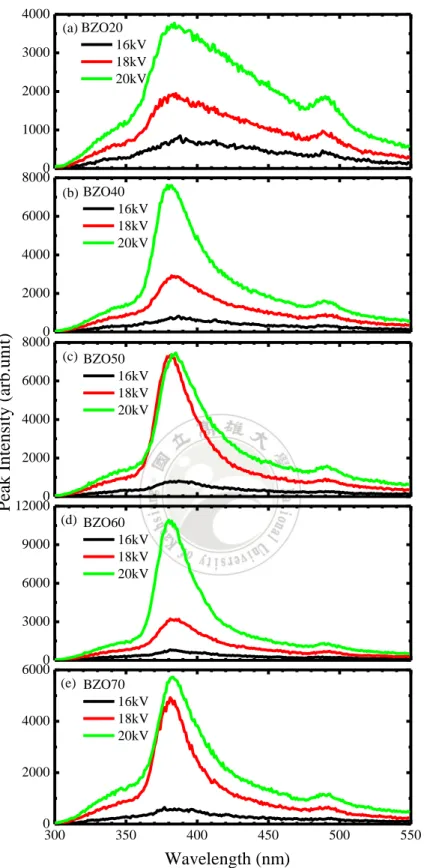
Fig. 1.13 shows CL spectra of samples (a) BZO20, (b) BZO40, (c) BZO50, (d) BZO60, and (e) BZO70 with the excitations of 16, 18, and 20kV electron voltages at room temperature.
In general, thicker films have stronger CL intensities since thicker films have a better crystallization. These results can also be somehow verified by the SEM images which also show that the surface granular textures of the BZO70 sample are larger than those of the BZO20 sample.
In addition, the average ZnO:B grain sizes can be indirectly verified from the results of the CL measurements. Since larger grain size will have more crystalline structures and thus less defects, and therefore stronger CL peak intensity, it can be expected that CL emission intensities are linearly proportional to their associated average grain size. The average ZnO:B grain sizes estimated from the XRD almost fully agree with those from the CL measurements, except for the BZO70 sample in which the CL intensity is smaller than the BZO40, BZO50, and BZO60 samples. This may be due to the spot of the CL measurement on the BZO70 sample has many inferior material defects.
1.4.3 Estimation of strain by Raman scattering measurement
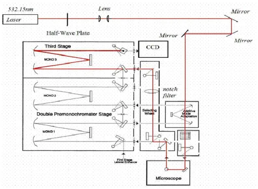
As shown in Fig. 1.14, Raman spectra were recorded in the backscattering configuration using a Jobin Yvon-Horiba Micro-Raman system (model T64000) under a 532 nm excitation laser. A polarizer was set between the laser and the measured sample to polarize the laser light. Raman scattering can measure the frequency shift of phonons and strain distribution of the samples BZO20, BZO40, BZO50, BZO60, and BZO70.
The Raman scattering spectra, as shown in Fig. 1.15, is a useful tool to analyze the strain for crystalline materials by the equation as [11]
) 2 ( ] ) ( ) ( [ 13 33 13 33 2 C C C C a b high E yy xx
where the deformation potential constants a=-580cm-1 and b=-765cm-1 are E2-high mode [12].
Raman frequency shift
EZnO2(High) of E2(High) mode, strain
, Rq, CL, and surfacemorphology of samples BZO20, BZO40, BZO50, BZO60, and BZO70 are shown in Table 1.2. The strains on BZO70 are slightly smaller than those on BZO20, The strains calculated from the Raman scattering strongly agree with those calculated from the XRD.
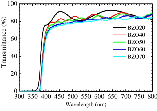
Fig. 2.16 shows the transmittance spectra for the five samples. The ZnO transmittance slightly decreases as the thickness increases. Since samples with larger grain size have more crystalline structures, it can be expected that a thicker sample shows a lower transmittance. The bandgap energy of semiconductor, Eg, can be estimated by extrapolating the linear portion of
the transmittance to zero. As shown in Table 1.2, as the thickness increases, the red-shifted Eg
is consistent with the weaker quantum size effect [14].
1.5 Sample structures and growth conditions of the high-doping ZnO:B films grown on glass substrates
Fig. 1.17 shows the sample structures of the high-doping ZnO:B films grown on glass substrates by LPCVD with different film thicknesses. Glass substrates are prepared and cut
into 2
cm 2
2 pieces. These glass substrates were dipped into 5% HF solutions to remove their native oxide layers and then rinsed in de-ionized water for 3 minutes. The ZnO films with the thickness of 0.391, 0.991, 1.397 and 1.664 μm were deposited on glass substrates, (denoted as the sample BZO20, BZO40, BZO60, and BZO70, respectively) at 170oC temperature by LPCVD. The total pressure for deposition is 0.6 torr. The deposition time for the BZO(0.391μm) to BZO(1.664μm) samples are 20 to 70 min, respectively. Diethylzinc (DEZ) and water (H2O)
vapors carried by argon gas were used as precursors, and their flows were set to 500 and 550 sccm, respectively. The boron doping is accomplished by controlling the flow rate of B2H6 to
1.6 Characterizations and analyses of high-doping ZnO:B grown on glass substrates 1.6.1 X-Ray diffraction and lattice strain
The samples are also analyzed by using the XRD. The results are shown in Fig. 1.18(a). There are three main diffraction peaks from the crystalline ZnO:B grains: (100), (002), and (110) peaks, while the rest of the diffraction peaks are barely noticeable and thus will be ignored in the following discussion. Generally, the percentages of grains associated with different peaks are proportional to their correspondent XRD integrated intensities. As a result, the percentages of (100), (002), and (110) ZnO:B grains obtained from XRD data are shown in Fig. 1.18(b). The peak and integrated intensities, and the full width at half maximum (FWHM) of the (100), (002), and (110) peaks associated with three different crystalline orientations of ZnO:B grains are listed in the Table 1.3. Lattice constants a and c obtained from the XRD peaks of the BZO20, BZO40, BZO60, and BZO70samples are shown in Table 1.4.
Fig. 1.19 shows the peak intensities, FWHMs, and grain percentages of the (100), (002), and (110) XRD peaks of the BZO20, BZO40, BZO60, and BZO70 samples. In addition, Fig.
1.20 shows the grain sizes, strains, and averaged grain sizes obtained from (100), (002), and (110) XRD peaks of these five samples. The ZnO:B grain sizes and the percentages of different ZnO:B grains are obtained from the XRD results.
The ZnO:B grains on glass substrates have three major crystalline orientations: (100), (002), and (110). Their grain size, D, can be calculated from the following formula [10]
cos hkl D
where
hkl,
,
, and
are the FWHM, shape factor (usually 0.9), wavelength, anddiffraction angle of X-rays, respectively. As a result, the average grain sizes associated with different peaks can be calculated by using this formula. The calculated results are shown Table 1.3 that the average grain size of the BZO70 sample are slightly larger than that of the BZO20
sample. These results can also be somehow verified by the SEM images which also show that show that the surface granular textures of the BZO70 sample are larger than those of the BZO20 sample.
The XRD data can be analyzed to obtain not only the percentages of different grain crystal orientations but also the strains associated with them. The strains associated with the diffraction peaks can be calculated by the [10]
t a n 4 h k l
where
hkl
FWHM
, and
is x-ray diffraction. The strains on BZO70 are smaller thanthose on BZO20. From the results of the XRD, the average grain sizes of the high-doping ZnO:B films decrease due to the increases of their average strains.
1.6.2 Scanning electron microscope (SEM), cathodo-luminescence (CL), and atomic force microscopy (AFM) studies
The surface structures from the results of the SEM are shown in Fig. 1.21. As schematically illustrated in Fig. 1.11, the ZnO(100) grains will form a polygon structure with the c-axis parallel to the substrate surface. On the other hand, the ZnO(002) grains will form hexagonal cylinder with or without the pyramidal tip. In addition, the ZnO(110) grains will reveal ridge-like structures to the surface. The SEM images in Fig. 1.21 show that ZnO grains on glass substrates have many ridge-like as well as pyramid-like structures. As a result, it is very difficult to estimate the percentage of these two different structures purely from the SEM images.
Fig. 1.22 shows the AFM images of the 5 μm × 5 μm samples of (a) BZO20 (Rq 9.109nm), (b) BZO40 (Rq 13.96nm), (c) BZO60 (Rq 22.556nm), and (d) BZO70 (Rq 28.44nm). The surface roughness of each sample, Rq, is indicated in the parentheses. However, from the AFM images, the surface roughness of the BZO70 is much sharper than that BZO20. Therefore, from
the results of the AFM images, it can be conjectured that the BZO70 have more ridge-like structures than the hexagonal cylinder ones. These results certainly indicate that The ZnO(110) grains have the largest percentage on the BZO70 sample and thus show their ridge-like structures to the surface. From the SEM and AFM results, it can be concluded the thickest film of the BZO70 sample in this study has the largest percentage the ZnO(110) grains with ridge-like surface structures.
Fig. 1.23 shows CL spectra of the samples (a) BZO20, (b) BZO40, (c) BZO60, and (d) BZO70 with the excitations of 16, 18, and 20kV electron voltages at room temperature. In general, thicker films have stronger CL intensities since thicker films have a better crystallization.
In addition, the average ZnO:B grain sizes can be indirectly verified from the results of the CL measurements. Since larger grain size will have more crystalline structures and thus less defects, and therefore stronger CL peak intensity, it can be expected that CL emission intensities are linearly proportional to their associated average grain size. The average ZnO:B grain sizes estimated from the XRD almost fully agree with those from the CL measurements, except for the BZO70 sample in which the CL intensity is smaller than the BZO60 samples. This may be due to the spot of the CL measurement on the BZO70 sample has many inferior material defects.
1.6.3 Estimation of strain by Raman scattering measurement
The Raman scattering spectra, as shown in Fig. 1.24, is a useful tool to analyze the strain for crystalline materials by the equation as [11]
) 2 ( ] ) ( ) ( [ 13 33 13 33 2 C C C C a b high E yy xx
where the deformation potential constants a=-580cm-1 and b=-765cm-1 are E
Raman frequency shift
EZnO2(High) of E2(High) mode, strain
, Rq, CL, and surfacemorphology of samples BZO20, BZO40, BZO60, and BZO70 are shown in Table 1.4. The strains on BZO70 are smaller than those on BZO20, The strains calculated from the Raman scattering strongly agree with those calculated from the XRD.
Fig. 2.25 shows the transmittance spectra for the four samples. The ZnO transmittance slightly decreases as the thickness increases. Since samples with larger grain size have more crystalline structures, it can be expected that a thicker sample shows a lower transmittance. The bandgap energy of semiconductor, Eg, can be estimated by extrapolating the linear portion of
the transmittance to zero. As shown in Table 1.4, as the thickness increases, the red-shifted Eg
is consistent with the weaker quantum size effect [14].
1.7 Discussion and summary
Low-doping ZnO:B films grown on glass substrates with 0.306, 0.95, 1.077, 1.316 and 1.653 m film thicknesses by a LPCVD are analyzed by XRD, SEM, AFM, CL, and transmittance measurements. For the thinnest low-doping ZnO:B sample, the grain percentage of ZnO(002) is larger than those of the ZnO(110) and ZnO(100). As the thickness increases, the grain percentage of ZnO(110) is the largest and increases gradually. The thinnest low-doping sample almost produces ZnO(002) hexagonal cylinders with or without the pyramidal-tip structures, while the medium and thicker low-doping samples particularly favor the growth of ZnO(110) ridge-like grain structures. These XRD results are shown to strongly agree with the SEM, AFM, CL, and transmittance measurements as well.
High-doping ZnO:B films grown on glass substrates with 0.391, 0.991, 1.397 and 1.664
m film thicknesses by a LPCVD are analyzed by XRD, SEM, AFM, CL, and transmittance measurements. The XRD result shows that the high-doping ZnO:B films particularly favor the growth of ZnO(110) ridge-like grain structures. These XRD results are shown to strongly agree
with the SEM, AFM, CL, and transmittance measurements as well.
The thinnest low-doping sample almost produces ZnO(002) hexagonal cylinders with or without the pyramidal-tip structures, while the thinnest high-doping sample favors the growth of ZnO(110) ridge-like grain structures. Because ZnO(002) hexagonal cylinders with or without the pyramidal-tip structures are sharper than ZnO(110) ridge-like grain structures, the surface roughness of the low-doping ZnO:B sample are significantly larger than that of the high-doping one. This is consistent with the results of the SEM and AFM measurements. For both the low- and high-doping ZnO:B samples, the thicker samples show a larger grain size, a smaller strain, and a lower transmittance. The results of this work provide information for the growth of well-faceted ZnO films by a LPCVD on glass substrates.
References
1. Steinhauser, Jerome. Low pressure chemical vapor deposited Zinc Oxide for thin film silicon solar cells. (Diss. University de Neuchâtel, 2008).
2. D. Panda, and T. Y. Tseng, Journal of Materials Science, 48(20), 6849-6877 (2013). 3. T. Hanada, Oxide and Nitride Semiconductors (pp. 1-19). (Springer Berlin Heidelberg,
2009).
4. C. G. Granqvist, A. Hultaker, Thin Solid Films. 411, 1-5 (2002). 5. J. H. W. De Wit, J. Solid State Chem. 8, 142-149 (1973).
6. P. P. Edwards, A. Porch, M. O. Jones, D. V. Morgan, R. M. Perks, Dalton Trans. 2995-3002 (2004).
7. J. L. G. Fierro, Metal Oxides: Chemistry & Applications. CRC Press. p. 182 (2006). 8. Ü . Ö zgür, Ya. I. Alivov, C. Liu, A. Teke, M. A. Reshchikov, S. Doğan, V. Avrutin,Journal
of Applied Physics 98, 041301 (2005).
9. X.L. Chen, Q. Lin, J. Ni, D.-K. Zhang, J. Sun, Y. Zhao, X.-H. Geng Thin Solid Films 520 1263-1267 (2011)
10. V. D. Mote, Y. Purushotham, B. N. Dole, J. Theor. Appl. Phys. 6 6 (2012).
11. T. Gruber, G. M. Prinz, C. Kirchner, R. Kling, F. Reuss, W. Limmer, and A. Waag, J. Journal of Applied Physics 96, 289 (2004).
12. G. Callsen, J. S. Reparaz, M. R. Wagner, R. Kirste, C. Nenstiel, A. Hoffmann, and M. R. Phillips, Appl. Phys. Lett. 98, 061906 (2011).
13. H. Morkoc and Ü . Ö zgür, Zinc Oxide: Fundamentals, Materials and Device Technology (Weinheim: Wiley-Vch, 2007).
BZO20 BZO40 BZO50 BZO60 BZO70 Peak intensity ZnO(100)
(arb. unit)
104 184 163 182 149
Peak intensity ZnO(002) (arb. unit)
229 63 53 146 216
Peak intensity ZnO(110) (arb. unit)
70 407 643 765 1252
FWHM ZnO(100) (degree) 0.3453 0.33407 0.33363 0.30167 0.25904 FWHM ZnO(002) (degree) 0.43981 0.37348 0.367 0.35402 0.32967 FWHM ZnO(110) (degree) 0.51483 0.42999 0.40607 0.38245 0.35136 Integrated intensity ZnO(100)
(arb. unit)
99.02 128.78 131.54 117.2 109.12 Integrated intensity ZnO(002)
(arb. unit)
150.18 51.5 39.04 103.68 149.42 Integrated intensity ZnO(110)
(arb. unit)
58.42 255.24 358.72 420.46 621.38
Grain percentage ZnO(100) (%)
18.783 21.298 14.685 11.672 5.56 Grain percentage ZnO(002)
(%)
56.309 5.133 1.859 10.831 11.621 Grain percentage ZnO(110)
(%)
24.908 73.569 83.456 77.497 82.819
Grain size ZnO(100) (nm) 43.01436 43.1738 43.23261 47.81237 55.68156 Grain size ZnO(002) (nm) 33.00225 38.862 39.55224 40.99847 44.03026 Grain size ZnO(110) (nm) 30.60414 36.65519 38.81543 41.21418 44.86276 Average grain size (nm) 34.28551 38.15681 39.4778 41.96096 45.36755 Strain ZnO(100) 0.294491 0.293313 0.292758 0.264747 0.227294 Strain ZnO(002) 0.357029 0.303314 0.297698 0.287487 0.267463 Strain ZnO(110) 0.238964 0.199279 0.188171 0.177197 0.162764 Average strain 0.315875 0.224647 0.205566 0.199361 0.178519 Table 1.1 Peak intensities, FWHMs, and integrated intensities of XRD peaks and the corresponding grain percentages, average grain size, and average strain of the low-doping BZO20, BZO40, BZO50, BZO60, and BZO70 samples.
Sample BZO20 BZO40 BZO50 BZO60 BZO70 Thickness (μm) 346.9 950.5 1077.2 1316.8 1653.4
Main grain (002) (110) (110) (110) (110) Surface morphology Hexagonal Ridge Ridge Ridge Ridge Rq (nm) 14.967 34.555 42.875 55.862 60.245
D (nm) of ZnO: B(100) (nm) 43.01 43.17 43.23 47.81 55.68 D (nm) of ZnO: B(110) (nm) 30.60 36.65 38.81 41.21 44.86 D (nm) of ZnO: B(002) (nm) 33.00 38.86 39.55 40.99 44.03 Average grain size (nm) 34.285 38.156 39.477 41.960 45.367
Average strain 0.3158 0.2246 0.2055 0.1993 0.1785
Lattice constant a from ZnO: B(100) (Å ) 3.2509 3.2505 3.2493 3.2491 3.2486 Lattice constant a from ZnO: B(110) (Å ) 3.2513 3.2474 3.2472 3.2468 3.2463 Average a (Å ) 3.2512 3.2499 3.2491 3.2480 3.2470
Lattice constant c from ZnO: B(002) (Å ) 5.2384 --- --- 5.2417 5.2360 CL intensity Weaker Medium Stronger
Eg (eV) 3.329 3.279 3.266 3.257 3.255
Raman shift EZnO(High) 2
(nm-1) --- -0.397 -0.228 -0.206 -0.178
Strain
(%) --- 0.0937 0.0538 0.0486 0.042 Table 1.2 Thickness, main grain, surface morphology, Rq of AFM, grain size (D), lattice constants a and c, CL intensity, and energy gap (Eg) of the low-doping BZO20, BZO40, BZO50,BZO20 BZO40 BZO60 BZO70 Peak intensity ZnO(100) (arb. unit) 168 294 252 170
Peak intensity ZnO(002) (arb. unit) 70 64 80 264
Peak intensity ZnO(110) (arb. unit) 150 642 1096 1328 FWHM ZnO(100) (degree) 0.29023 0.27334 0.27688 0.21548 FWHM ZnO(002) (degree) 0.46245 0.3639 0.35497 0.23581 FWHM ZnO(110) (degree) 0.52395 0.47248 0.41184 0.40832 Integrated intensity ZnO(100) (arb. unit) 77.24 135.2 121.26 85.36 Integrated intensity ZnO(002) (arb. unit) 58.64 78.26 40.24 134.18 Integrated intensity ZnO(110) (arb. unit) 129.12 432.2 692.9 825.84 Grain percentage ZnO(100) (%) 0.274397 0.169678 0.106704 0.066465 Grain percentage ZnO(002) (%) 0.150385 0.032535 0.022193 0.101099 Grain percentage ZnO(110) (%) 0.575217 0.797787 0.871103 0.832436 Grain size ZnO(100) (nm) 49.69914 52.77868 52.09968 66.94478 Grain size ZnO(002) (nm) 31.38875 39.89625 40.90068 61.56231 Grain size ZnO(110) (nm) 30.08517 33.38831 38.30083 38.63467 Average grain size (nm) 35.66323 36.89016 39.83092 42.83425
Strain ZnO(100) 0.254561 0.23923 0.242588 0.18881
Strain ZnO(002) 0.375108 0.294582 0.287292 0.191078 Strain ZnO(110) 0.242705 0.218116 0.190202 0.188497
Average strain 0.265869 0.224186 0.197946 0.188779
Table 1.3 Peak intensities, FWHMs, and integrated intensities of XRD peaks and corresponding grain percentages, average grain size, and average strain of the high-doping BZO20, BZO40, BZO60, and BZO70 samples.
Sample BZO20 BZO40 BZO60 BZO70
Thickness (nm) 391.9 991.3 1397.1 1664.1 Main grain (110) (110) (110) (110)
Surface morphology Ridge-like Ridge-like Ridge-like Ridge-like Rq (nm) 9.109 13.960 22.556 28.440
D (nm) of ZnO: B(100) (nm) 49.69 52.77 52.09 66.94
D (nm) of ZnO: B(110) (nm) 30.08 33.38 38.30 38.63
D (nm) of ZnO: B(002) (nm) 31.38 39.89 40.90 61.56
Average grain size (nm) 35.663 36.890 39.830 42.834 Average strain 0.2658 0.2241 0.1979 0.1887 Lattice constant a from ZnO: B(100) (Å ) 3.2474 3.2409 3.2441 3.2444 Lattice constant a from ZnO: B(110) (Å ) 3.2462 3.2377 3.2387 3.2377 Average a (Å ) 3.2470 3.2404 3.2432 3.2403 Lattice constant c from ZnO:B(002) (Å ) --- --- --- 5.2297 CL intensity Weaker Medium Stronger Eg (eV) 3.382 3.353 3.337 3.334
Raman shift EZnO(High) 2
(nm-1) -2.111 -1.533 -0.677 -0.108
Strain
(%) -0.4986 -0.3621 0.1599 0.0255 Table 1.4 Thickness, main grain, surface morphology, Rq of AFM, grain size (D), lattice constants a and c, CL intensity, and energy gap (Eg) of the high-doping BZO20, BZO40,Figure 1.1 The mineral wurtzite is a crystal structure for various binary compounds
Figure 1.2 SEM images of PET/ZnO thin films at different deposition temperatures: (a) 383 K, Rs ~ 10 k Ω at d ~ 560 nm, (b) 398 K, Rs ~ 2 k Ω at d ~ 720 nm, (c) 423 K, Rs ~ 250 Ω at d ~ 1080 nm, and (d) 428 K, Rs ~ 300 Ω at d ~ 1250 nm.
Figure 1.3 Experimental flow chart of this chapter.
Figure 1.4 Structures of the low-doping BZO20, BZO40, BZO50, BZO60, and BZO70 samples grown on glass substrates. 20, 40, 50, 60, and 70 mean growth times in minutes with corresponding to thicknesses 346.9, 950.5, 1077.2, 1316.8, and 1653.4 nm, respectively.
To investigate transmittance of samples
BZO(20, 40, 50, 60, and 70mins) grown on glass substrates by a LPCVD
Sample preparation
To measure the surface morphology of samples
To investigate strain and grain size of samples
To calculate strain of samples Atomic Force Microscopy (AFM)
Measurement
Raman Measurement X-ray Diffraction (XRD)
Measurement
UV-Visible Transmittance Spectra Study
To investigate microstructures and nanophotonics of samples Scanning Electron Microscope
(SEM) and Cathodoluminescence (CL) Measurements
BZO20 BZO40 BZO50 BZO60 BZO70
0
20
40
60
80
100
30
35
40
45
50
55
60
0
500
1000
1500
2000
2500
3000
Grain Percenta
ge (%)
ZnO (100)
ZnO (002)
ZnO (110)
(b)
ZnO(100) ZnO(002) ZnO(110)Intensity (arb. unit)
2
(degree)
BZO20
BZO40
BZO50
BZO60
BZO70
(a)
Figure 1.5 (a)XRD and (b)grain percentage obtained from XRD peaks of the low-doping BZO20, BZO40, BZO50, BZO60, and BZO70 samples.
0
300
600
900
1200
1500
0.2
0.3
0.4
0.5
0.6
BZO20
BZO40
BZO50
BZO60
BZO70
0
20
40
60
80
100
(c)
(a)
Peak Int
ensi
ty (ar
b.uni
t)
ZnO (100) ZnO (002) ZnO (110)(b)
FWH
M (
degre
e)
ZnO (100) ZnO (002) ZnO (110)G
ra
in Perce
nt
age (
%)
ZnO (100) ZnO (002) ZnO (110)Figure 1.6 (a) Peak intensities, (b) FWHMs, and (c) grain percentages of diffraction peaks ZnO(100), ZnO(002), and ZnO(110) for the low-doping BZO20, BZO40, BZO50, BZO60, and BZO70 samples.
30
35
40
45
50
55
60
0.15
0.20
0.25
0.30
0.35
0.40
G
ra
in si
ze (
nm
)
ZnO(100) ZnO(002) ZnO(110)St
ra
in
ZnO(100) ZnO(002) ZnO(110)BZO20 BZO40 BZO50 BZO60 BZO70
30
35
40
45
50
(c)
(b)
(a)
Averaged grain size XRD strain
Av
er
ag
ed
gr
ain
s
ize (n
m
)
0.15
0.20
0.25
0.30
0.35
X
RD s
tra
in (ar
b. uni
t)
Figure 1.7 (a) Grain size, (b) strain obtained from XRD peaks, and (c) averaged grain size versus XRD strain of the low-doping BZO20, BZO40, BZO50, BZO60, and BZO70 samples.
(a) (b)
Figure 1.8 (a) SEM and (b) CL experimental setups in a JEOL SEM system (model JSM 7000F).
Figure 1.10 SEM images of the low-doping (a) BZO20, (b) BZO40, (c) BZO50, (d) BZO60, and (e) BZO70 samples.
Figure 1.11 ZnO grown on glass substrates. (a) For ZnO(100), a polygon structure for the c-axis growth parallel to the substrate; (b) For ZnO(110), the ZnO grains will reveal ridge-like structures; (c) For ZnO(002), the ZnO grains will form hexagonal cylinder with or without the pyramidal tip; (d) For ZnO(101), the ZnO grains mainly form the pyramidal tip without the hexagonal cylinder.
Figure 1.12 AFM images (5 μm × 5 μm) of the low-doping (a) BZO20 (Rq 14.967nm), (b) BZO40 (Rq 34.555nm), (c) BZO50 (Rq 42.875nm), (d) BZO60 (Rq 55.862nm), and (e) BZO70 (Rq 60.245nm) samples. Surface roughness of each sample, Rq, is shown in the parentheses.
0 1000 2000 3000 4000 0 2000 4000 6000 8000 0 2000 4000 6000 8000 0 3000 6000 9000 12000 300 350 400 450 500 550 0 2000 4000 6000 (a) (e) (d) (c) BZO20 16kV 18kV 20kV Wavelength (nm) (b)BZO40 16kV 18kV 20kV Peak In te n sit y (arb .u n it ) BZO50 16kV 18kV 20kV BZO60 16kV 18kV 20kV BZO70 16kV 18kV 20kV
Figure 1.13 CL spectra of the low-doping (a) BZO20, (b) BZO40, (c) BZO50, (d) BZO60, and (e) BZO70 samples with the excitations of 16, 18, and 20kV electron voltages at room temperature.
Figure 1.14 Experimental setup of Jobin Yvon-Horiba Micro-Raman system (model T64000).
300
350
400
450
500
10000
15000
20000
25000
30000
E2 highInt
ensi
ty (a
rb. uni
t)
Wavelength (nm)
BZO20 BZO40 BZO50 BZO60 BZO70Figure 1.15 Raman spectra of the low-doping BZO20, BZO40, BZO50, BZO60, and BZO70 samples.
300 350 400 450 500 550 600 650 700 750 800
0
20
40
60
80
100
Wavelength (nm) BZO20 BZO40 BZO50 BZO60 BZO70Trans
m
it
tance (
%)
Figure 1.16 Transmittance spectra of the low-doping BZO20, BZO40, BZO50, BZO60, and BZO70 samples.
Figure 1.17 Structures of the high-doping BZO20, BZO40, BZO60, and BZO70 samples grown on glass substrates. 20, 40, 60, and 70 mean growth times in minutes with corresponding to thickness 391.9, 991.3, 1397.1, and 1664.1 nm, respectively.
BZO20
BZO40
BZO60
BZO70
0
20
40
60
80
100
30
35
40
45
50
55
60
0
500
1000
1500
2000
2500
Grain Percenta
ge (%)
ZnO (100)
ZnO (002)
ZnO (110)
(b)
ZnO(100) ZnO(002) ZnO(110)Intensity (arb. unit)
2
(degree)
BZO20
BZO40
BZO60
BZO70
(a)
Figure 1.18 (a)XRD and (b)grain percentage obtained from XRD peaks of the high-doping BZO20, BZO40, BZO60, and BZO70 samples.
0
500
1000
1500
0.2
0.3
0.4
0.5
0.6
BZO20
BZO40
BZO60
BZO70
0
20
40
60
80
100
Peak Int
ensi
ty (ar
b. uni
t)
ZnO (100) ZnO (002) ZnO (110)(c)
(b)
FWH
M (
degre
e)
ZnO (100) ZnO (002) ZnO (110)(a)
G
ra
in Perce
nt
age (
%)
ZnO (100) ZnO (002) ZnO (110)Figure 1.19 (a) Peak intensities, (b) FWHMs, and (c) grain percentages of diffraction peaks ZnO(100), ZnO(002), and ZnO(110) for the high-doping BZO20, BZO40, BZO60, and BZO70 samples.
30
40
50
60
70
0.15
0.20
0.25
0.30
0.35
0.40
G
ra
in si
ze (
nm
)
ZnO(100) ZnO(002) ZnO(110)(c)
(b)
(a)
St
ra
in
ZnO(100) ZnO(002) ZnO(110)BZO20 BZO40 BZO60 BZO70
35
40
45
Averaged grain size XRD strain
Ave
raged grain s
ize
(nm)
0.15
0.20
0.25
0.30
X
RD s
tra
in (ar
b. uni
t)
Figure 1.20 (a) Grain size, (b) strain obtained from XRD peaks, and (c) averaged grain size versus XRD strain of the high-doping BZO20, BZO40, BZO60, and BZO70 samples.
Figure 1.21 SEM images of the high-doping (a) BZO20, (b) BZO40, (c) BZO60, and (d) BZO70 samples.
Figure 1.22 AFM images (5 μm × 5 μm) of the high-doping (a) BZO20 (Rq 9.109nm), (b) BZO40 (Rq 13.960nm), (c) BZO60 (Rq 22.556nm), and (d) BZO70 (Rq 28.440nm) samples. Surface roughness of each sample, Rq, is shown in the parentheses.
0 1000 2000 3000 4000 5000 0 1000 2000 3000 4000 5000 0 1000 2000 3000 4000 5000 300 350 400 450 500 550 0 1000 2000 3000 4000 5000
(a)
BZO20 16kV 18kV 20kV(b)
Wavelength (nm) Peak In te n sit y (arb .u n it ) BZO40 16kV 18kV 20kV(c)
BZO60 16kV 18kV 20kV(d)
BZO70 16kV 18kV 20kVFigure 1.23 CL spectra of the high-doping (a) BZO20, (b) BZO40, (c) BZO60, and (d) BZO70 samples with the excitations of 16, 18, and 20kV electron voltages at room temperature.
300
350
400
450
500
10000
15000
20000
E2 highInt
ensi
ty (a
rb. uni
t)
Wavelength (nm)
BZO20 BZO40 BZO60 BZO70Figure 1.24 Raman spectra of the high-doping BZO20, BZO40, BZO60, and BZO70 samples.
300 350 400 450 500 550 600 650 700 750 800
0
20
40
60
80
100
Wavelength (nm) BZO20 BZO40 BZO60 BZO70Trans
m
it
tance (
%)
Figure 1.25 Transmittance spectra of the high-doping BZO20, BZO40, BZO60, and BZO70 samples.
Chapter 2 Characterizations and analyses of the pressure- and
doping-dependent ZnO:B films grown on glass substrates by a low-pressure
chemical vapor deposition
2.1 Introduction
Boron-doped zinc oxide (BZO) grown by a low pressure chemical vapor deposition (LPCVD) at 175°C shows some unique features for the use as transparent conductive oxide in thin film silicon solar cells [1]. The native surface texture that can be tailored by the deposition conditions results in excellent light scattering properties, in combination with high transparency and low surface resistance. The major disadvantage of this material is the sensitivity to humidity. For a long term operation, a good encapsulation is required, otherwise a degradation causing increased sheet resistance.
BZO samples have been studied with a variation of diborane flow rate [2]. In Fig. 1(a), the feature size from SEM images at a high doping gas flow decreases, while the haze decreases. In Fig. 1(b), the sheet resistance is saturated at 3 sccm gas flow, while the film thickness is mainly unaffected. The hall measurements show the carrier concentration saturates, while the mobility of carriers decreases at higher levels of doping gas flow. This decrease in mobility may be explained by scattering at ionized impurities in the film.
2.2 Motivation and investigation procedures
In this chapter, the pressure- and doping-dependent ZnO:B thin flims grown on glass substrates by a LPCVD were investigated.
Fig. 2.2 shows the experimental procedures of this study. The growth methods and conditions of ZnO:B thin films on glass substrates will be described in the section 2.3. The surface morphologies of samples are measured by the atomic force microscopy (AFM) and scanning electron microscope (SEM) measurements. The film quality and optical properties of
the samples are studied by the cathodoluminescence (CL). The crystallization of ZnO grains and their properties are determined by X-ray diffraction (XRD) measurement. The strains of ZnO:B grains are analyzed by Raman scattering measurement. Analyzing the results of these measurements, we will discuss the characteristics and properties of the pressure- and doping-dependent ZnO:B thin flims grown on glass substrates. The experimental results and their theoretical explanations will be discussed in the Section 2.4. A brief conclusion will be summarized in the Section 2.7.
2.3 Sample structures and growth conditions of the pressure-dependent ZnO:B films grown on glass substrates
Fig. 2.3 shows the sample structures of the pressure-dependent ZnO:B grown on glass substrates by a low pressure chemical vapor deposition (LPCVD). Glass substrates are prepared and cut into 2
cm 2
2 pieces. Two ZnO:B films with 0.4 and 0.6 torr growth pressures and 1.209 and 1.013 μm in thickness (denoted as the samples BZO0.4, and BZO0.6, respectively)
were deposited on glass substrates at 170oC temperature by a LPCVD. The deposition time is
70 mins. Diethylzinc (DEZ) and water (H2O) vapors carried by argon gas were used as
precursors, and their flows were set to 500 and 550 sccm, respectively. The boron doping is accomplished by controlling the flow rate of B2H6 to be 5 sccm.
2.4 Characterizations and analyses of the pressure-dependent ZnO:B films grown on glass substrates
2.4.1 X-Ray diffraction and lattice strain
The sample structures are analyzed by using the XRD. The results are shown in Fig. 2.4(a) There are three main diffraction peaks from the crystalline ZnO:B grains: (100), (002), and (110) peaks. Generally, the percentages of grains associated with different peaks are proportional to their correspondent XRD integrated intensities. As a result, the percentages of
(100), (002), and (110) grains obtained from XRD data are shown in Fig. 2.4(b). The peak integrated intensities, full width at half maximum (FWHM), and grain percentages of the (100), (002), and (110) peaks associated with three different crystalline orientations of ZnO:B grains are listed in the Table 2.1. Lattice constants a and c obtained from the XRD peaks of the BZO0.4
and BZO0.6 samples are shown in Table 2.2.
Fig. 2.5 shows the peak intensities, FWHMs, and grain percentages of the (100), (002), and (110) XRD peaks of the BZO0.4 and BZO0.6 samples. In addition, Fig. 2.6 shows the grain
sizes, strains, and averaged grain sizes obtained from (100), (002), and (110) XRD peaks of the two samples.
The ZnO:B grains on glass substrates have three major crystalline orientations: (100), (002), and (110). Their grain sizes D can be calculated from the following formula [3]
cos hkl D
where
hkl,
,
, and
are the FWHM, shape factor (usually 0.9), wavelength, anddiffraction angle of X-rays, respectively. As a result, the average grain sizes associated with different peaks can be calculated by using this formula. As shown in Table 2.1, the average grain size of the BZO0.4 sample on the glass substrate are larger than that of the BZO0.6 sample.
These results can also be somehow verified by the SEM images which also show that the surface granular textures on the BZO0.4 sample are slightly larger than those on the BZO0.6
sample.
The XRD data can be analyzed to obtain not only the percentages of different grain crystal orientations but also the strains associated with them. The strains associated with the diffraction peaks can be calculated by the [3]
t a n 4 h k l