A Tree-Block Scheduling Architecture for Separable 2-D Inverse Discrete Wavelet Transform
8
0
0
全文
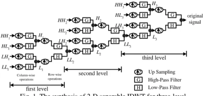
(2) IV, we describe the proposed VLSI architecture. Then in Section V, we show the proposed architecture can be easily scalable for different filter lengths and different octave levels. In Section VI, we present some results. Finally, some conclusions are presented in Section VII.. sis. An N×N sequence of input data can be represented as Fig. 2(a). At the beginning of processing, the finer-coefficient subband labeled LL2 in Fig. 2(b) is first reconstructed from the four coarsest subbands LL1 , LH1, HL1 , and HH1 in Fig. 2(a), and then the four subband LL2, LH2, HL2, and HH2 is used further to obtain the next finer scaled wavelet coefficients. This processing continues until the original image of size N × N is reconstructed (see Fig. 1(a)→(b)→(c)→(d)). Note that, because of the up sampling required for both column-wise and row-wise processing, the size of the synthesized subband is four times larger than the original after one level processing. Then, the required computation in the next level is relatively increased.. 2. INVERSE DISCRETE WAVELET TRANSFORM. HH1. 2. HL1. 2. LH1. 2. G. LL1. 2. H. H1. G. 2. H. G. 2. H. G. 2. G. H. 2. H. 2. HL2. 2. H. LH3 G. LH2 G. 2. G. H. 2. H. H 2. 2. 2. 2. L3. LL3. L2. third level 2 G. second level. Row-wise operations. original signal. 2. LL2. L1. Column-wise operations. H2. 2. HL3. HH2. G. H3. HH3. H. first level. Up Sampling. 3. TREE-BLOCK SCHEDULE. High-Pass Filter Low-Pass Filter. Fig. 1. The synthesis of 2-D separable IDWT for three-level.. We propose a new scheme for the 2-D IDWT called tree-block pipelining schedule. In this scheme, the schedule of the input subband coefficients is based on the depth-first (block-first) traverse, while the previous methods are based on the breadth-first (level-first) traverse [2]-[4]. Specifically, the breadth-first traverse just like Fig.1 first inputs the four coarsest subbands to reconstruct the finer subband that is further used with three other subbands in the next level; the processing is repeated level by level until the original image is reconstructed. In such method, at each level, the processing cannot be started until the four wavelet subbands are obtained, so this breadth-first traverse will need a great amount buffers to store temporal low-low subbands. For example, an N×N input sequence for the computation of three-level IDWT at least requires N 2 / 4 temporary buffers to store the finest subband coefficients; it is impractical for high-resolution image frame. Besides, waiting the produced coefficients makes the hardware idle some time, as a result, such design increases the overall computation time.. The IDWT processes the input signal subbands from the coarsest resolution level to the finest one. Generally, the 2-D IDWT computation can be classified into separable and non-separable types according to its operating manner. Here we only consider the separable type. Fig. 1 shows the computation of a three-level 2-D separable IDWT synthesis process, in which each level is composed of two types of processing, the column-wise processing and the row-wise processing. Each processing consists of the high-pass filtering (G), the low-pass filtering (H), and up sampling. We denote the four inputs at dth-level computation along the column by HHd, HLd, LHd, and LLd, and denote the two inputs at dth-level computation along the row by Hd and L d. Suppose that the length of filter (or filter tap) is of size K, the transfer functions of filters H and G are represented as follows: K −1. K −1. k =0. k =0. H(z)= ∑ hk z − k , G(z)= ∑ g k z − k In the following section we first present our proposed architecture with four filter taps for both H(z) and G(z) and with three-level reconstruction for example, and then we will show it can be easily scalable for different filter lengths and different octave levels. N 8 N N 4 N 2. LL1 HL1 LH1 HH1. HL2. LL2. HL3. LH2 HH2. LH3. first level synthesis. HH3. LL1 HL1. B(0,0) B(0,1). LH1 HH1. HL2. LH2. HH2. HL3. LH3. HH3. ... .... B(1,0). HL2. HL3. LH2 HH2. LH3. (a). HH3. (b). Fig. 3. Reorganizing of a wavelet tree into a wavelet block. (a). LL3. second level synthesis. HL3. LH3. third level synthesis. (b). However, the tree-block scheduling, at the beginning, divides all the input subband coefficients into several wavelet trees [13]. Each tree contains a tree root, which is one coefficient in the coarsest subband, and its descendants, which are the coefficients relative to the tree root in all the finer scale subbands (see Fig. 3(a)). Then, the coefficients of each wavelet tree are reorganized to form a wavelet block as shown in Fig. 3(b) where B(i,j) represents the wavelet block at location (i,j). The concept of the wavelet block provides an association between wavelet coefficients and what they represent spatially in the image frame. Therefore, this scheduling scheme processes the frame. Original image. HH3 (c). (d). Fig. 2. An example for the processing of 2-D 3-level IDWT.. Now, we look close to the procedure of the reconstruction. Let us consider a three level 2-D IDWT for image synthe2.
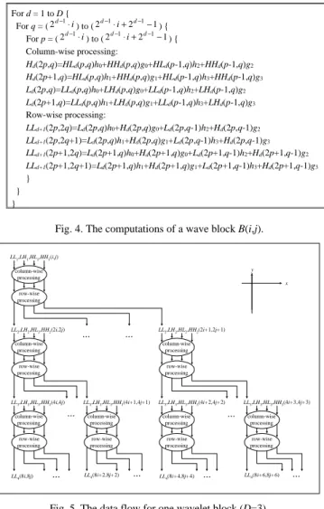
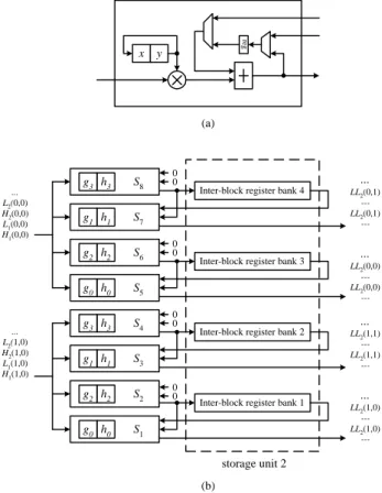
(3) block by block for all levels not level by level until the whole frame is reconstructed. The advantages of the block-based processing are that (1): The next level computations within the same block can be started as early as possible and are easily pipelined to get a higher performance, and (2): the size of a wavelet block is invariant and is less than the image size, so the size of buffer for storing temporal data is greatly reduced from the whole frame size to the size of a wavelet block. For a D-level IDWT, we need only 4 D−1 temporary buffers and the value of D is always small.. x-direction and y-direction onto one processor. Then, an efficient architecture for 2-D IDWT computation is derived. Fig. 6 presents the block diagram of this high performance and low cost VLSI architecture, which is composed of one column filter, one row filter, two storage units, and a temporary buffer unit. From Fig. 4, the proposed inverse architecture first performs the column filtering and then the row filtering to process the decomposed subbands. Note that the two efficient filter structures are used to process the computation of each wavelet block in the row major order for all levels. The column filtering computes along the columns and produces the outputs in the row major order. The row filtering read the data from the column filtering and computes along the rows and produces the outputs in the row major order. The two storage units store the partial results for the column and row filtering, which will be used within current block or in other blocks. The temporary buffer unit stores the subband LLd(for d >1) of a wavelet block. The details of each component are described in the following discussions. We first present our proposed architecture with four filter taps for both H(z) and G(z) and with three-level reconstruction for example, and then we will show it can be easily scalable for different filter lengths and different octave levels.. We assume that the synthesized level is D, and that the size of synthesized image is N×N. Thus, the input sequence is divided into N 2 / 4 D wavelet blocks each of which is of size 2 D × 2 D . Each wavelet block B(i,j) contains 4 coefficients at the first level, which are LL1(i,j), LH1(i,j), HL1(i,j) and HH1(i,j), 12 coefficients at the second level, which are LH2(2i+r,2j+s), HL2(2i+r,2j+s), and HH2(2i+r,2j+s) for 0 ≤ r , s ≤ 1 , 48 coefficients at the third level, which are LH3(4i+r,4j+s), HL3(4i+r,4j+s), and HH3(4i+r,4j+s) for 0 ≤ r, s ≤ 3 , and 3 ⋅ 2d +1 coefficients at the dth level, which are LHd( 2l −1 i+r, 2l −1 j+s), HLd( 2l −1 i+r, 2l −1 j+s), and HHd( 2l −1 i+r, 2l −1 j+s) for 0 ≤ r , s ≤ 2l −1 − 1 . Here LLd(x,y), LHd(x,y), HLd(x,y), and HHd(x,y) represent the wavelet coefficients at the coordinate (x,y) in the subband LLd, LHd, HLd, and HHd, and Ld(x,y) and Hd(x,y) represent the wavelet coefficients at the coordinate (x,y) in subband Ld and HHd, respectively. The scheduling procedure for a wavelet block B(i,j) is described below.. For d = 1 to D { d −1 d −1 d −1 −1 ) { For q = ( 2 ⋅ i ) to ( 2 ⋅ i + 2 d −1 d −1 d −1 −1) { For p = ( 2 ⋅ i ) to ( 2 ⋅ i + 2 Column-wise processing: Hd(2p,q)=HLd(p,q)h0+HHd(p,q)g0+HLd(p-1,q)h2+HHd(p-1,q)g2 Hd(2p+1,q)=HLd(p,q)h1+HHd(p,q)g1+HLd(p-1,q)h3+HHd(p-1,q)g3 Ld(2p,q)=LLd(p,q)h0+LHd(p,q)g0+LLd(p-1,q)h2+LHd(p-1,q)g2 Ld(2p+1,q)=LLd(p,q)h1+LHd(p,q)g1+LLd(p-1,q)h3+LHd(p-1,q)g3 Row-wise processing: LLd+1(2p,2q)=Ld(2p,q)h0+Hd(2p,q)g0+Ld(2p,q-1)h2+Hd(2p,q-1)g2 LLd+1(2p,2q+1)=Ld(2p,q)h1+Hd(2p,q)g1+Ld(2p,q-1)h3+Hd(2p,q-1)g3 LLd+1(2p+1,2q)=Ld(2p+1,q)h0+Hd(2p+1,q)g0+Ld(2p+1,q-1)h2+Hd(2p+1,q-1)g2 LLd+1(2p+1,2q+1)=Ld(2p+1,q)h1+Hd(2p+1,q)g1+Ld(2p+1,q-1)h3+Hd(2p+1,q-1)g3 } } }. At Level d: (1) For 0 ≤ r , s ≤ 2d −1 − 1 , schedule HHd(2d-1i+r, 2d-1j+s) and HLd(2d-1i+r, 2d-1j+s) at time T + (2/3)(4d-1-1) + 2(2d-1r+s). Compute the outputs Hd(2di+2r, 2d −1 j+s) and Hd(2di+2r+1, 2d-1j+s). Schedule LLd(2di+r,2dj+s) and LHd(2di+r,2dj+s) at time T + (2/3)(4d-1-1) + 2(2dr+s) + 1. Compute the outputs Ld(2di+2r, 2d-1 j+s) and Ld(2d i+2r+1, 2d-1 j+s). d −1. Fig. 4. The computations of a wave block B(i,j). LL1,LH1,HL1,HH1(i,j). (2) For 0 ≤ r , s ≤ 2 − 1 , schedule Hd(2 i+2r, 2 j+s) and Hd(2di+2r+1, 2d-1j+s) at time T + (2/3)(4d-1-1) + 2(2d r+s)+1, and schedule Ld(2di+2r, 2d-1j+s) and Ld(2di+2r+1, 2d-1j+s) at time T+(2/3)(4d-1-1)+2(2dr+s)+2. Compute LLd(2di+2r, 2dj+2s), LLd(2di+2r, 2dj+2s+1), LLd(2di+2r+1, 2dj+2s), and LLd(2di+2r+1, 2dj+2s+1). d. d-1. y. column-wise processing. x row-wise processing. LL2,LH2,HL2,HH2(2i,2j). It can be seen that the procedure is executed block by block in the row major order. Thus, the beginning time T in each wavelet block B(i,j) can be calculated as 2 D N (4 − 1) × (i + j × D ) . 3 2. .... LL2,LH2,HL2,HH2(2i+1,2j+1). .... column-wise processing. column-wise processing. row-wise processing. row-wise processing. LL3,LH3,HL3,HH3(4i,4j). row-wise processing. LL4(8i,8j). LL3,LH3,HL3,HH3(4i+1,4j+1). .... column-wise processing. .... LL3,LH3,HL3,HH3(4i+2,4j+2). column-wise processing. column-wise processing. row-wise processing. row-wise processing. LL4(8i+2,8j+2). .... LL4(8i+4,8j+4). LL3,LH3,HL3,HH3(4i+3,4j+3). .... column-wise processing row-wise processing. .... LL4(8i+6,8j+6). .... 4. PROPOSED ARCHITECTURE Fig. 5. The data flow for one wavelet block (D=3).. Based on the tree-block scheduling described in Section III, the computations of a wavelet block B(i,j) is shown in Fig. 4. According to the equations in Fig. 4, the data flow of the tree-block architecture is drawn in Fig. 5. To minimize the hardware cost, the data flow can be folded along. We now list the equations for column filtering in the dth level. Here we only show the equations for computing the outputs Hd(i,j) because the equations for computing Ld(i,j) is similar to the ones for Hd(i,j). The equations are shown 3.
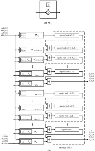
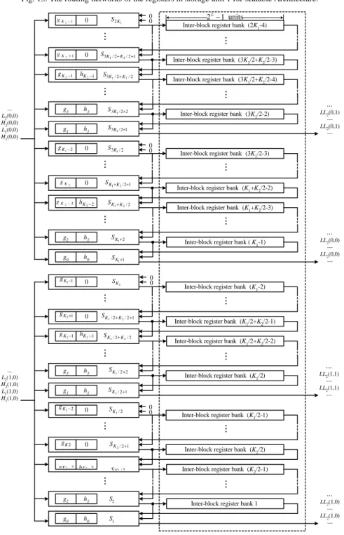
(4) Hd(m,n)=HLd(m,n)h0+HHd(m,n)g0+Pd(m,n). as follows. (1). [Pd(m,n)=HLd(m-1,n)h2+HHd(m-1,n)g2].. Hd(m+1,n)=HLd(m,n)h1+HHd(m,n)g1+HLd(m-1,n)h3+HHd(m-1,n)g3.. (2). Hd(m+1,n)=HLd(m,n)h1+HHd(m,n)g1+Pd(m+1,n) [Pd(m+1,n)=HLd(m-1,n)h3+HHd(m-1,n)g3].. Hd(m+2,n)=HLd(m+1,n)h0+HHd(m+1,n)g0+HLd(m,n)h2+HHd(m,n)g2.. (3). Hd(m+3,n)=HLd(m+1,n)h1+HHd(m+1,n)g1+HLd(m,n)h3+HHd(m,n)g3.. (4). Hd(m,n)=HLd(m,n)h0+HHd(m,n)g0+HLd(m-1,n)h2+HHd(m-1,n)g2.. Pd(m+2,n)=HLd(m,n)h2+HHd(m,n)g2. Pd(m+3,n)=HLd(m,n)h3+HHd(m,n)g3.. Hd(m+4,n)=HLd(m+2,n)h1+HHd(m+2,n)g1+HLd(m+1,n)h3+HHd(m+1,n)g3.. where Pd(m,n), Pd(m+1,n), Pd(m+2,n), and Pd(m+3,n) represent the partial sums of Hd(m,n), Hd(m+1,n), Hd(m+2,n), and Hd(m+3,n), respectively. To store these partial sums of the finer coefficients, storage unit 1 is used for column filtering as shown in Fig. 7(b). It can be seen that there are two register banks in storage unit 1. Based on the concept of wavelet block, each register bank consists of two types of register sub-banks, one for intra-block storing and another for inter-block storing, which are implemented with shift register routing networks shown in Fig. 8. Intra-block sub-bank with the size of 8 units stores the partial sums that will be used within the current wavelet block, while Inter-block sub-banks with the size of 2N units store the partial sums that will be used in the other wavelet block. Here we need an inter-block sub-bank in each level because the lifetimes of inter-block sub-banks in different levels are overlap. Since the column filtering computes the outputs in the row major order, we must store the partial sums of one-row coefficients. Thus, the size of the inter-block sub-bank for dth level is relative to the image size N N and level d and is of size 3− d . An example for the 2 scheduling for the column filtering in a wavelet block is shown in Fig. 9, where Qd represents the partial sum of Ld(m,n). To understand the difference between the inter-block registers and intra-block registers, for instance, P1(2,0) and P1(3,0) in Fig. 9 belong to the other block, and they will be store in inter-block register bank. P2(2,0) and P2(3,0) are stored in intra-block register bank since they are within current wavelet block and will be used in the 7th clock cycle.. .... From the above computations, it can be seen that the coefficient HHd(m,n) appears in all the four equations ( equation (1)-(4)) and so does the coefficient HLd(m,n). If we can process the four equations in parallel, the storage access times of HHd(m,n) and HLd(m,n) will be reduced and the computation time will speed up. According to this idea, the column filter is designed with four modules, Mu, where 1 ≤ u ≤ 4 . Each of them has the same structure and calculates one of the four equations. Fig. 7(a) and Fig. 7(b) show the structure of module Mu and the block diagram of the column filter, respectively. The module Mu consists of two multipliers and one adder. The 2n-to-n reduced width multipliers we developed [15] are used here to reduce the area. When n is large enough, the 2n-to-n multiplier needs only half area of a standard parallel multiplier. To reach higher performance, two registers are inserted into the output for pipelining with the row filter. Storage Unit 1 registers. wavelet cofficients. Storage Unit 2. Column Filter. Row Filter. Temporary Buffer. original image. LLd(d>1). Fig. 6. The block diagram of the tree-block architecture. x. ... LH2(0,0) HH2(0,0) LH1(0,0) HH1(0,0). ... LL2(0,0) HL2(0,0) LL1(0,0) HL1(0,0). y. (a) Mu. N units Inter-block register sub-bank level 3. N/2 units. g3 h3. M4. g1 h1. M3. g2 h2. M2. g0 h0. register bank 2. register bank 1. M1 (b). Inter-block register sub-bank level 2. Pd(m+2,n) or Qd(m+2,n). ... L2(0,0) H2(0,0) L1(0,0) H1(0,0). Pd(m,n) or Qd(m,n). N/4 units Inter-block register sub-bank level 1. 8 units Intra-block register sub-bank. Fig. 8. The routing networks of the registers in storage unit 1.. ... L2(1,0) H2(1,0) L1(1,0) H1(1,0). storage unit 1. Fig. 7. (a) The structure of M(u) and (b) The block diagram of the column filter.. Time unit. Input. 1 2 3 4 5 6 7 8. HH1(0,0), HL1(0,0) LH1(0,0), LL1(0,0) HH2(0,0), HL2(0,0) LH2(0,0), LL2(0,0) HH2(0,1), HL2(0,1) LH2(0,1), LL2(0,1) HH2(1,0), HL2(1,0) .... Input / Read from storage unit 1 P1(0,0), P1(1,0) Q1(0,0), Q1(1,0) P2(0,0), P2(1,0) Q2(0,0), Q2(1,0) P2 (0,1), P2(1,1) Q2(0,1), Q2(1,1) P2(2,0), P2(3,0) .... Output H1(0,0), H1(1,0) L1(0,0), L1(1,0) H2(0,0), H2(1,0) L2(0,0), L2(1,0) H2(0,1), H2(1,1) L2(0,1), L2(1,1) H2(2,0), H2(3,0) .... Output/ Write to storage unit 1 P1(2,0), P1(3,0) Q1(2,0), Q1(3,0) P2(2,0), P2(3,0) Q2(2,0), Q2(3,0) P2(2,1), P2(3,1) Q2(2,1), Q2(3,1) P2(4,0), P2(5,0) .... Fig. 9. The schedule for the column filtering.. In Fig. 7(b), two coefficients, HHd(m,n) and HLd(m,n), are fed simultaneously into four modules to compute the four equations in parallel, but the results are only the partial sums of the product terms of four finer coefficients, Hd(m,n), Hd(m+1,n), Hd(m+2,n), and Hd(m+3,n). Thus, equation (1) to (4) should be changed as follows:. The equations for the row filtering, which are analogous to column filtering, are shown as follows.. 4. LLd+1(m,n)=Ld(m,n)h0+Hd(m,n)g0+Ld(m,n-1)h2+Hd(m,n-1)g2. (5). LLd+1(m,n+1)=Ld(m,n)h1+Hd(m,n)g1+Ld(m,n-1)h3+Hd(m,n-1)g3. (6).
(5) LLd+1(m,n+2)=Ld(m,n+1)h0+Hd(m,n+1)g0+Ld(m,n)h2+Hd(m,n)g2. (7). LLd+1(m,n+3)=Ld(m,n+1)h0+Hd(m,n+1)g0+Ld(m,n)h2+Hd(m,n)g2. (8). size is 4d −1 for dth level. These temporal coefficients in buffer will be soon used in the next level. An example for the scheduling for the row filtering in a wavelet block is shown in Fig. 11.. LLd+1(m,n+4)=Ld(m,n+2)h0+Hd(m,n+2)g0+Ld(m,n+1)h2+Hd(m,n+1)g2 …. Time unit 2 3 4 5 6 7 8 9 10 11 …. From above, Ld(m,n) and Hd(m,n) are in all of the four equations, so the idea of parallel processing is also considered. Besides, without storing the results, our design starts row filtering as soon as the results of the column filtering are produced. According to the scheduling in Fig. 9, two finer coefficients are produced every clock cycle in the column filtering, such as Ld(m,n) and Ld(m+1,n), so that the row filter must compute eight equations in parallel. Based on these concepts, the row filter is designed with eight modules, Su, where 1 ≤ u ≤ 8 . All of them have the same architecture and deal with the partial sum of eight equations.. y. 5. SCALABILITY FOR THE IDWT In this section, we will show the extension for difference filter tap and different levels of the proposed architecture. When the high-pass filter tap extends to K1 and the low-pass filter tap extends to K2 (suppose K1>K2, and K1 and K2 are both even.), the equations for column filtering in the dth level are changed as follows.. (a). ... L2(0,0) H2(0,0) L1(0,0) H1(0,0). ... L2(1,0) H2(1,0) L1(1,0) H1(1,0). g3 h3. S8. g1 h1. S7. g2 h2. S6. g0 h0. S5. g3 h3. S4. g1 h1. S3. g2 h2. S2. g0 h0. 0 0. 0 0. 0 0. 0 0. H d (m + 2k , n ) = ... Inter-block register bank 4. Inter-block register bank 3. LL2(0,1) --LL2(0,1) ---. Inter-block register bank 1. S1. K2 −1 2. ∑ HL ( m + k − p, n )h d. p =0. H d (m + 2k + 1, n ) =. 2p. +. K1 −1 2. ∑ HH q =0. K2 −1 2. ∑ HL ( m + k − p, n)h. 2 p +1. d. p =0. +. (m + k − q, n) g2 q .. d. K1 −1 2. ∑ HH q =0. d. (m + k − q, n) g2 q +1.. for k = 0, 1, 2, …, (K1-1).. ... LL2(0,0) --LL2(0,0) ---. It can be observed that HLd(m,n) appears in the first K2 equations and HHd(m,n) appears in all the K1 equations. Similarly, to reduce the storage access times, the architecture for column filtering, which is changed to Fig. 12(b), needs K2 Mu-modules and (K1-K2) M′u-modules to calculate these K1 equations at the same time. The structure of M′u-module is presented in Fig. 12(a). These K2 Mu-modules compute the partial sum of the first K2 equations every time while (K1-K2) M′u-modules compute the partial sum of the other (K1-K2) equations. To store these partial sums, the storage unit 1 needs (K1-2) register banks and each register banks are the same as Fig. 13. The total size of storage unit 1 is calculated as follows. Total size = (Intra-block registers + Inter-block registers) × number of register banks N N = ( N + + ... + D −1 + 2 D )×(K1-2) ≈ 2(K1-2) ×N 2 2 units The equations for the row filtering with K1 high-pass filter tap and with K2 low-pass filter tap are shown as follows.. ... Inter-block register bank 2. Output LL2(0,0),LL2(0,1),LL2(1,0),LL2(1,1) LL3(0,0),LL3(0,1),LL3(1,0),LL3(1,1) LL3(0,2),LL3(1,3),LL3(1,2),LL3(1,3) LL3(2,0),LL3(2,1),LL3(3,0),LL3(3,1) LL3(2,2),LL3(2,3),LL3(3,2),LL3(3,3) …. Fig. 11. The schedule for the row filtering.. reg. x. Input H1(0,0),H1(1,0) L1(0,0),L1(1,0) H2(0,0),H2(1,0) L2(0,0),L2(1,0) H2(0,1),H2(1,1) L2(0,1),L2(1,1) H2(2,0),H2(3,0) L2(2,0),L2(3,0) H2(2,1),H2(3,1) L2(2,1),L2(3,1). LL2(1,1) --LL2(1,1) ---. ... LL2(1,0) --LL2(1,0) ---. storage unit 2 (b). Fig. 10. (a) The structure of S(u). (b) The block diagram of the row filter.. Fig. 10(a) and Fig. 10(b) show the structure of module Su and the block diagram of the row filter, respectively. In module Su, we also use the 2n-to-n reduced width multipliers to reduce the area. Similar to the column filter, storage unit 2, which is shown in Fig. 10(b), is used here for storing the partial results of coefficients. It only consists of inter-block registers with each size of 7 units because the partial sum of intra-block coefficients will be soon used in the next clock cycle. The partial sum of intra-block coefficients are immediately written to and read from the registers in module Su. Note that the row filtering processes the wavelet blocks in the row major order, so the lifetime of inter-block registers in a block is the time to process a wavelet block. The produced coefficients of subband LLd (for d >1) are stored in the temporary buffer unit whose. LLd +1 ( m, n + 2k ) =. K2 −1 2. ∑L. d. ( m , n + k − p ) h2 p +. p =0. LLd +1 ( m, n + 2k + 1) =. ∑L. d. ( m, n + k − q ) g 2 q .. q =0. K2 −1 2. ∑L. d. p =0. K1 −1 2. ( m, n + k − p )h2 p +1 +. K1 −1 2. ∑L. d. q =0. ( m, n + k − q ) g 2 q +1 .. for k = 0, 1, 2, …, (K1-1).. From above, Ld(m,n) appears in the first K2 equations and 5.
(6) Hd(m,n) appears in all the K1 equations, so the row filtering consists of 2K1 Su-modules as shown in Fig. 14. The K1 Su-modules compute the K1 equations for Ld(m,n), and the other K1 Su-modules compute the K1 equations for Ld(m+1,n). Similarly, those Su-modules calculate only partial sums of the equations, which must be stored in the storage unit 2. The storage unit 2 includes 2(K1-2) in-. that the required buffers stored the temporary subband can be greatly reduced because wavelet coefficients are processed block by block and that the scheduling make the data flow tight and regular to meet high speed and low complexity. Based on this technique, an efficient VLSI architecture have been designed and implemented. To minimize the hardware cost, the architecture utilized two efficient filter structures with reduced width multipliers to accomplish the computation of all octave levels. Moreover, each filter in the architecture is designed regularly and modularly, so it is easily scalable for different filter lengths and different IDWT octave levels by adding some extra modules. Additionally, both column and row filters achieve the 100% resource utilization. Due to its small storage size, regularity, and high performance, the architecture is suited to time-critical applications, such as MPEG-4 and JPEG-2000.. ter-block register banks, each of which is of size 2 D − 1 . The total size of storage unit 2 is calculated as follows. Total size =Inter-block registers × number of register banks =( 2 D − 1 )×(2K1−4) units 6.. RESULTS. It can be seen from the scheduling described in Section III that it requires two cycles to process the four coefficients in the first level and requires eight cycles to process the sixteen coefficients in the second level within a wavelet block. If the octave level extends to D, the number of cycles to process one wavelet block is as follows. Cycles = 2 + 8 + 32 + ... + 2 ⋅ 4. ( D −1). Architectures Multipliers. 2 = (4 D − 1) . 3. Adders. Storage Size. Direct. K. K. N. [8]. 1 3 K 2. K 7( − 1) + 4 2. NK. RAM. N. [11]. 4K. 4K-4. NK/2. RAM. N. Tree-Block. 4K. 4K-2. 2N(K-2). Register. 2 2 N 3. Storage Type RAM. Computing Time Control unit 2. 4N. 2. 2. Simple Complex Simple Simple. Table I. The comparison of various IDWT architectures.. Thus, the total number of cycles for processing an N×N image is shown below:. 8. CONCLUSION. Total Cycles = the number of wavelet blocks × Cycles for one block =. 2. In this paper, we proposed a tree-block scheduling scheme for 2-D separable IDWT. The advantage of this scheme is that the required buffers stored the temporary subband can be greatly reduced because wavelet coefficients are processed block by block and that the scheduling make the data flow tight and regular to meet high speed and low complexity. Based on this technique, an efficient VLSI architecture have been designed and implemented. To minimize the hardware cost, the architecture utilized two efficient filter structures with reduced width multipliers to accomplish the computation of all octave levels. Moreover, each filter in the architecture is designed regularly and modularly, so it is easily scalable for different filter lengths and different IDWT octave levels by adding some extra modules. Additionally, both column and row filters achieve the 100% resource utilization. Due to its small storage size, regularity, and high performance, the architecture is suited to time-critical applications, such as MPEG-4 and JPEG-2000.. 1 2 2 D 2 1 N × (4 − 1) = (1 − D ) N 2 . 4D 3 3 4. When D is large, it needs at most (2 / 3)N 2 cycles to process an image frame. In addition, the schedule also shows that both row filter and column filter achieve 100% hardware utilization and that the data flow is kept regularly. The total size of two storage units for an N×N image is as follows. Total Size = storage unit 1 + storage unit 2 + temporary buffer ≈ 2(K−2)×N+( 2 D − 1 )×(2K−4)+ 4 D−1 Units. When N is large enough, such as 512 or 1024, the total storage size need only 2 N ( K − 2) units. Based on the proposed 2-D IDWT architecture, we compare, in Table I, the characteristics of various architectures with respect to the number of multipliers, the number of adders, storage size, storage type, and computing time. Let the filter tap be K and the image size be N×N, it can be seen that the tree-block architecture we proposed is the best one in computation time compared with other architectures. Besides, both column filter and row filter achieve the 100% hardware utilization.. REFERENCE [1]. [2]. 7.RESULTS [3] In this paper, we proposed a tree-block scheduling scheme for 2-D separable IDWT. The advantage of this scheme is 6. A. S. Lewis and G. Knowles, “VLSI Architecture for 2-D Daubechies Wavelet Transform Without Multipliers”. Electronics Letters, pp. 171-173, Jan. 1991. M. Vishwanath, R. M. Owens and M. J. Irwin, “VLSI architectures for the discrete wavelet transform,” IEEE Trans. Circuits and Systems, vol. 42, no. 5, pp. 305-316, 1995. C. Chakrabarti and M. Vishwanath, “Efficient realizations of the discrete and continuous wavelet transforms: From single chip implementations to map-.
(7) [4]. [5]. [6]. [7]. [8]. [9]. 1996. [10] J. T. Kim, Y. H. Lee, T. Isshiki, and H. Kunieda, “Scalable VLSI Architectures for Lattice Structure-Based Discrete Wavelet Transform”. IEEE Transactions on Circuits and Systems II: Analog and Digital Signal Processing, pp. 1031-1043, Aug. 1998. [11] T. Acharya and P. Y. Chen. “VLSI Implementation of a DWT Architecture”. Proceedings of IEEE International Symposium on Circuits and Systems, pp. 272–275, 1998. [12] Y. Chu and S. J. Chen, “Efficient VLSI Architecture for 2-D Inverse Discrete Wavelet Transforms”. Proceedings of the IEEE International Symposium on Circuits and Systems, pp. 524-527, July 1999. [13] S. A. Martucci, I. Sodagar, T. Chiang, and Y. Q. Zhang, “A Zerotree Wavelet Video Coder”. IEEE Transactions on Circuits and Systems for Video Technology, pp. 109-118. Feb. 1997. [14] C. Chakrabarti, and C. Mumford, “Efficient Realizations of Encoders and Decoders Based on the 2-D Discrete Wavelet Transform”, IEEE Transactions on VLSI Systems, pp. 289-298. Sep. 1999. [15] J. M. Jou and S. R. Kuang, “Low-error Design of a Fixed-width two’s Complement multiplier for DSP applications” IEEE Transactions on Circuits & Systems Part II., pp.836-841. Sept. 1999.. pings on SIMD array computers,” IEEE Trans. Signal Processing, vol. 43, no. 5, pp. 759-771, 1995. H. Y. H. Chuang and L. Chen, “VLSI architecture for the fast 2-D discrete orthonormal wavelet transform,” Journal of VLSI Signal Processing, vol. 10, pp.225-236, 1995. Jijun Chen and M. A. Bayoumi, “A Scalable Systolic Array Architecture for 2-D Discrete Wavelet Transform”, IEEE VLSI Signal Processing, pp. 303-312, 1995. A. Grzeszczak, M. K. Mandal, S. Panchanathan, “VLSI implementation of discrete wavelet transform”, IEEE Transactions on Very Large Scale Integration (VLSI) Systems, pp. 421-433, Dec. 1996. M. Vishwanath and R. M. Owens, “A Common Architecture for the DWT and IDWT”. Proceedings of International Conference on Application Specific Systems, Architectures and Processors, pp. 193–198. 1996. X. Chen, T. Zhou, Z. Qianlin, and M. Hao. “2-D DWT/IDWT Processor Design for Image Coding”. 2nd International Conference on ASIC, pp. 111–114, 1996. M. H. Sheu, M. D. Shieh and S. F. Cheng. “A Unified VLSI Architecture for Decomposition and Synthesis of Discrete Wavelet Transform”. IEEE 39th Midwest symposium on Circuits and Systems, pp. 113–116, x. (a) M'u ... LH2(0,0) HH2(0,0) LH1(0,0) HH1(0,0). g K1−1. M ' K1. register bank ( K1-2). .... .... register bank ( K1/2+K2/2-1). M ' K1 / 2+K2 / 2+1. g K2 +1. g K2 −1 hK2 −1. register bank ( K1/2+K2/2-2). M K1 / 2+K2 / 2. h3. g1. h1. .... ... g3. register bank ( K1/2). M K1 / 2+2. M K1 / 2+1. register bank ( K1/2-1). M ' K1 / 2. g K1 −2. ... L2(0,0) H2(0,0) L1(0,0) H1(0,0). .... .... register bank ( K2/2). g K2. M ' K2 / 2+1. gK2 −2 hK2 −2. M K2 / 2. register bank ( K2/2-1). .... .... register bank 1 ... LL2(0,0) HL2(0,0) LL1(0,0) HL1(0,0). g2. h2. M2. g0. h0. M1. ... L2(1,0) H2(1,0) L1(1,0) H1(1,0). storage unit 1 (b). Fig. 12. (a) The structure of M′(u) and (b) The block diagram of the column filter for scalable Architecture.. 7.
(8) N units Inter-block register sub-bank level 3. ... N/2D-1 units Intra-block register sub-bank level 2 N/2D units Inter-block register sub-bank level 1 2D units Intra-block register sub-bank. Fig. 13. The routing networks of the registers in storage unit 1 for scalable Architecture. K 1 −1. 0. S2K1. +1. 0. S 3 K 1 / 2 + K 2 / 2 +1. g K 2 −1. h K 2 −1. S3 K 1 / 2 + K 2 / 2. g3. h3. S 3K1 / 2+2. g1. h1. S3K1 / 2+1. g K1 − 2. 0. S 3K1 / 2. gK2. 0. S K1 +K 2 / 2+1. hK 2 − 2. S K1 + K 2 / 2. g. 2 L − 1 units. 0 0. Inter-block register bank (2K1-4). K. 2. .... .... g. Inter-block register bank (3K1/2+K2/2-3) Inter-block register bank (3K1/2+K2/2-4). .... .... ... L2(0,0) H2(0,0) L1(0,0) H1(0,0). ... Inter-block register bank (3K1/2-2). 0 0. Inter-block register bank (3K1/2-3). K. 2. −2. .... .... g. Inter-block register bank (K1+K2/2-2) Inter-block register bank (K1+K2/2-3). S K1 + 2. g0. h0. S K1 +1. g K1 −1. 0. S K1. 0. S K 1 / 2 + K 2 / 2 +1. ... Inter-block register bank ( K1-1). 0 0. g K 2 −1 hK 2 −1. .... g K2 +1. Inter-block register bank (K1/2+K2/2-1). S K1 / 2 + K 2 / 2. Inter-block register bank (K1/2+K2/2-2). g3. h3. S K1 / 2 + 2. g1. h1. S K 1 / 2 +1. g K1 − 2. 0. S K1 / 2. .... .... ... L2(1,0) H2(1,0) L1(1,0) H1(1,0). ... Inter-block register bank (K1/2). 0 0. g K 2 − 2 hK 2 − 2. .... 0. S K 2 / 2 +1. Inter-block register bank (K2/2) Inter-block register bank (K2/2-1). S K2 / 2. h2. S2. g0. h0. S1. .... .... g2. LL2(1,1) --LL2(1,1) ---. Inter-block register bank (K1/2-1). .... gK 2. LL2(0,0) --LL2(0,0) ---. Inter-block register bank (K1-2). .... h2. .... .... g2. LL2(0,1) --LL2(0,1) ---. ... Inter-block register bank 1. storage unit 2. Fig. 14. The block diagram of the row filter for scalable Architecture.. 8. LL2(1,0) --LL2(1,0) ---.
(9)
數據

+3
相關文件
• The memory storage unit holds instructions and data for a running program.. • A bus is a group of wires that transfer data from one part to another (data,
² Stable kernel in a goals hierarchy is used as a basis for establishing the architecture; Goals are organized to form several alternatives based on the types of goals and
We have presented a numerical model for multiphase com- pressible flows involving the liquid and vapor phases of one species and one or more inert gaseous phases, extending the
Given a graph and a set of p sources, the problem of finding the minimum routing cost spanning tree (MRCT) is NP-hard for any constant p > 1 [9].. When p = 1, i.e., there is only
In this project, we developed an irregular array redistribution scheduling algorithm, two-phase degree-reduction (TPDR) and a method to provide better cost when computing cost
Filter coefficients of the biorthogonal 9/7-5/3 wavelet low-pass filter are quantized before implementation in the high-speed computation hardware In the proposed architectures,
Therefore, this study proposes a Reverse Logistics recovery scheduling optimization problem, and the pallet rental industry, for example.. The least cost path, the maximum amount
According to frequency response, filters can be divided into: (1) low-pass filter, (2) high-pass filter, (3) band-pass filter and band-stop filter.. This paper only chooses
